Article

Decentralized Virtual Impedance Control for Power Sharing and Voltage Regulation in Islanded Mode with Minimized Circulating Current

by
Mubashir Hayat Khan
1,
Shamsul Aizam Zulkifli
2,*,
Nedim Tutkun
3,*,
Ismail Ekmekci
4 and
Alessandro Burgio
5
1
Department of Electrical Engineering, University of Poonch Rawalakot AJ&K, Rawalakot 12350, Pakistan
2
Department of Electrical Engineering, Faculty of Electrical and Electronic Engineering, Universiti Tun Hussein Onn Malaysia, Johor 86400, Malaysia
3
Department of Electrical and Electronics Engineering, Istanbul Ticaret University, 34840 Istanbul, Türkiye
4
Department of Industrial Engineering, Istanbul Ticaret University, 34840 Istanbul, Türkiye
5
Independent Researcher, 87036 Rende, Italy
*
Authors to whom correspondence should be addressed.
Electronics 2024, 13(11), 2142; https://doi.org/10.3390/electronics13112142
Submission received: 1 March 2024 / Revised: 6 May 2024 / Accepted: 14 May 2024 / Published: 30 May 2024
(This article belongs to the Special Issue Advancements in Power Electronics Conversion Technologies)

Abstract

:
In islanded operation, precise power sharing is an immensely critical challenge when there are different line impedance values among the different-rated inverters connected to the same electrical network. Issues in power sharing and voltage compensation at the point of common coupling, as well as the reverse circulating current between inverters, are problems in existing control strategies for parallel-connected inverters if mismatched line impedances are not addressed. Therefore, this study aims to develop an improved decentralized controller for good power sharing with voltage compensation using the predictive control scheme and circulating current minimization between the inverters’ current flow. The controller was developed based on adaptive virtual impedance (AVI) control, combined with finite control set–model predictive control (FCS-MPC). The AVI was used for the generation of reference voltage, which responded to the parameters from the virtual impedance loop control to be the input to the FCS-MPC for a faster tracking response and to have minimum tracking error for better pulse-width modulation generation in the space-vector form. As a result, the circulating current was maintained at below 5% and the inverters were able to share an equal power based on the load required. At the end, the performance of the AVI-based control scheme was compared with those of the conventional and static-virtual-impedance-based methods, which have also been tested in simulation using MATLAB/Simulink software 2021a version. The comparison results show that the AVI FCS MPC give 5% error compared to SVI at 10% and conventional PI at 20%, in which AVI is able to minimize the circulating current when mismatch impedance is applied to the DGs.

1. Introduction

In the islanded network, power-sharing issues are considered to be the most critical problem. However, the droop control technique is used where it has a common role, especially for creating accurate power sharing of active and reactive powers when several inverters are connected at the same point of common coupling (PCC). Droop control has the ability to provide a seamless inverter-to-load power transfer based on the change in voltage and frequency deviations during load changes at the PCC. Therefore, in islanded systems, it is important that the droop control gives accurate sharing of active power (P) and reactive power (Q) between inverters [1]. However, droop control has some drawbacks:
  • Droop control tends to have a trade-off with load sharing accuracy, where frequency and voltage variations are reinstated proportional to P and Q in the input generation from the DG.
  • A dynamic response of power sharing is dependent on droop coefficients and the method of power calculation. Moreover, the application of droop control is restricted by the addition of low-pass filters.
  • A reduction in a seamless transfer when the microgrid returns to the grid-connected mode is another limitation of droop control because voltage restoration is needed to compensate for the f and v drop that droop control produces.
  • Harmonic signal sharing is not supported by droop control, and hence the conventional droop control strategy is inappropriate for non-linear loads.
The main issues for an islanded system are unequal power sharing and voltage and frequency deviations at the PCC if the line impedances of the distributed generation (DG) units are different. Many approaches regarding voltage and frequency restoration have been proposed, such as in [2,3], where a secondary loop was proposed with PI control for dual-loop control. A voltage and frequency restoration mechanism that considered frequency independent of load changes and used droop control was also proposed in [4,5]. In [6], an integral gain was added for real power control in order to tune the controller without compromising frequency regulation, but reactive power was not taken into account as tertiary control. In [7], a modified scheme using an online tuning droop gain was proposed for accurate reactive power sharing in a parallel-connected inverter system for maintaining control stability.
Nowadays, power systems operate together with parallel DG inverters with different line impedances depending upon the inverters’ distance from the PCC, as short-, medium-, or long-distance transmission lines can cause power quality issues to the distribution system, especially the circulating current. The reliability of islanded systems is affected by the aforementioned impedance mismatch, as reported in [8,9,10,11,12,13,14,15,16]. The mismatched line impedances of parallel-connected inverters can reverse the current to flow back to the inverter instead of to the load. The current, known as the circulating current, is a major cause of power losses inside the inverter. Therefore, the idea is to keep the value of circulating current as minimal as possible, as a large magnitude will damage inverters and reduce power quality and efficiency. The effect at the PCC is the decrease in voltage–frequency stability and power sharing between DGs, as discussed in [17,18,19,20,21,22,23,24,25].
In a low-voltage grid network or short-distribution network, where the line impedances consist of resistive characteristics, the conventional droop control is insufficient to provide accurate active and reactive power sharing, as stated in [9,26,27,28]. In [27], the suppression of circulating current was addressed with the consideration of different multi-loop control mechanisms for parallel-connected inverters in order to improve system reliability. The authors reported [27,28,29] that the use of virtual impedance control did not suppress circulating current, but the performance of the system can be improved with the use of adaptive virtual impedance control to suppress the circulating current. In the context of circulating the current suppression, line impedance mismatch has been addressed by employing the adaptive virtual impedance, where its value changes at every instant to minimize the variations in circulating current. A passive solution is using a coupled inductor to overcome circulating current in inverters. Saturation of the coupled inductor may occur at a high value of low-frequency circulating current because the coupled inductor is sensitive to the low-order harmonics of the circulating current due to the unequal power sharing between the converters.
The circulating current does not only produce heat in the inverter but also power-sharing inaccuracy in a system with mismatched line impedances. To reduce low-frequency circulating current in order to ensure system stability, an improved droop control with a voltage drop compensator was suggested in [30], and a proportional-resonant controller was used in [23]. A control technique based on virtual impedance for the suppression of cross-circulating current, as presented in [31], is also one of the solutions.
A lot of research studies use communication-based or known centralized control methods, as suggested in [32,33,34]. However, the disadvantage of these solutions is the need for a high-bandwidth communication setup. The study in [35] presented a review of various control strategies for inverter power sharing. A low-cost fuel-cell operational control strategy for ensuring environmental safety was proposed in [36]. A droop controller, which behaves like a synchronous generator [37,38,39,40,41], introduces a new key element for inverters to operate in parallel circuit without any communication mechanism, known as the decentralized mode. In conventional droop control, inverters essentially have to share reactive power accurately, and therefore, parallel-connected inverters should ideally have the same line impedance. However, in a system with parallel-connected inverters, the line impedance of one DG inverter may be different than that of another DG inverter. Therefore, current and voltage measured for power calculations are taken into account in the controller model in order to address the power-sharing issues due to mismatched line impedances, as stated in [42]. The mismatch in line impedances causes small variations in voltage and currents, which result in large inaccuracies in power sharing. Moreover, mismatched feeder impedances also generate circulating current in the inverter, which causes power loss and sometimes may damage the system’s components [43].
In this study, an adaptive virtual impedance (AVI)-based controller with FCS-MPC in the decentralized configuration was developed. The controller was used to mitigate problems due to mismatched line impedances especially to the medium transmission network, where the AVI was utilized to generate a new reference voltage. Furthermore, the AVI controller utilized derivative terms for the FCS-MPC for a faster tracking response and minimum tracking error. The error was based on the virtual line impedance in order to create a low circulating current in order to improve power-sharing accuracy and voltage–frequency stability at the PCC.

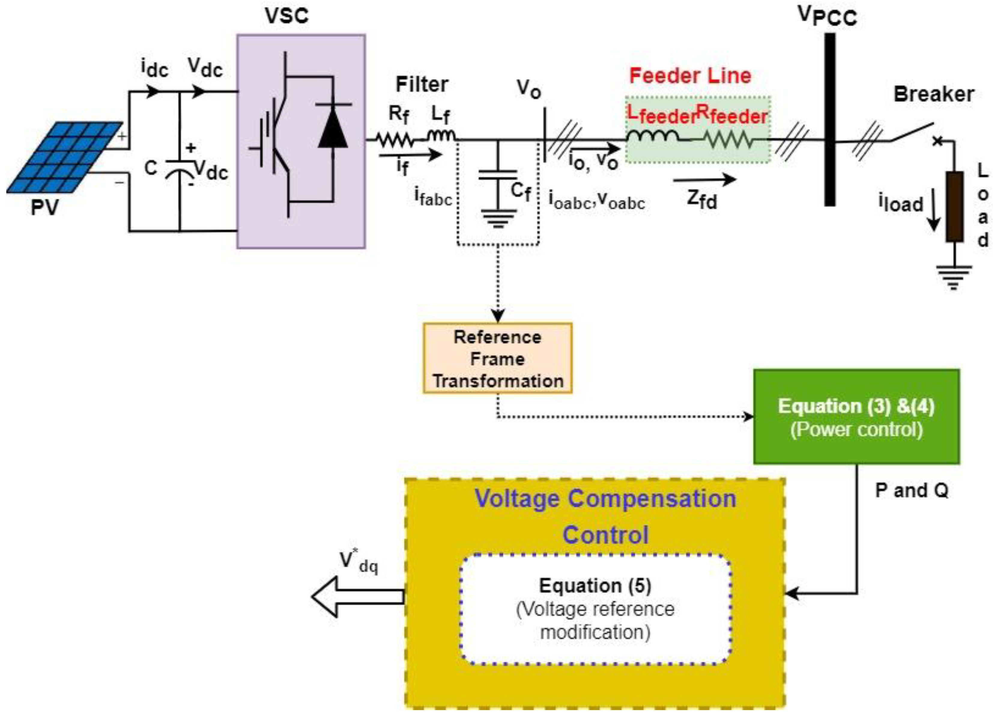
2. Proposed Control Scheme

In this section, the improved control scheme’s development is described. The controller used an adaptive virtual impedance (AVI) loop as the inner-loop control, which responds to the mismatch line impedance. The adaptability of the model predictive control (MPC) used was based on the error input to the cost function as derivative terms of the controller response. In the end, the control model with AVI-FCS MPC was integrated for improvements in the PCC with the standard mathematical model of AVI.

2.1. Power Calculations

The power calculation concept is explained by considering DG inverters with mismatched line impedances, as presented in Figure 1. The P and Q of the ith inverter connected to the PCC are given in Equations (1) and (2), respectively, with X/R considered to be very high and θ = 90° because of the dominance of inductive grid impedance [44]:
P i = 1 X f d ( V o V P C C ( sin δ i ) )
Q i = V o X f d ( V o V P C C ( cos δ i )
From Equations (1) and (2), it is concluded that P is affected by the phase angle, while Q depends on the voltage difference between Vo and VPCC, considering the X/R ratio.

2.2. Reference Voltage Modification for AVI Input

In the islanded mode, frequency and voltage are adjusted by applying the P-V and Q-ω relationships for power characteristics the same as droop concept. Considering the reference voltages, are equal to zero for the islanded mode, as stated in [45,46]:
V = V n o m m p P i
ω = ω n o m + n q Q i
where mp and nq are coefficients and Vnom and ωnom are nominal voltage and frequency, respectively. In conventional control, DGs do not share accurate power due to voltage deviations at the PCC when the line impedances of the connected feeders are not the same.
As mentioned, for resistive-inductive or medium transmission lines, voltage drops at the PCC must be compensated for parallel-connected DGs with mismatched feeder impedances. For power control, the reference voltages described above are altered in the dq frame with PI mechanism in order to minimize the error between the voltage and frequency at the PCC, which can be presented as follows:
[ V d * V q * ] = [ ( k p v ( V n o m V o d ) + k i v 0 t ( V n o m V o d ) d τ ) ( k p v ( V n o m V o q ) + k i v 0 t ( V n o m V o q ) d τ ) ] . [ V n o m d m p P i V n o m q m p P i ]
where kpv and kiv are the PI controller’s gains, V* is the reference voltage when considering fundamental power equations, Vo is the output voltage, and Vnom is the nominal voltage. Figure 2 shows the block diagram of voltage compensation control, along with the calculation for voltage generation to be the input voltage parameter to the AVI.

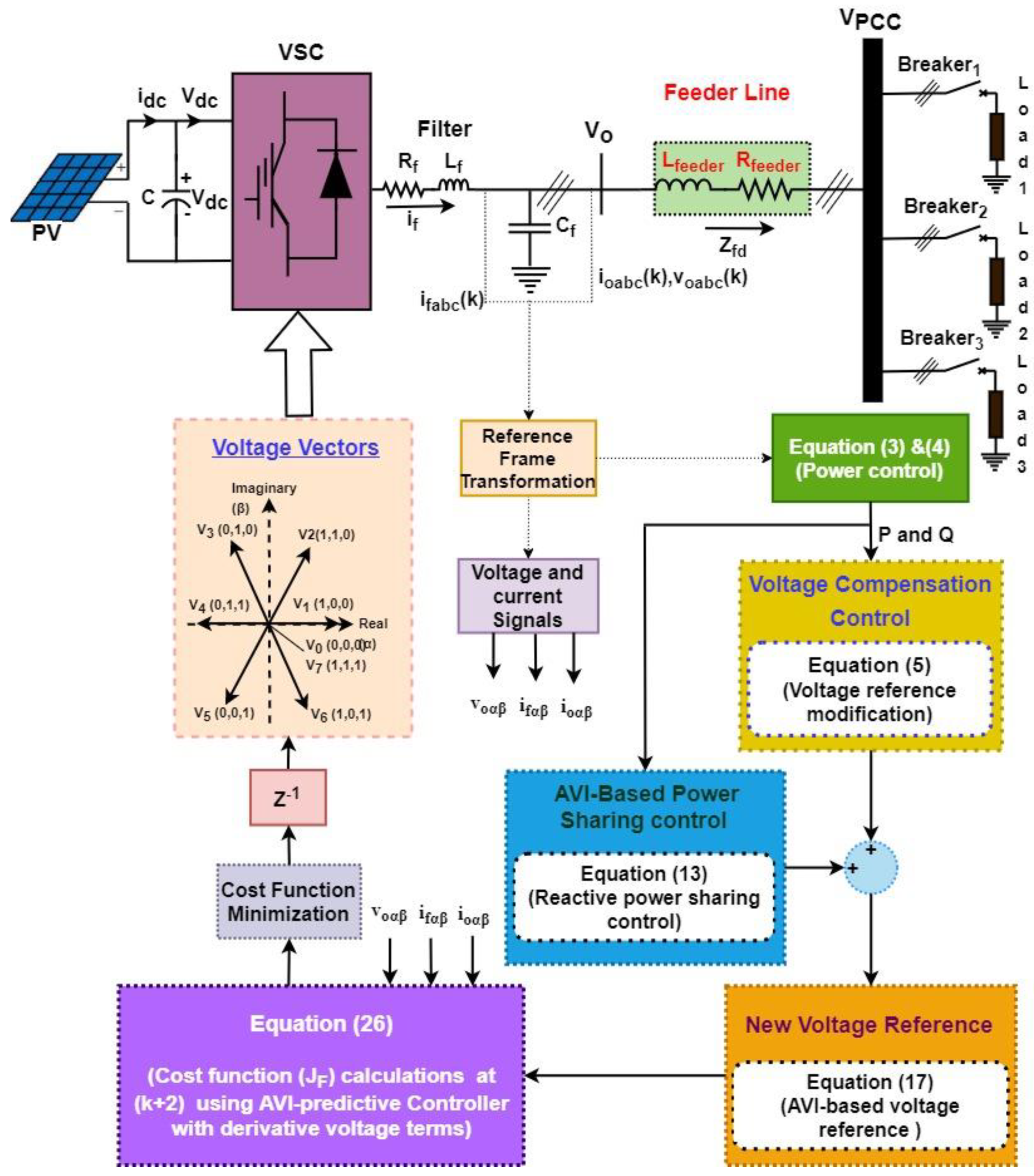
2.3. Adaptive Virtual Impedance (AVI) Model

In order to compensate for voltage drops due to mismatched line impedances, an adaptive virtual impedance loop was added in voltage control to create a new reference voltage. The voltage from droop control for a single inverter is modified as follows:
[ V A V I d V A V I q ] = [ R v i r ω n o m L v i r ω n o m L v i r R v i r ] [ i o d i o q ]
where Rvir, ωnom, and Lvir are the resistive virtual impedance, nominal frequency ( ω = 2 π f n o m ), and inductive virtual impedance, respectively, while iod and ioq are output currents in the dq reference frame. The addition of the adaptive virtual impedance is represented as follows:
[ V A V I q * V A V I q * ] = [ V d * V q * ] + [ V A V I d V A V I q ]
[ V A V I d * V A V I q * ] = [ [ ( k p v . ( V n o m V o d ) + k i v 0 t ( V n o m V o d ) d τ ) k p v . ( V n o m V o q ) + k i v 0 t ( V n o m V o q ) d τ ) ] . [ V n o m d m p P i V n o m q m p P i ] ] + [ R v i r ω n o m L v i r ω n o m L v i r R v i r ] [ i o d i o q ]
With the addition of the adaptive virtual impedance (right end of Equation (8)), the total line impedance is obtained from the virtual and physical impedances of the feeder line, and so the reference voltages can be expressed as follows:
[ V A V I d * V A V I q * ] = [ [ ( k p v . ( V n o m V o d ) + k i v 0 t ( V n o m V o d ) d τ ) k p v . ( V n o m V o q ) + k i v 0 t ( V n o m V o q ) d τ ) ] . [ V n o m d m p P i V n o m q m p P i ] ] + [ ( R v i r + R f e e d e r ) ( ω n o m ( L v i r + L f e e d e r ) ) ( ω n o m ( L v i r + L f e e d e r ) ) ( R v i r + R f e e d e r ) ] [ i o d i o q ]
where Rvir and Lvir are resistive and inductive virtual impedances, respectively, while VAVI is the new reference voltage from the adaptive virtual impedance, Vod/oq is the output voltage, Vnom is the nominal voltage, io is the output current of the converter, and [ R v i r ω n o m L v i r ω n o m L v i r R v i r ] is the virtual impedance loop. As the islanded system considered in this study consisted of two inverters connected in parallel, labelled as DG1 and DG2, the above equations are therefore restated as 1 for the first inverter and 2 for the second inverter in the parallel inverters network:
[ V A V I d 1 * V A V I q 1 * ] = [ [ ( k p v 1 . ( V n o m V o d 1 ) + k i v 1 0 t ( V n o m V o d 1 ) d τ ) k p v 1 . ( V n o m V o q 1 ) + k i v 1 0 t ( V n o m V o q 1 ) d τ ) ] . [ V d 1 V q 1 ] ] + [ ( R v i r 1 + R f e e d e r 1 ) ( ω n o m ( L v i r 1 + L f e e d e r 1 ) ) ( ω n o m ( L v i r 1 + L f e e d e r 1 ) ) ( R v i r 1 + R f e e d e r 1 ) ] [ i o d 1 i o q 1 ]
[ V A V I d 2 * V A V I q 2 * ] = [ [ ( k p v 2 . ( V n o m V o d 2 ) + k i v 2 0 t ( V n o m V o d 2 ) d τ ) k p v 2 . ( V n o m V o q 2 ) + k i v 2 0 t ( V n o m V o q 2 ) d τ ) ] . [ V d 2 V q 2 ] ] + [ ( R v i r 2 + R f e e d e r 2 ) ( ω n o m ( L v i r 2 + L f e e d e r 2 ) ) ( ω n o m ( L v i r 2 + L f e e d e r 2 ) ( R v i r 2 + R f e e d e r 2 ) ] [ i o d 2 i o q 2 ]
The P-Q sharing from the voltage control is modified to compensate for voltage drops, and power-sharing accuracy considering the AVI loop is taken as (single inverter):
[ V A V I d * V A V I q * ] = [ [ ( k p v . ( V n o m V o d ) + k i v 0 t ( V n o m V o d ) d τ ) k p v . ( V n o m V o q ) + k i v 0 t ( V n o m V o q ) d τ ) ] . [ ( V n o m m p P i ) ] ] + [ R v i r ω n o m L v i r ω n o m L v i r R v i r ] [ i o d i o q ]
where the reference voltage from the conventional power control is defined as V = V n o m m p P i at [47]. However, Q is dependent on the impedances of the parallel-connected inverters. The inductive component of the AVI is obtained from the PI control model, which compensates for the error between the total reactive power (Qt) and the reactive power (Q) of an individual DG inverter, expressed as follows:
L v = k p L . ( Q t Q ) + k i L 0 t ( Q t Q )   d τ
From Equation (13), the reference voltages in the dq reference frame can be computed as follows:
[ V r e f d * V r e f q * ] = [ R v i r + ω n o m L v i r ω n o m L v i r R v i r ] [ i o d i o q ]
From Equations (13) and (14), the P-Q sharing accuracy in the dq reference frame for the DG-inverter-based system with mismatched feeder impedances is calculated as follows:
[ V r e f d * V r e f q * ] = [ [ ( k p v . ( V n o m V o d ) + k i v 0 t ( V n o m V o d ) d τ ) k p v . ( V n o m V o q ) + k i v 0 t ( V n o m V o q ) d τ ) ] . [ ( V n o m m p P i ) ] ] + [ [ k p L . ( Q t Q ) + k i L 0 t ( Q t Q )   d τ ] [ R v i r + ω n o m L v i r ω n o m L v i r R v i r ] [ i o d i o q ] ]
Finally, with Rvir and Lvir added to the system, Equation (15) can be represented as in Equation (16):
[ V r e f d * V r e f q * ] = [ [ ( k p v . ( V n o m V o d ) + k i v 0 t ( V n o m V o d ) d τ ) k p v . ( V n o m V o q ) + k i v 0 t ( V n o m V o q ) d τ ) ] . [ ( V n o m m p P i ) ] ] + [ [ k p L . ( Q t Q ) + k i L 0 t ( Q t Q )   d τ ] [ ( R v i r + R f e e d e r ) ω n o m ( L v i r + L f e e d e r ) ω n o m ( L v i r + L f e e d e r ) ( R v i r + R f e e d e r ) ] [ i o d i o q ] ]
The implementation of the proposed AVI aimed to adaptively change the impedance inductor at Lvir according to the system’s behavior with the addition of loads. The control strategy used in this study used the decentralized mode and was applied to both parallel-connected DG1 and DG2 inverters with mismatched line impedances.
For DG1 and DG2, Equation (15) can be separately expressed as in Equation (17):
[ V r e f d 1 , 2 * V r e f q 1 , 2 * ] = [ [ ( k p v 1 , 2 . ( V n o m V o d 1 , 2 ) + k i v 1 , 2 0 t ( V n o m V o d 1 , 2 ) d τ ) k p v 1 , 2 . ( V n o m V o q 1 , 2 ) + k i v 1 , 2 0 t ( V n o m V o q 1 , 2 ) d τ ) ] . [ ( V n o m m p 1 , 2 P 1 , 2 ) ] ] + [ [ k p L 1 , 2 . ( Q t Q 1 , 2 ) + k i L 1 , 2 0 t ( Q t Q 1 , 2 )   d τ ] [ ( R v i r 1 + R f e e d e r 1 ) ω n o m ( L v i r 1 + L f e e d e r 1 , 2 ) ω n o m ( L v i r 1 + L f e e d e r 1 ) ( R v i r 1 , 2 + + R f e e d e r 1 , 2 ) ] [ i o d 1 , 2 i o q 1 , 2 ] ]
The alpha-beta (αβ) components can be obtained by taking the inverse Park transformation of Equation (17):
V r e f α β 1 * = V 1 r e f α * j V r e f β 1 * = [ 1 j ] . [ cos θ sin θ sin θ cos θ ] . [ V r e f d 1 * V r e f q 1 * ]
V r e f α β 2 * = V r e f α 2 * j V r e f β 2 * = [ 1 j ] . [ cos θ sin θ sin θ cos θ ] . [ V r e f d 2 * V r e f q 2 * ]
Reference voltages V r e f α β 1 * and V r e f α β 2 * are applied to the next FCS-MPC controller’s inputs to accurately track the output voltage for power-sharing accuracy and voltage compensation at the PCC, which is discussed in the next section.

2.4. Inverter LC Filter

The inverter model was based on a VSC with an LC filter, where dynamic behaviors of voltage and current were obtained by considering the inductor current and capacitor as the inverter plant. The continuous-time state-space model was converted into the discrete-time model utilizing the zero-order hold (ZOH) [48].
The d d t [ v o α β i f α β ] for the LC filter is given as follows:
d d t [ v o α β i f α β ] = A . [ v f α β i f α β ] + B . [ v i α β i o α β ]
where A and B are as follows:
A = [ R f L f 1 L f 1 C f 0 ]
B = [ 1 L f 0 0 1 C f ]
The discrete model obtained from the ZOH for the discrete LC filter can be formulated as follows:
[ i f α β v o α β ] = A d [ i f α β v o α β ] + B d [ v i α β i o α β ]
where A d = e A T s a n d   B d = 0 T s e A τ . B d τ . The values for viαβ are measured from the switching states. Based on the discrete model presented in Equation (20), output current io is measured for vi (input vector for each possible switching state). The output voltage and current are also measured for every possible value of viαβ. The optimized values of the switching inputs at a particular time instance are used for cost function (CF) minimization at the MPC controller where the same mechanism is repeated for the next sampling time. The FCS-MPC development was based on a two-step receding horizon for the measurement of voltage and current to reduce computational errors and compensate for delay time. Therefore, the discrete state-space system can be defined as follows:
[ i f α β ( k + 1 ) v o α β ( k + 1 ) ] = A d [ i f α β ( k ) v o α β ( k ) ] + B d [ v i α β ( k ) i o α β ( k ) ]
where k + 1 and k are time instances, represented as (k + 1). Ts and (k). Ts, respectively, where Ts represents the sampling time period.

2.5. VSC Vector Switching with AVI FCS MPC Controller

The inverter used in this project had three gate signals, which were Sa, Sb, and Sc. The two switches for each leg offer two possible setting states, which are 0 and 1 [49], with the inverter voltage obtained as follows:
v i a b c = [ v i a v i b v i c ] = [ v i a v i b v i c ] [ v i a N + v i b N + v i c N 3 ]
Equation (22) can be represented by matrix calculation as follows:
v i a b c = [ v i a v i b v i c ] = [ V d c . ( I 1 3 1 ) . S ]
where I is the identity matrix, 1 is an all-ones 3 × 3 matrix, and S is the switching action of the inverter:
I = [ 1 0 0 0 1 0 0 0 1 ] ,   1 = [ 1 1 1 1 1 1 1 1 1 ] ,   S = [ S a S b S c ]
Therefore, Equation (23) shows that eight possible switching states can be generated for different configurations. A maximum of eight input voltage vectors are obtained from the switching state arrangements.

3. CF Based on Adaptive Virtual Impedance

The CF considered the derivative terms of capacitor voltage, which was modified for the case of feeder impedance mismatch, where the reference voltage created by using the AVI was substituted to track the reference output voltage (415 V at target PCC), i.e., d d t ( v o ( t ) ) would track d d t ( v r e f ( t ) ) , which included the derivative terms. The CF based on derivative terms for the AVI-based controller with the voltage compensation loop and receding-horizon two-steps-ahead predictions is written as follows:
J A V I = ( C f . ω r e f . v r e f α ( k + 2 ) ) i f α ( k + 2 ) + i o α ( k + 2 ) ) 2 + ( C f . ω r e f . v r e f β ( k + 2 ) ) i f β ( k + 2 ) + i o β ( k + 2 ) ) 2
The CFs for DG1 and DG2 from Equation (24) use decentralized controllers and can be expressed as follows:
J A V I 1 , 2 = ( C f 1 , 2 . ω r e f 1 , 2 . v r e f α 1 , 2 ( k + 2 ) ) i f α 1 , 2 ( k + 2 ) + i o α 1 , 2 ( k + 2 ) ) 2 + ( C f 1 , 2 . ω r e f 1 , 2 . v r e f β 1 , 2 ( k + 2 ) ) i f β 1 , 2 ( k + 2 ) + i o β 1 , 2 ( k + 2 ) ) 2
In this study, the reference voltage, V r e f * , was generated to mitigate feeder impedance mismatch, which is based on power control modification, and the voltage compensation loop with the addition of the AVI was designed to track and compensate for voltage deviations at the PCC as given in AVI Section 2.3. Moreover, reactive power-sharing errors due to mismatched line impedances were covered by the AVI-based control as the inner-loop configuration. The complete CF, which can track the reference voltage and its derivative for DG1 and DG2, is given as follows:
J F 1 , 2 = [ ( V r e f α 1 , 2 [ k + 2 ] v o α 1 , 2 [ k + 2 ] ) + ( V r e f β 1 , 2 [ k + 2 ] v o β 1 , 2 [ k + 2 ] ) 2 ] + λ d ( ( C f 1 , 2 . ω r e f 1 . v r e f α 1 , 2 ( k + 2 ) ) i f α 1 , 2 ( k + 2 ) + i o α 1 , 2 ( k + 2 ) ) 2 + ( C f 1 , 2 . ω r e f 1 , 2 . v r e f β 1 , 2 ( k + 2 ) ) i f β 1 , 2 ( k + 2 ) + i o β 1 , 2 ( k + 2 ) ) 2 ) + h lim + λ u s w 2
where λ u   a n d   λ d are weighting factors to address uncertainties, h lim ( i ) = 0 when i f ( i ) i max , h lim ( i ) = when i f ( i ) > i max , s w ( i ) = ( u ( i ) u ( i 1 ) ) , and [ ( V r e f α [ k + 2 ] v o α [ k + 2 ] ) + ( V r e f β [ k + 2 ] v o β [ k + 2 ] ) 2 ] = J 1   ( C f . ω r e f . v r e f α ( k + 2 ) ) i f α ( k + 2 ) + i o α ( k + 2 ) ) 2 + ( C f . ω r e f . v r e f β ( k + 2 ) ) i f β ( k + 2 ) + i o β ( k + 2 ) ) 2 = J A V I 1 .
The Simulink block diagram of the cost function calculations for the proposed AVI-FCS MPC for a single inverter is shown in Figure 3. The CF with uncertainties was considered to find weighting factors λ u   a n d   λ d in order to tune the controller’s error.

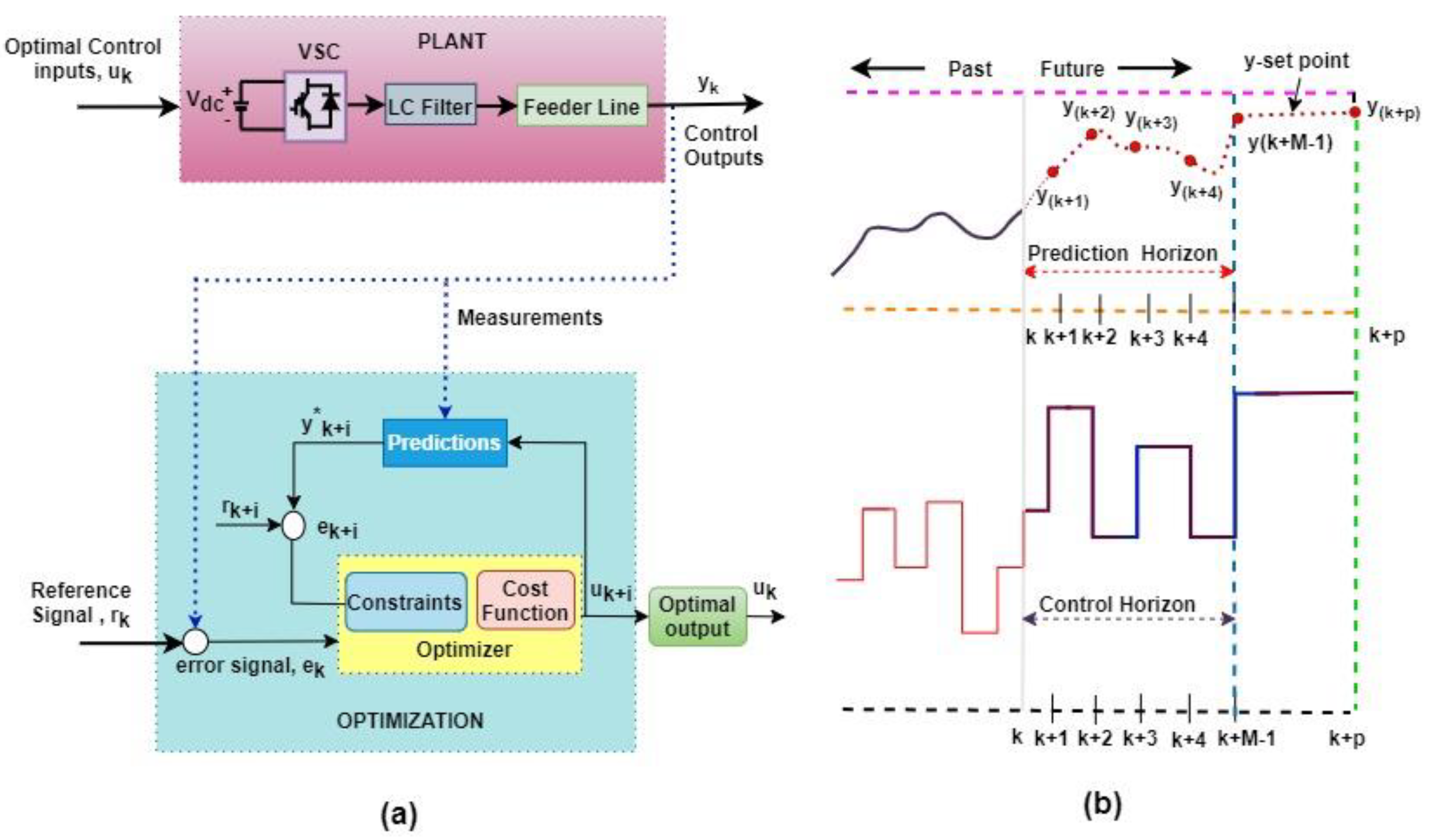
4. CF Optimization and Prediction Algorithms as Space-Vector Improvement

The optimization process in the proposed AVI-CF is shown in Figure 4a,b. The constraints in MPC controller optimization are resolved over the prediction horizon so that the next control action is evaluated. The present state of optimization evaluated by the control law is repeated again in the next time step to update the MPC control law. The significance of the control feature of MPC is a solution to optimization problems. Figure 4b shows the control output (yk) and the manipulated input (uk) with time steps (k + 1), (k + 2), and so on. The control moves are according to the pre-decided time steps moving to the horizon window. The decision for the present control move (Ts) is held until the second time instant, 2 × Ts, in a discrete time interval for the digital controller. With a small Ts, a system is more continuous and can more accurately track the reference signal (rk). For the time instant, control moves are taken as u ( t ) = k T s , and so the output yk changes accordingly with the given sampling time. The error ek between y and the y-setpoint is computed at sampling times k + 1, k + 2, k + 3, and so on.
The error between y and y-setpoint to give the predicted value of yp is intended to be as small as possible by taking into consideration the p-times-ahead prediction, y(k + p), where p is the prediction horizon. So, the change at the u(k) step has an effect on y(k + 1) because the change is made using the same time interval. The maximum value (M) at the control horizon taken by the controller must be less than or equal to the predicted value. After k + p, there is no effect on u (input control), as the setpoint is already attained, and generally, M is taken to be much smaller than p. The notion of prediction horizon has been used to solve optimization problems by considering objectives, constraints, and decision-making variables. The error between y and ysp is calculated and the intention is to obtain an almost zero error. So, the sum of squares of the errors are taken to minimize the cost function. Mathematically, it can be written as follows:
0 = i = 1 p [ y ( k + i ) y s p ] 2
The constraints exist in FCS-MPC controllers’ S-function of decision variables in CF. Generally, for the control input for M variables of u(k), u(k + 1), u(k + 2), …, u(k + M − 1) irrespective of k, the time step for the lower and upper limits can be written as ∆u = u(k) − u(k − 1). The decision variables are taken as given below for the CF prediction value:
u L u u u
u L u u u
0 = i = 1 p [ y ( k + i ) y s p ] 2 + i = 1 M [ u ( k + i 1 ) ] 2

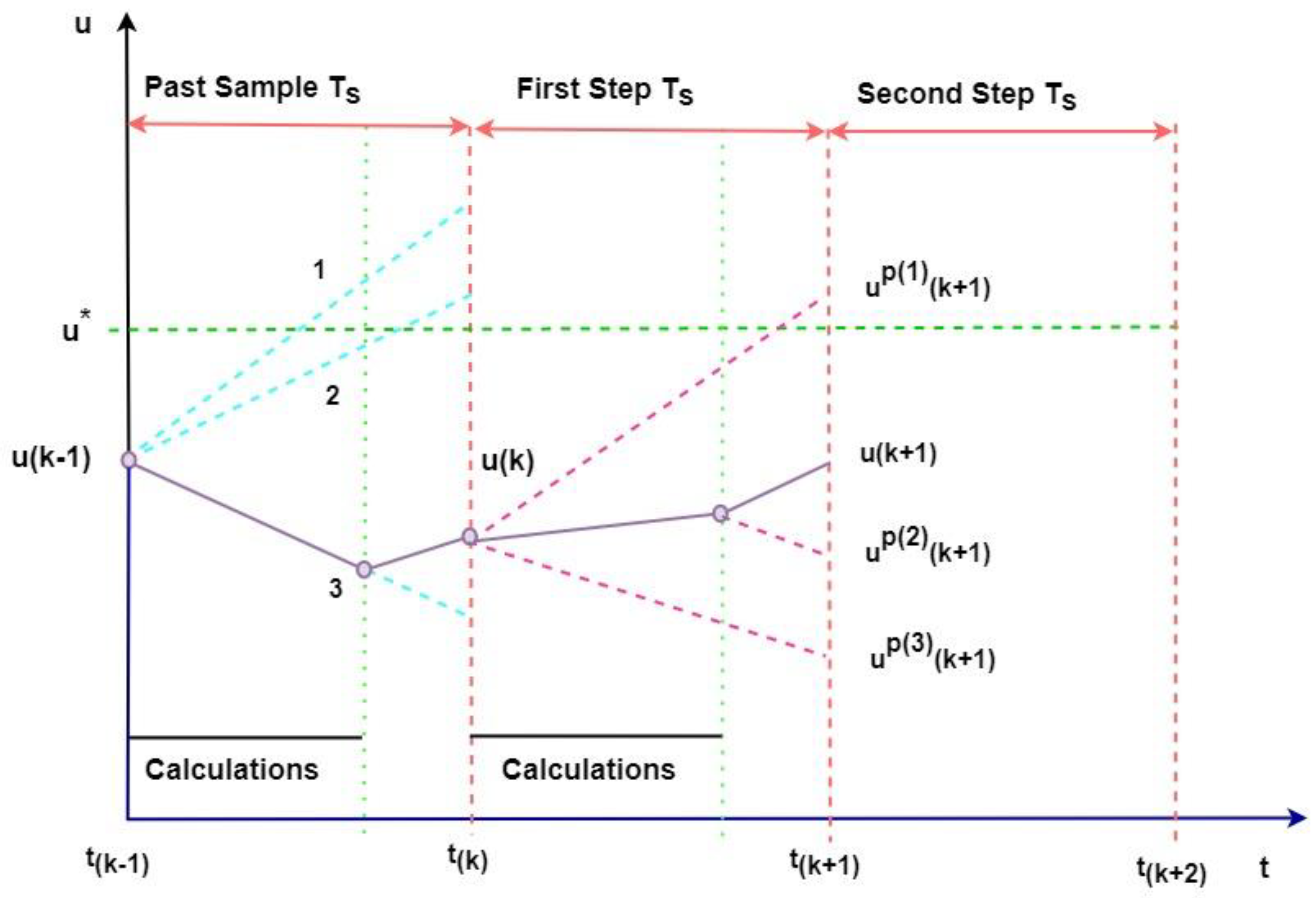
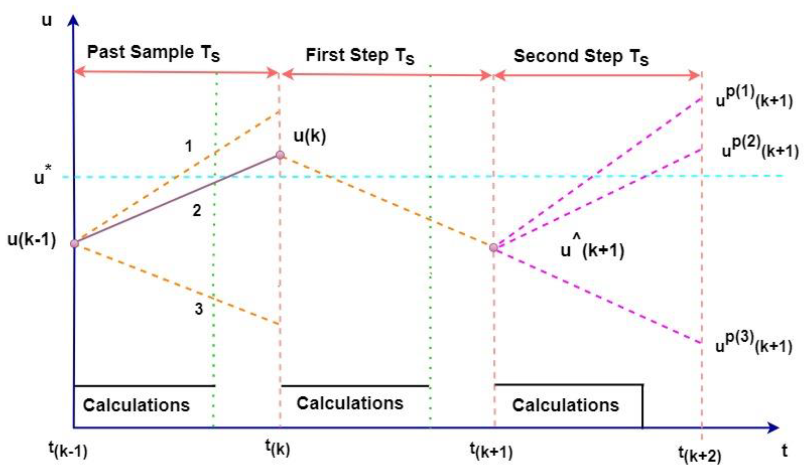
5. Computational Burden Reduction and Time Delay Compensation at MPC Time Step

The FCS-MPC computation burden results in time delay, which reduces reference tracking efficiency. Figure 5 shows the time delay due to the computational burden with control input signal u and its predictions up to kth time at sampling time Ts [50].
In this study, the control algorithms were separated from the optimization algorithms at time delay compensation based on the sampling time. One sampling interval was used for time delay compensation to reduce the computational time delay, whereas another sampling interval was used for the optimization algorithms. So, the CF was computed at two-steps-ahead (k + 2) predictions and the selected optimized output was then applied for the next switching-state sampling interval (k + 1). Therefore, the controller must predict the values at the k + 1 sampling time given the measurements and the control law at the k sampling time and then find the optimal control law to be applied to the next sampling time. In other words, the control law at the k sampling time would produce a response in the system at the k + 1 sampling time, the control law at the k + 1 sampling time would produce a response in the system at the k + 2 sampling time, and so on, as shown in Figure 6.
For time delay compensation, the optimal switching state of the prior iteration, xopt(k), was applied for the estimation of the control variable at the k + 1 interval, at ( u ^ ( k + 1 ) ) . From ( u ^ ( k + 1 ) ) , the control variable was predicted at the k + 2 interval. So, at k + 2, Equation (21) can be represented as follows:
[ i f α β ( k + 2 ) v o α β ( k + 2 ) ] = A d [ i f α β ( k + 1 ) v o α β ( k + 1 ) ] + B d [ v i α β ( k + 1 ) i o α β ( k + 1 ) ]
It is important to note that Equation (31) is a recursive equation, which means that to find the values at k + 2, one must obtain the values at k + 1 first. Thus, the values at k + 2 depend on the values at k + 1, which also depend on the values at k, and so forth. In Equation (31), all the variables can be predicted, except output current ioαβ(k + 1) because it depends on the load connected at the output. Moreover, this variable would be measured and not calculated. However, since the output current has low-frequency components, it is reasonable to assume that there are no major differences between two continuous samples, and therefore i o α β ( k + 1 ) ; i o α β ( k ) . From Equation (31), the input variables and their controlled input, u(k), are expressed as follows:
x ( k ) = [ i f α β ( k ) v o α β ( k ) ] , u ( k ) = [ i o α β ( k ) v i α β ( k ) ]
So, x(k + 2) is formulated as follows:
x [ k + 1 ] = A d . x [ k ] + B d . u [ k ]
x [ k + 2 ] = A d . x [ k + 1 ] + B d . u [ k + 1 ]
x [ k + 2 ] = A d 2 . x [ k ] + A d . B d . u [ k ] + B d . u [ k + 1 ]
The controller input signals using k + 2 prediction to track the reference signals were used to develop the proposed FCS MPC-based predictive control to compensate for voltage drops due the mismatched feeder lines in an islanded microgrid.

6. Circulating Current Error Estimation Measurement

The current that reverse flow into inverters due to mismatched line impedances is known as the circulating current. The circulating current can lead to increased power losses, overloaded inverters, and reduced power quality and efficiency. Decentralized control has more issues related to circulating currents than centralized control. For parallel-connected inverters, the circulating current can be estimated using Equation (36):
i H i = k i i u n i t i o i
where:
i u n i t = i = 1 n i o i i n k i
In the above equation, ioi denotes the output current, iHi denotes the circulating current, and ki denotes the ratio of the nominal capacity of the ith inverter in parallel. For example, the circulating currents for two inverter VSCs connected in parallel can be calculated as follows:
i H 1 = k 1 i o 1 + i o 2 k 1 + k 2 i o 1 = 1 k 1 + k 2 ( k 1 . i o 2 k 2 . i o 1 )
i H 2 = k 1 i o 1 + i o 2 k 1 + k 2 i o 2 = 1 k 1 + k 2 ( k 2 . i o 1 k 1 . i o 2 )
where k1 and k2 are the capacities of the parallel-connected inverters. In this study, both parallel-connected DGs had a capacity of 1.5 kW. Therefore, k1 was equal to k2 in this case. The relationships in Equations (37) and (38) were used to circulate current measurements and were modeled in Simulink for this research work.
Table 1 shows the parameter values for the two inverters connected in parallel at the same PCC with different line impedances. The model was connected with a load (1200 W, 550 Var) at the PCC to create a power-sharing condition for the system.

7. Results: Discussion and Comparison

The system with an RL load connected at the PCC was investigated under the condition of mismatched line impedances for both inverters. The results were compared with those of static virtual impedance (SVI)-based and conventional (PI) control techniques. Table 1 shows the parameter values. The design processes of the PI and SVI controllers are not discussed in this paper.

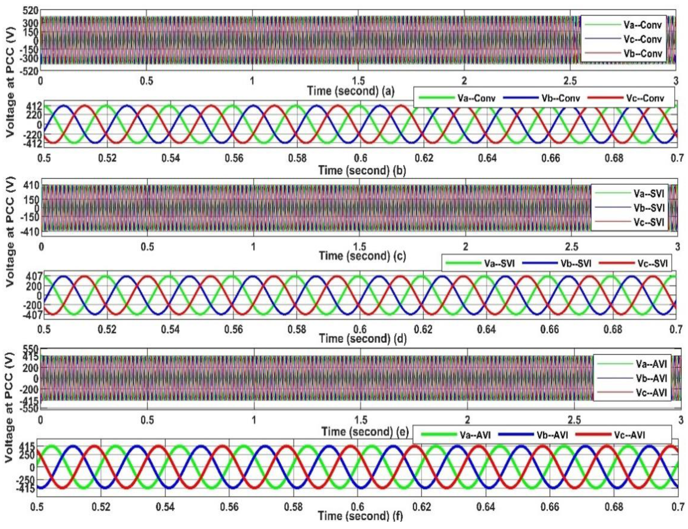
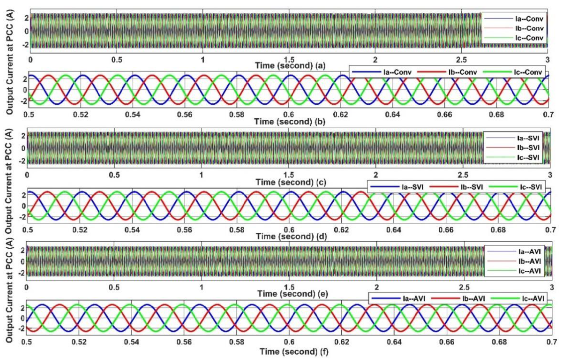
7.1. Comparison of Voltage and Current at PCC between Conventional, SVI-Based, and AVI-Based Controllers

The result of the voltage at the PCC for the conventional control scheme is shown in Figure 7a, with the zoomed-in image shown in Figure 7b. The voltage at the PCC for the SVI-based controller is shown in Figure 7c and the zoomed-in version is shown in Figure 7d. The target voltage or reference voltage at the PCC was set at 415 V. For the PI controller, the voltage at the PCC was about 412 V instead of 415 V. The SVI-based controller also gave a low voltage magnitude at the PCC, which was 407 V. The PCC voltage for the proposed AVI-FCS MPC control scheme is shown in Figure 7e, and the zoomed-in image at the time interval of 0.5–0.7 s is shown in Figure 7f. Its voltage magnitude was maintained at 414.95 V. Therefore, it is clear that the proposed control scheme maintained the voltage magnitude at the PCC in the case of parallel-connected inverters with mismatched line impedances.
The output current at the PCC for the PI control scheme is shown in Figure 8a, with the zoomed-in image shown in Figure 8b. Its current was maintained at 2.53 A throughout the simulation period for the conventional control scheme. As for the SVI-based control scheme and the proposed AVI-FCS MPC control scheme, their output current values were 2.5 A and 2.4 A, respectively, as shown in Figure 8c–f.

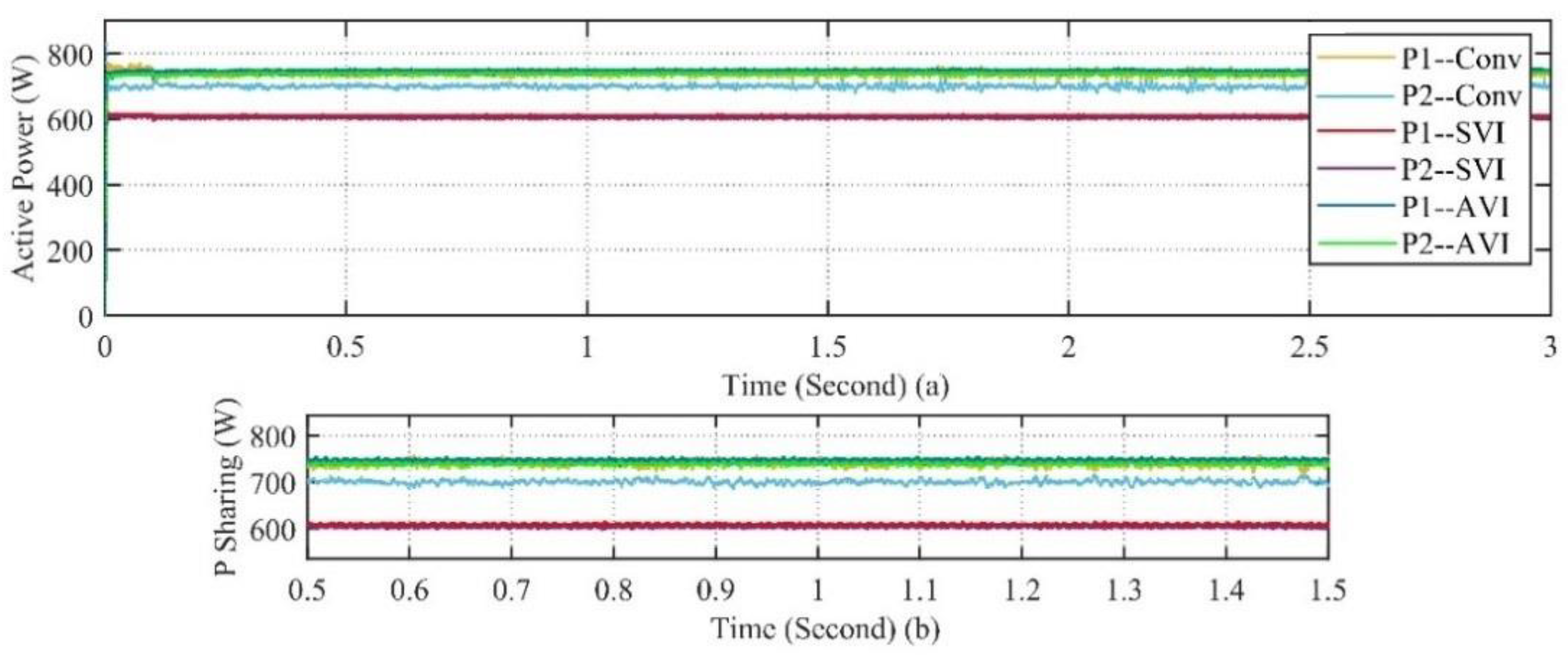
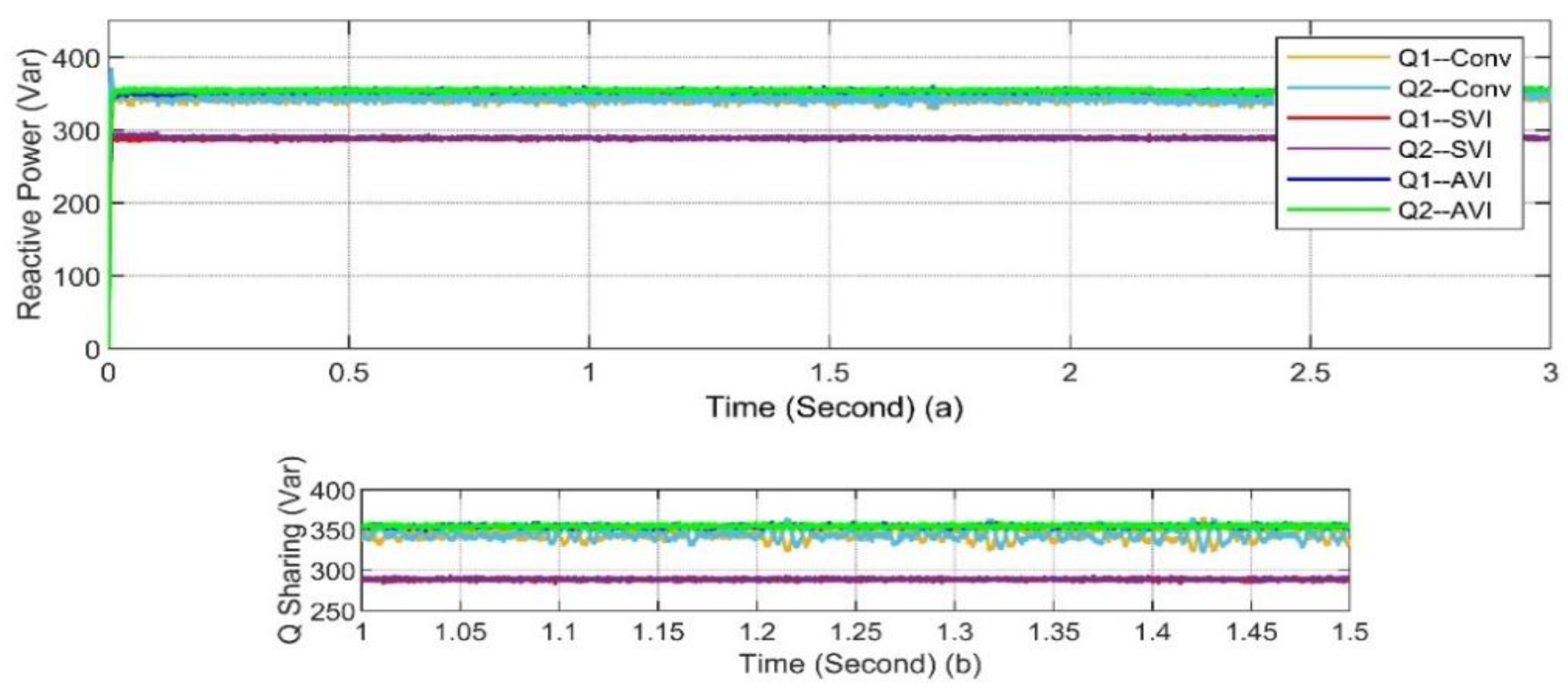
7.2. PCC Active and Reactive Power-Sharing Comparison

Next, the comparison of active power sharing between both DG inverters for the PI control, SVI-based control, and proposed control schemes is shown in Figure 9a. The zoomed-in image is given in Figure 9b. Under the PI control scheme, the active power shared by DG1 was 750 W and the active power shared by DG2 was 700 W per the connected load. When SVI-based control was applied, DG1 and DG2 both shared 610 W equally. Under the proposed control scheme, the value at the PCC of the active power shared by each inverter connected in parallel was 749.9 W per the load. So, it can be seen that both DG inverters shared accurate and equal active power per the connected load under the proposed AVI-FCS MPC control scheme. Under the PI and SVI-based control schemes, DG1 and DG2 did not share equal and accurate active power as per the connected load.
The comparison of the reactive power shared by DG1 and DG2 is shown in Figure 10. Figure 10a shows the reactive powers measured from 0–3 s, and Figure 10b shows the zoomed-in image of the reactive powers from 1–1.5 s. It can be seen in Figure 10b that the reactive power shared by DG1 and DG2 was 340 Var under the PI control scheme. When the system operated under the SVI-based control scheme, the reactive power shared by the DG inverters was 288 Var. When the system operated under the proposed AVI-based predictive control, the reactive power shared by each DG inverter was 349.8 Var per load. It is clearly shown that the accuracy of reactive power sharing improved under the proposed AVI-based predictive control scheme.

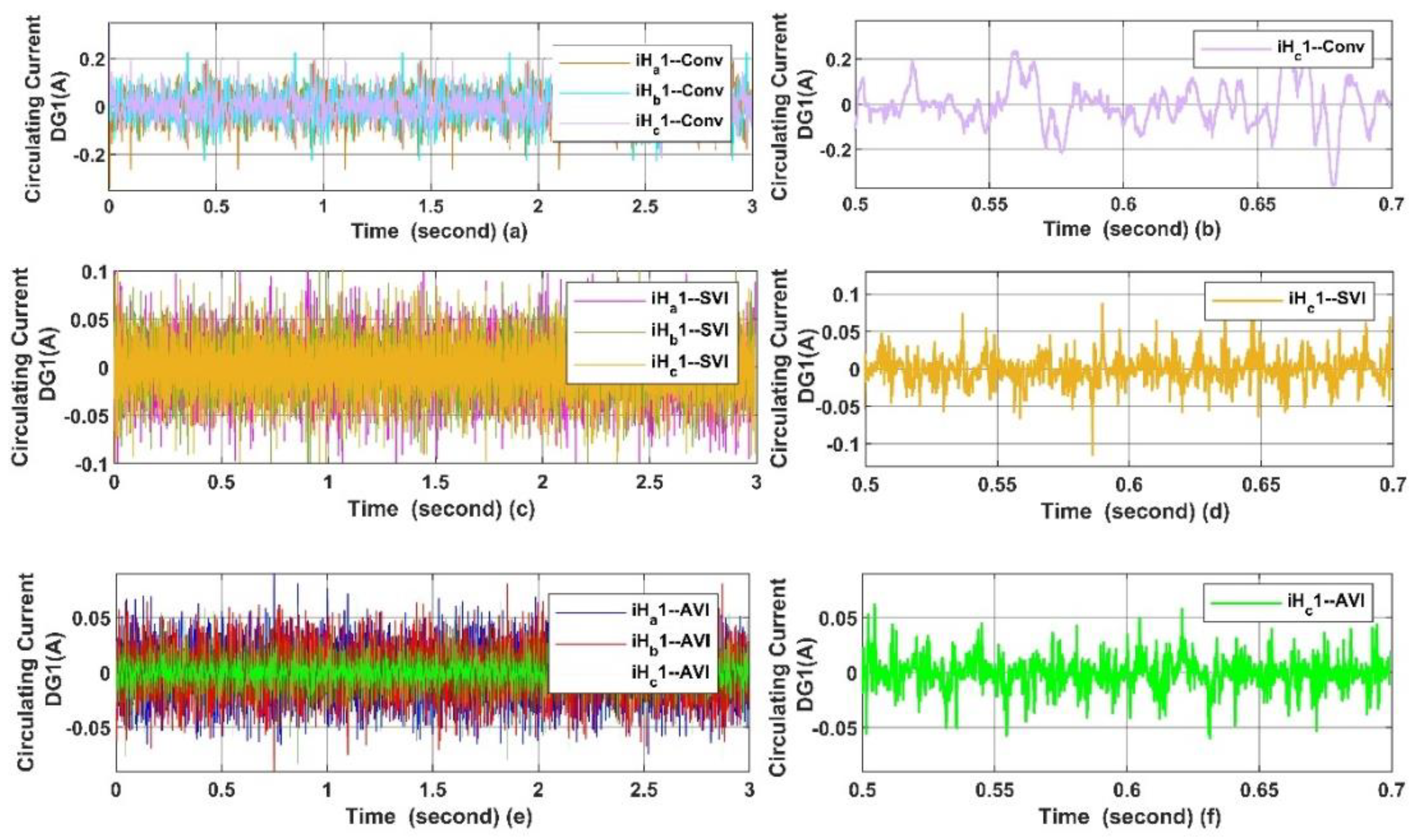
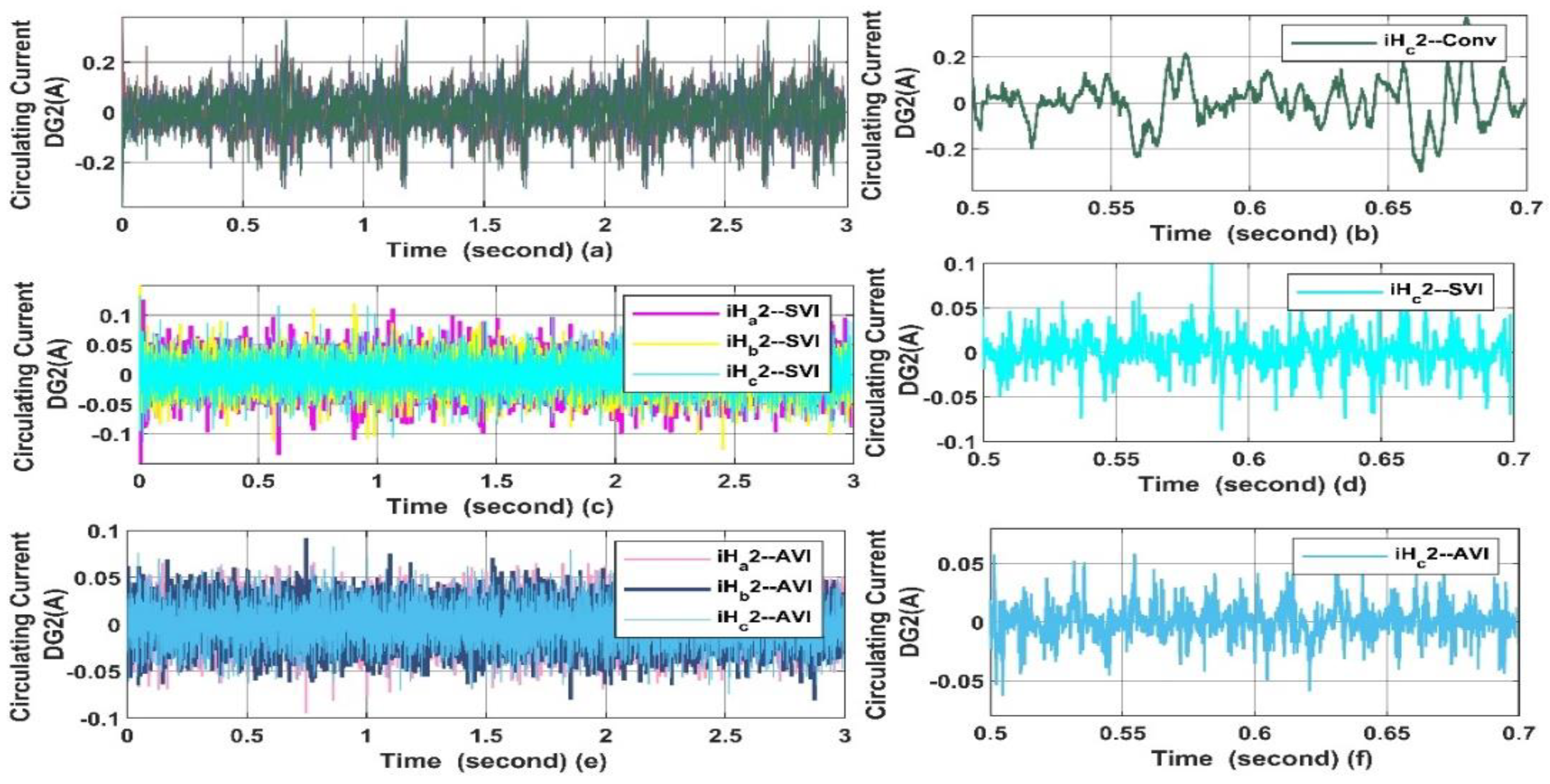
7.3. Circulating Current at PCC

The circulating currents for DG1 and DG2 at the PCC are shown in Figure 11 and Figure 12, respectively. The circulating currents measurements at (iHa1, iHb1, and iHc1) for DG1 under the conventional control scheme are shown in Figure 11a. For clear visualization, the zoomed-in image of the circulating current from 0.5–0.7 s under the PI control scheme is shown in Figure 11b. The circulating current for DG1 was around 0.28 A under the conventional control scheme. Under the SVI-based control scheme, the circulating current for DG1 was 0.065 A, as shown in Figure 11c,d. In contrast, the circulating current for DG1 under the proposed AVI-based predictive control scheme was approximately 0.045 A, as shown in Figure 11e,f.
Figure 12a shows the circulating current for DG2 under the conventional control scheme. The zoomed-in image in Figure 12b illustrates the circulating current for DG2 when the PI control was applied to the system. Its circulating current was almost 0.23 A. As shown in Figure 12c,d, the circulating current for DG2 under the SVI-based control scheme was at 0.066 A. Under the configuration of the proposed AVI-based predictive control scheme, the circulating current was 0.047 A, as shown in Figure 12e,f.

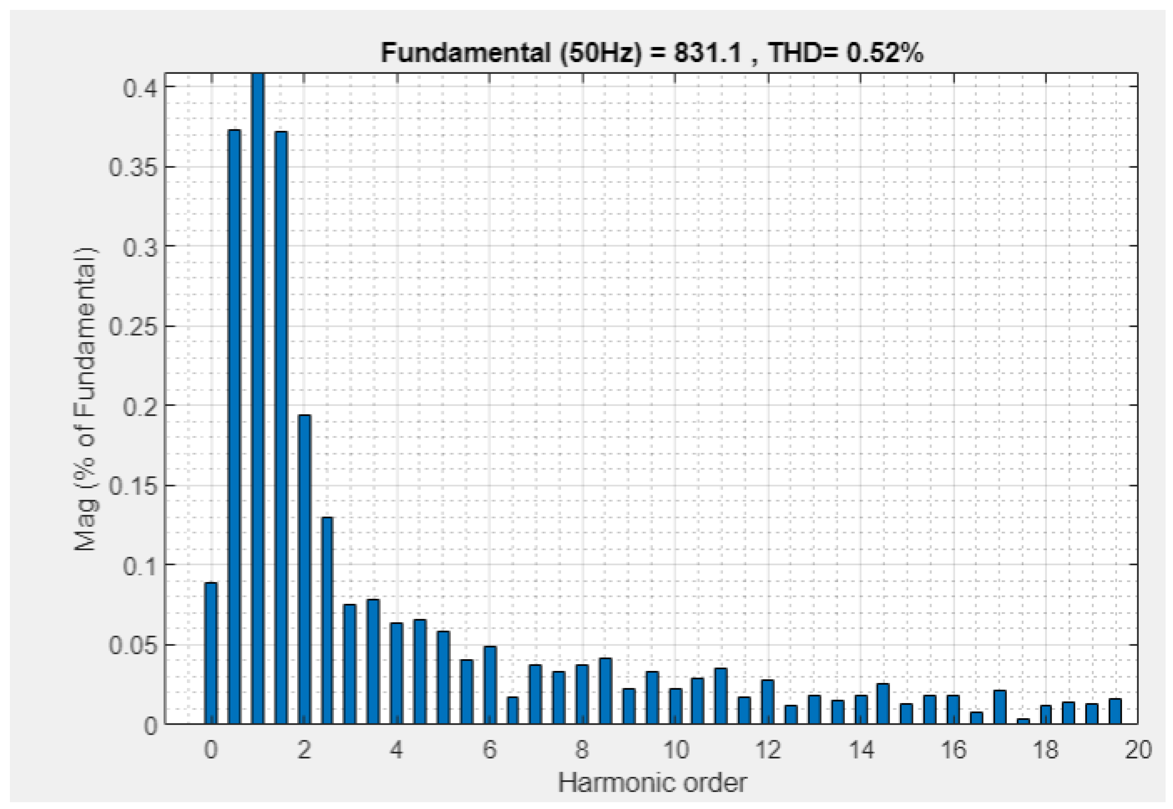
7.4. FFT Spectra Analysis

The FFT spectrum analysis of the proposed AVI-FCS MPC control’s output voltage is given in this subsection. Harmonics are generally caused by switching devices and non-linearity in the connected loads, transformers, and generators used in a system. The analysis was performed to investigate if the total harmonic distortion (THD) at the PCC under the proposed controller scheme was below 5% per the IEEE 519-1992 electrical standard for harmonics [51].
Figure 13 shows the output voltage’s FFT window for Phase A for two cycles when the system was using the proposed control with a load connected at the PCC (common to all parallel inverters). The THD spectrum of the output voltage at the PCC showed that in the THD, the load was connected at the PCC, where the THD was 0.52% at 50 Hz of frequency.
The THD value with the connected load showed that the proposed control scheme had low THD suppression if mismatched line impedances were applied to each inverter.

8. Conclusions

As a conclusion, an AVI FCS-MPC with a decentralized configuration for mismatched line impedances was developed. The proposed control scheme compensated the voltage at the PCC and power-sharing accuracy was maintained at both inverters. The active and reactive power-sharing issues and the circulating current generation caused by the mismatched line impedances of parallel-connected inverters were successfully resolved. With the addition of the adaptive virtual impedance to the physical feeders’ impedances, a new reference voltage was generated. The AVI-based reference voltage generated using the predictive control scheme was used as the input for the FCS-MPC model, which effectively compensated for voltage drops and suppressed the circulating current under the condition of mismatched line impedances. Here, it shows that by having a minimum circulating current, the improved controller can have accurate power sharing and voltage compensation at the PCC, same as when the normal the droop control been applied at short transmission line.

Author Contributions

Conceptualization, M.H.K. and S.A.Z.; methodology M.H.K. and S.A.Z.; investigation, N.T., I.E. and A.B.; writing—original draft preparation, M.H.K. and S.A.Z.; writing—review and editing, N.T., I.E. and A.B.; supervision, S.A.Z. All authors have read and agreed to the published version of the manuscript.

Funding

This research was funded by the Research Management Centre and the Research University Grant Program of Universiti Tun Hussein Onn Malaysia (UTHM) through Tier 1 (vot Q365), and Istanbul Ticaret University, Türkiye.

Data Availability Statement

The data are available from the corresponding author upon reasonable request. The data are not publicly available due to the fact that there are still graduate students using them for research.

Acknowledgments

The authors would like to express their gratitude to everyone who contributed to this research work. In addition, the authors would like to thank the group members of Advanced Control on Power Converters (ACPC) especially Momoh Kabir from, Faculty of Electrical and Electronic Engineering, UTHM, for assisting in the administration of this research.

Conflicts of Interest

The authors of this research paper declare that they have no conflicts of interest to disclose.

References

  1. Hou, S.; Chen, J.; Chen, G. Distributed control strategy for voltage and frequency restoration and accurate reactive power-sharing for islanded microgrid. Energy Rep. 2023, 9, 742–751. [Google Scholar] [CrossRef]
  2. Jasim, A.M.; Jasim, B.H.; Bureš, V.; Mikulecký, P. A New Decentralized Robust Secondary Control for Smart Islanded Microgrids. Sensors 2022, 22, 8709. [Google Scholar] [CrossRef]
  3. Feng, K.; Liu, C. Distributed Hierarchical Control for Fast Frequency Restoration in VSG-Controlled Islanded Microgrids. IEEE Open J. Ind. Electron. Soc. 2022, 3, 496–506. [Google Scholar] [CrossRef]
  4. Hennane, Y.; Pierfederici, S.; Berdai, A.; Meibody-Tabar, F.; Martin, J.P. Distributed control of islanded meshed microgrids. IEEE Access 2023, 11, 78262–78272. [Google Scholar] [CrossRef]
  5. Wang, G.; Duan, G.; Duan, J.; Cao, S.; Song, Y.; Kang, J. An integrated control method of multi-source islanded microgrids. Energy Rep. 2023, 9, 630–636. [Google Scholar] [CrossRef]
  6. Zuo, K.; Wu, L. A review of decentralized and distributed control approaches for islanded microgrids: Novel designs, current trends, and emerging challenges. Electr. J. 2022, 35, 5. [Google Scholar] [CrossRef]
  7. Almousawi, A.Q.; Aldair, P.D.A.A. Design an Accurate Power Control Strategy of Parallel Connected Inverters in Islanded Microgrids. IOP Conf. Ser. Mater. Sci. Eng. 2021, 1105, 012021. [Google Scholar] [CrossRef]
  8. Mai, R.; Lu, L.; Li, Y.; Lin, T.; He, Z. Circulating Current Reduction Strategy for Parallel-Connected Inverters Based IPT Systems. Energies 2017, 10, 261. [Google Scholar] [CrossRef]
  9. Guerrero, J.M.; De Vicuña, L.G.; Matas, J.; Miret, J.; Castilla, M. Output impedance design of parallel-connected UPS inverters. IEEE Int. Symp. Ind. Electron. 2004, 2, 1123–1128. [Google Scholar]
  10. Jin, L.; He, Z. A New Virtual Impedance Method for Parallel. In Proceedings of the 2016 IEEE Vehicle Power and Propulsion Conference (VPPC), Hangzhou, China, 17–26 October 2016; pp. 1–4. [Google Scholar]
  11. Zhang, M.; Song, B.; Wang, J. Circulating current control strategy based on equivalent feeder for parallel inverters in Islanded microgrid. IEEE Trans. Power Syst. 2018, 34, 595–605. [Google Scholar] [CrossRef]
  12. Matas, J.; Castilla, M.; De Vicuña, L.G.; Miret, J.; Vasquez, J.C. Virtual impedance loop for droop-controlled single-phase parallel inverters using a second-order general-integrator scheme. IEEE Trans. Power Electron. 2010, 25, 2993–3002. [Google Scholar]
  13. Zhang, Q.; Peng, C.; Chen, Y.; Lin, G.; Luo, A. A control strategy for parallel operation of multi-inverters in Microgrid. Proc. CSEE 2012, 32, 126–132. [Google Scholar]
  14. Mohd, A.; Ortjohann, E.; Morton, D.; Omari, O. Review of control techniques for inverters parallel operation. Electr. Power Syst. Res. 2010, 80, 1477–1487. [Google Scholar] [CrossRef]
  15. Zhang, P.; Li, R.; Shi, J.; He, X. An improved reactive power control strategy for inverters in microgrids. In Proceedings of the IEEE International Symposium on Industrial Electronics, Taipei, Taiwan, 28–31 May 2013. [Google Scholar]
  16. Avelar, H.J.; Parreira, W.A.; Vieira, J.B.; De Freitas, L.C.G.; Coelho, E.A.A. A state equation model of a single-phase grid-connected inverter using a droop control scheme with extra phase shift control action. IEEE Trans. Ind. Electron. 2011, 59, 1527–1537. [Google Scholar] [CrossRef]
  17. Pan, C.T.; Liao, Y.H. Modeling and coordinate control of circulating currents in parallel three-phase boost rectifiers. IEEE Trans. Ind. Electron. 2007, 54, 825–838. [Google Scholar] [CrossRef]
  18. Sanz, C.A.; Miguel, J.; González, R.; Domínguez, J.A. Circulating Current Produced in a System of two Inverters Connected in Parallel Due to a Difference between the Zero-Vector Parameters. Int. J. Renew. Energy Biofuels 2013, 2013, 1–11. [Google Scholar] [CrossRef]
  19. Hao, C.; Hengyu, L.; Xuchen, L.; Defu, W.; Tie, G.; Wei, W. Parallel Inverter Circulating Current Suppression Method Based on Adaptive Virtual Impedance. In Proceedings of the 2019 4th International Conference on Power and Renewable Energy, ICPRE, Chengdu, China, 21–23 September 2019; pp. 162–166. [Google Scholar]
  20. Wei, B.; Guerrero, J.M.; Vásquez, J.C. A Circulating Current Suppression Method for Parallel Connected Voltage-Source-Inverters (VSI) with Common DC and AC Buses. IEEE Trans. Ind. Appl. 2017, 53, 3758–3769. [Google Scholar] [CrossRef]
  21. Ishfaq, M. A New Adaptive Approach to Control Circulating and Output Current of Modular Multilevel Converter. Energies 2019, 12, 1118. [Google Scholar] [CrossRef]
  22. Dekka, A.; Wu, B.; Yaramasu, V.; Fuentes, R.L.; Zargari, N.R. Model Predictive Control of High-Power Modular Multilevel Converters—An Overview. IEEE J. Emerg. Sel. Top. Power Electron. 2019, 7, 168–183. [Google Scholar] [CrossRef]
  23. Issa, W.; Sharkh, S.; Abusara, M. A review of recent control techniques of drooped inverter-based AC microgrids. Energy Sci. Eng. 2024, 12, 1792–1814. [Google Scholar] [CrossRef]
  24. Kim, J.; Lee, Y.; Kim, H.; Han, B. A New Reactive-Power Sharing Scheme for Two Inverter-Based Distributed Generations with Unequal Line Impedances in Islanded Microgrids. Energies 2017, 10, 1800. [Google Scholar] [CrossRef]
  25. Eid, B.M.; Guerrero, J.M.; Abusorrah, A.M.; Islam, M.R. A new voltage regulation strategy using developed power sharing techniques for solar photovoltaic generation-based microgrids. Electr. Eng. 2021, 103, 3023–3031. [Google Scholar] [CrossRef]
  26. Han, H.; Liu, Y.; Sun, Y.; Su, M.; Guerrero, J.M. An Improved Droop Control Strategy for Reactive Power Sharing in Islanded Microgrid. IEEE Trans. Power Electron. 2014, 30, 3133–3141. [Google Scholar] [CrossRef]
  27. Zhang, M.; Du, Z.; Lin, X.; Chen, J. Control Strategy Design and Parameter Selection for Suppressing Circulating Current Among SSTs in Parallel. IEEE Trans. Smart Grid 2015, 6, 1602–1609. [Google Scholar] [CrossRef]
  28. Sun, Y.; Hou, X.; Su, M.; Yang, J.; Han, H. New Perspectives on Droop Control in AC Microgrid. IEEE Trans. Ind. Electron. 2017, 64, 5741–5745. [Google Scholar] [CrossRef]
  29. Mahmood, H.; Michaelson, D.; Jiang, J. Accurate Reactive Power Sharing in an Islanded Microgrid using Adaptive Virtual Impedances. IEEE Trans. Power Electron. 2014, 30, 1605–1617. [Google Scholar] [CrossRef]
  30. Zhang, S.; Chen, C.; Dong, L.; Li, Y.; Zhao, J.; Nian, H.; Kong, L. An Enhanced Droop Control Strategy for Accurate Reactive Power Sharing in Islanded Microgrids. In Proceedings of the 2019 IEEE PES Innovative Smart Grid Technologies Asia, ISGT 2019, Chengdu, China, 21–24 May 2019; Volume 19, pp. 2352–2356. [Google Scholar]
  31. Wei, B.; Guerrero, J.M.; Guo, X. Cross-circulating current suppression method for parallel three-phase two-level inverters. In Proceedings of the 5th IEEE International Conference on Consumer Electronics—Berlin, ICCE-Berlin 2015, Berlin, Germany, 6–9 September 20115; pp. 423–427. [Google Scholar]
  32. Rodriguez-Martinez, O.F.; Andrade, F.; Vega-Penagos, C.A.; Luna, A.C. A Review of Distributed Secondary Control Architectures in Islanded-Inverter-Based Microgrids. Energies 2023, 16, 878. [Google Scholar] [CrossRef]
  33. Ghiasi, N.S.; Hadidi, R.; Ghiasi, S.M.S.; Liasi, S.G. A Hybrid Controller with Hierarchical Architecture for Microgrid to Share Power in an Islanded Mode. IEEE Trans. Ind. Appl. 2022, 59, 2202–2209. [Google Scholar] [CrossRef]
  34. Khan, M.H.; Zulkifli, S.A.; Jackson, R.; Elhassan, G.; Zeb, N.; Abdullah, M.N. Dual Mode Power Sharing Control and Voltage Compensation for Islanded Microgrid. In Proceedings of the 2022 IEEE International Conference on Power and Energy (PEC on 2022), Langkawi, Kedah, Malaysia, 5–6 December 2022; pp. 257–262. [Google Scholar]
  35. Abbasi, M.; Abbasi, E.; Li, L.; Aguilera, R.P.; Lu, D.; Wang, F. Review on the Microgrid Concept, Structures, Components, Communication Systems, and Control Methods. Energies 2023, 16, 484. [Google Scholar] [CrossRef]
  36. Tsuchiya, Y.; Fujimoto, Y.U.; Yoshida, A.; Amano, Y.; Hayashi, Y. Operational Planning of a Residential Fuel Cell System for Minimizing Expected Operational Costs Based on a Surrogate Model. IEEE Access 2020, 8, 173983–173998. [Google Scholar] [CrossRef]
  37. Azim, M.I.; Ali, L.; Peters, J.; Shawon, M.H.; Tatari, F.R.; Muyeen, S.M.; Ghosh, A. A proportional power sharing method through a local control for a low-voltage islanded microgrid. Energy Rep. 2022, 8, 51–59. [Google Scholar] [CrossRef]
  38. Mohammed, N.; Lashab, A.; Ciobotaru, M.; Guerrero, J.M. Accurate Reactive Power Sharing Strategy for Droop-Based Islanded AC Microgrids. IEEE Trans. Ind. Electron. 2022, 70, 2696–2707. [Google Scholar] [CrossRef]
  39. Zhang, Z.; Gao, S.; Zhong, C.; Zhang, Z. Accurate Active and Reactive Power Sharing Based on a Modified Droop Control Method for Islanded Microgrids. Sensors 2023, 23, 14. [Google Scholar] [CrossRef] [PubMed]
  40. Xu, T.; Zhou, J.; Liang, L.; Wu, Y.; Cai, S. Consensus active power sharing for islanded microgrids based on distributed angle droop control. IET Renew. Power Gener. 2021, 15, 2826–2839. [Google Scholar] [CrossRef]
  41. Fani, B.; Shahgholian, G.; Alhelou, H.H.; Siano, P. Inverter-based islanded microgrid: A review on technologies and control. e-Prime—Adv. Electr. Eng. Electron. Energy 2022, 2, 100068. [Google Scholar] [CrossRef]
  42. Pham, M.-D.; Lee, H.-H. Enhanced Reactive Power Sharing and Voltage Restoration in Islanded Microgrid. In Proceedings of the KIPE Conference, Daejeon, Republic of Korea, 5–8 December 2016; pp. 47–48. [Google Scholar]
  43. Saleh-ahmadi, A.; Moattari, M.; Gahedi, A.; Pouresmaeil, E. Droop method development for microgrids control considering higher order sliding mode control approach and feeder impedance variation. Appl. Sci. 2021, 11, 967. [Google Scholar] [CrossRef]
  44. Sabzevari, K.; Karimi, S. Modified droop control for improving adaptive virtual impedance strategy for parallel distributed generation units in islanded microgrids. Int. Trans. Electr. Energy Syst. 2018, 29, e2689. [Google Scholar] [CrossRef]
  45. Lu, F.; Liu, H. An Accurate Power Flow Method for Microgrids with Conventional Droop Control. Energies 2022, 15, 5841. [Google Scholar] [CrossRef]
  46. Dong, J.; Gong, C.; Chen, H.; Wang, Z. Secondary frequency regulation and stabilization method of islanded droop inverters based on integral leading compensator. Energy Rep. 2022, 8, 1718–1730. [Google Scholar] [CrossRef]
  47. Mohammadi, F.; Mohammadi-Ivatloo, B.; Gharehpetian, G.B.; Ali, M.H.; Wei, W.; Erdinc, O.; Shirkhani, M. Robust Control Strategies for Microgrids: A Review. IEEE Syst. J. 2021, 16, 2401–2412. [Google Scholar] [CrossRef]
  48. Babayomi, O.; Zhang, Z.; Li, Y.; Kennel, R. Adaptive predictive control with neuro-fuzzy parameter estimation for microgrid grid-forming converters. Sustainability 2021, 13, 7038. [Google Scholar] [CrossRef]
  49. Taher, A.M.; Hasanien, H.M.; Ginidi, A.R.; Taha, A.T.M. Hierarchical Model Predictive Control for Performance Enhancement of Autonomous Microgrids. Ain Shams Eng. J. 2021, 12, 1867–1881. [Google Scholar] [CrossRef]
  50. Scoltock, J.; Geyer, T.; Madawala, U.K. A comparison of model predictive control schemes for MV induction motor drives. IEEE Trans. Ind. Inform. 2012, 9, 909–919. [Google Scholar] [CrossRef]
  51. Halpin. Revisions to ieee standard 519-1992. In Proceedings of the 2005/2006 IEEE/PES Transmission and Distribution Conference and Exhibition, Dallas, TX, USA, 21–24 May 2006; pp. 149–1151. [Google Scholar]
Figure 1. VSCs with common load.
Electronics 13 02142 g001
Figure 2. Voltage compensation control and calculations.
Electronics 13 02142 g002
Figure 3. Cost function calculations based on predictive outputs for proposed AVI FCS MPC controller.
Electronics 13 02142 g003
Figure 4. Optimization process (a) Plant output measurements (b) prediction horizon.
Electronics 13 02142 g004
Figure 5. One-step prediction with computational delay.
Electronics 13 02142 g005
Figure 6. Computational delay compensation mechanism.
Electronics 13 02142 g006
Figure 7. Voltage comparison at PCC with single load: (a) voltage at PCC for conventional control scheme, (b) zoomed-in VPCC for conventional (PI) control, (c) VPCC for SVI control, (d) zoomed-in VPCC for SVI control, (e) VPCC for proposed AVI-FCS MPC-based control, and (f) zoomed-in VPCC for proposed AVI-FCS MPC.
Electronics 13 02142 g007
Figure 8. Output current comparison with single RL load at PCC: (a) output current at PCC for conventional control, (b) zoomed-in Io,PCC for conventional control (c) Io,PCC for SVI control, (d) zoomed-in Io,PCC for SVI control, (e) Io,PCC for proposed control, and (f) zoomed-in Io,PCC for proposed controller.
Electronics 13 02142 g008
Figure 9. Active power-sharing comparison: (a) P shared by DG1 and DG2 and (b) zoomed-in image of active power shared by DG1 and DG2.
Electronics 13 02142 g009
Figure 10. Reactive power-sharing comparison: (a) Q shared by DG1 and DG2 and (b) zoomed-in image of Q shared by each DG.
Electronics 13 02142 g010
Figure 11. Circulating current comparison for DG1 with single load: (a) circulating current for DG1 in PI control, (b) zoomed-in image of circulating current for DG1 in conventional control, (c) circulating current of DG1 in SVI control, (d) zoomed-in image of circulating current in SVI-based control, (e) circulating current of DG1 in proposed AVI-FCS MPC, and (f) zoomed-in image of circulating current for DG1 in proposed controller.
Electronics 13 02142 g011
Figure 12. Circulating current comparison for DG2 with single load: (a) circulating current for DG2 in PI control, (b) zoomed-in image of circulating current for DG2 in conventional control, (c) circulating current for DG2 in SVI-based control, (d) zoomed-in image of circulating current for DG2 in SVI-based control, (e) circulating current for DG2 in proposed AVI-based predictive control, and (f) zoomed-in image of circulating current for DG2 in proposed AVI-FCS MPC control.
Electronics 13 02142 g012
Figure 13. Harmonic spectrum of output voltage for Phase A under proposed AVI-FCS MPC-based control scheme when load was connected.
Electronics 13 02142 g013
Table 1. Parameter values for model with mismatch feeder impedances.
ParameterValue/UnitParameterValue
Vnom415 VLoad1500 W, 700 VAR
fnom50 HzRf0.23 Ω
Feeder1 resistance0.19 ΩFeeder1 resistance3.3 mH
Feeder1 inductance2.83 mHFeeder2 inductance3.14 mH
Sampling time, Ts12 × 10−6Lf0.1 Ω
Weighting factors (λd and λu)0.002–0.05Cf20 μF
Disclaimer/Publisher’s Note: The statements, opinions and data contained in all publications are solely those of the individual author(s) and contributor(s) and not of MDPI and/or the editor(s). MDPI and/or the editor(s) disclaim responsibility for any injury to people or property resulting from any ideas, methods, instructions or products referred to in the content.

