Article

High-Performance Wave Union Time-to-Digital Converter Implementation Based on Routing Path Delays of FPGA

by
Roza Teklehaimanot Siecha
1,2,3,*,
Getachew Alemu
2,
Jeffrey Prinzie
3 and
Paul Leroux
3
1
Department of Electrical and Computer Engineering, Addis Ababa Science and Technology University, Addis Ababa P.O. Box 16417, Ethiopia
2
Department of Electrical and Computer Engineering, Addis Ababa Institute of Technology, Addis Ababa University, Addis Ababa 1178, Ethiopia
3
Department of Electrical Engineering, Faculty of Engineering Technology, Katholieke Universiteit Leuven, 3000 Leuven, Belgium
*
Author to whom correspondence should be addressed.
Electronics 2024, 13(12), 2359; https://doi.org/10.3390/electronics13122359
Submission received: 13 May 2024 / Revised: 11 June 2024 / Accepted: 13 June 2024 / Published: 16 June 2024
(This article belongs to the Section Microelectronics)

Abstract

:
Time-to-digital converters (TDCs) with superior performance are in high demand in application domains like light detection and ranging (LIDAR), nuclear physics, and time interval counters. One of the interesting architectures for field-programmable gate array (FPGA)-based TDCs is the tapped delay line (TDL) approach with carry chains as delay elements. However, the resolution of TDL-TDCs is limited, and linearity is weakened by the ultra-wide bins that correspond to the FPGA’s long routing wires crossing into another clock area. This paper presents wave union TDC using FPGA internal routing wires as delay elements to subdivide ultra-wide bins. The Zynq Evaluation and Development (ZED) board is used to implement and test the wave union types: A (WU-A) and B (WU-B) TDCs. According to experimental data, the WU-A TDC based on an 8 × 128 matrix of counters has a resolution of 5.7 ps, an integral nonlinearity (INL) of 1.1170 LSB (RMS), and a differential nonlinearity of 0.329 LSB (RMS). WU-A TDC improves DNL and INL by 19% and 57%, respectively, over ordinary TDC. The WU-B TDC uses an average of sixteen different time measurements, resulting in an effective resolution of up to 0.356 ps, a DNL of 0.60 LSB (RMS), and an INL of 1.04 LSB (RMS). These characteristics make the TDC suitable for time-of-flight applications such as LIDAR and for other general-purpose scientific instruments.

1. Introduction

Time-to-digital converters, or TDCs, are crucial parts of many application domains, including LIDAR [1,2], all-digital phase locked loops (ADPLL) [3], time-of-flight positron emission tomography (TOFPET), and time measurements in high-energy physics (HEP) [4,5]. High-performance TDCs with high resolution, a wide measurement range, good linearity, and low resource consumption are required for most of these applications. Because it makes optimal use of the logic resources, the implementation of the tapped delay line (TDL) topology has become more popular for TDCs based on the field-programmable gate array (FPGA) [6,7,8,9]. The delay elements in most TDL-based TDCs are the carry chains with routing architecture intended for fast arithmetic and logic functions [6,7,9,10]. By using the DSP blocks as delay elements, a 4.2 ps resolution could be achieved, but the differential non-linearity is limited to 20 least significant bits [11]. FPGA routing wires can be utilized as delay components in the construction of reliable TDCs because of their tolerance to PVT (process, voltage, and temperature) variations [12,13,14].
Even with advances in complementary metal oxide semiconductor (CMOS) technology over time, the resolution of a TDL TDC is still limited by the latency of a single delay element. To increase resolution over the cell delay, the Vernier delay line architecture is employed; unfortunately, it has a large dead time [15,16,17]. Although it uses a lot of resources, the multi-channel TDL architecture offers an additional method of overcoming the resolution restriction [2,18,19].
Feeding a train of pulses through a single delay line yields improved performance by increasing the number of measurements rather than building parallel delay lines. This technique, called the wave union approach, was first introduced in 2008 [20]. Since the wave union method boosts TDC performance without requiring more resources, it is appropriate for an FPGA-based TDC implementation.
The wave union launcher is a crucial component in WU-TDCs that generates a finite or infinite pulse train for WU-A and WU-B, respectively. The wave union approach has been used with several TDCs since it was initially introduced. A 25 ps resolution WU-A TDC with two transitions and a 10 ps resolution WU-B with 16 multiple measurements were implemented in [20]. A 12.5 ps resolution WU-B TDC with four multiple measurements is implemented in [21]. A WU-A with seven transitions has been implemented on Virtex-4 90 nm technology with a split-scale thermometer encoder, resulting in a 3.6 ps resolution [22]. In [23], a multisampling WU TDC is implemented by using WU-A and WU-B launchers triggered by a start and stop signal, respectively, to achieve a high resolution of up to 0.69 ps. Wave union techniques are thoroughly reviewed in [24].
In our previous work [14], we built a 5.7 ps resolution TDC based on a 1024 matrix of counters on the XC7Z020-CLG484 xilinx seven-series FPGA, placing the counters in an 8 × 128 rectangular matrix and combining short and long routing wires to improve the resolution and linearity. Even without calibration, the implemented TDC exhibits a differential non-linearity (RMS) of 0.43 LSB and an integral non-linearity (RMS) of 2.15 LSB. Unfortunately, the routing wires that correspond to the crossing of clock zones are slow and lengthy because of the architecture of the xilinx seven-series FPGA [25,26]. As a result, the TDC’s performance is deteriorated by recurring ultra-wide bins whose bin size exceeds the effective bin width. In our work, we apply the wave union approach to efficiently split these ultra-wide bins and boost the sensitivity of the TDC. Significant gains in linearity and resolution are achieved by implementing and testing the WU-A and WU-B TDCs.
This paper is organized as follows: Section 2 presents the architecture of wave union TDCs and their principles of operation. The experimental test setup and the results found are discussed in Section 3. Section 4 concludes the paper with a summary of the findings and recommendations for further research.

2. Methodology

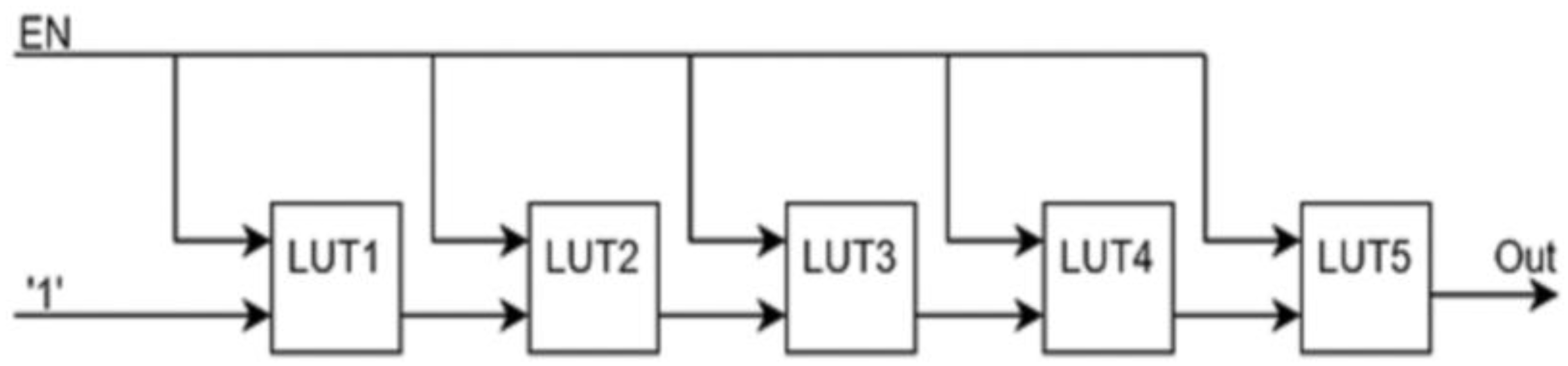
2.1. Architecture of Wave Union A TDCs

The WU-A launcher generates a finite number of transitions when the input level (hit signal) is ‘0’ and unleashes them through the TDC’s delay chain when the input level is ‘1’. WU-A architectures that generate the pulse patterns may be constructed based on carry multiplexers [27,28,29], look-up tables (LUTs) [30,31], or flip-flops (FFs) [19].
The LUTs on the Zynq system-on-chip FPGA on the ZED board served as the foundation for our suggested WU-A architecture. Two slices can be found in a single configurable logic block (CLB) of the Zynq 7000 series FPGAs. Each slice contains 8 FFs and 4 LUTs [32]. The number of inputs to the LUT and the logic functions it implements are user-configurable. The wave union A launcher was built using LUTs with specified values to generate two 1–0 transitions and one 0-1 transition, as illustrated in Figure 1. The LUTs were manually positioned in a slice near where the source of the hit signal is located.
Our TDC designed and built using a matrix of 1024 counters, with the routing paths serving as delay components [14]. The triggering signal that controls the pulse train’s creation and propagation is called the enable signal (EN). The architecture of the WU-A TDC is depicted in Figure 2. Our designed WU-A launcher sets up two 1–0 and one 0–1 transitions when EN is “0” and puts it on hold in the LUTs. When EN is “1”, the wave union propagates through the delay chain until the EN signal’s subsequent falling edge is reached. Of the three transitions, only the two 1–0 transitions are encoded. If one of the two transitions is missed due to it falling within an ultra-wide bin, the subsequent transition is likely to be recorded in the following clock cycle. As a result, the TDC becomes more sensitive and more linear.

2.2. Architecture of Wave Union B TDC

An infinite stream of pulses is produced by wave union launcher B [20,21]. As shown in Figure 3, it was constructed as a ring oscillator (ROC) using a buffer and a two-input NAND gate. Our proposed architecture for wave union launcher B was an NAND gate with an LUT programmed as a buffer. By increasing the number of LUTs in the feedback loop and adding more routing delays, the ring oscillator’s clock period can be adjusted. When the hit signal (EN) is ‘0’, the wave union launcher B’s output remains at a constant value of 1, and when it is ‘1’, it begins to oscillate.
Equation (1) provides a mathematical expression for the oscillation period ( T O S C ) of the launcher with K buffers in the feedback loop. The total delay comprises the propagation delay of the NAND gate ( t N A N D ), the routing path delay ( t r o u t ), and the delay of buffers ( t B u f f ).
T O S C 2 K t B u f f + t N A N D + t r o u t
The TDC’s clock period and the ROC’s period are intended to be similar. The TDC is based on a matrix of 1024 counters so that counters are sampled when the EN signal is ‘0’ and enabled when the EN input is ‘1’. Nonetheless, the ROC’s architecture is made such that, while EN is ‘0’, the output stays at a constant ‘1’, and, when EN is ‘1’, it begins to oscillate. This is not in line with the TDC’s architecture, which is built on a counter matrix. Consequently, we feed the ROC’s output to the counters’ EN inputs after inverting it. Figure 4 illustrates this.
The rising edge of the oscillation, or the 1–0 transitions, represents the pulse’s arrival time relative to the clock’s rising edge. We seek to quantify this phase difference as a new fine time. For a single measurement, the smallest arrival time that can be measured corresponds to the resolution (TLSB) of the TDC, which is ( T C L K /1024). Figure 5 shows the fine time, t i , measured on the ith clock cycle (i = 1, 2,...N) relative to the clock’s rising edge. The periodicity of t i can be mathematically expressed as in Equations (2) and (3) [21]:
t i = t i 1 + T O S C T C L K
t i = t 0 i + ( i 1 ) ( T O S C T C L K )
where t 0 i is the fine time corresponding to the first clock cycle, T O S C is the period of the ring oscillator, and T C L K is the reference clock period. Because of the disparities in ring oscillator and reference clock frequencies, cell delays can be efficiently partitioned, allowing for a denser redistribution of the tap delay in the 1024 fine-time interpolators. A multi-time averaging measurement is performed by capturing numerous pictures of the counters’ states over N-clock cycles. If the reference clock and ring oscillator frequencies are known, the matching values can be computed from any one of the TDC’s N-measured outputs. For a single-shot measurement, the final fine time is obtained by taking the average, as shown in Equation (4):
t 0 = 1 N i = 1 N t 0 i
Figure 5 shows the timing diagram for a single-shot measurement. The rising edge of the inverted wave union launcher output coincides with the rising edge of the EN signal. A four-bit gray code counter keeps track of the coarse time between the rising and falling edges of the EN signal. The fine-time interpolator delay chain is built with 1024 two-bit gray code counters. The ROC’s inverted output is launched through the delay chain, which is delayed by TLSB. Fine times in consecutive clock cycles are denoted as t1, t2,... tN. Combining Equations (3) and (4), the fine time, t 0 , can be redefined in terms of ti as in Equations (5)–(7).
t 0 = 1 N i = 1 N t i N 1 2 T O S C T C L K
t 0 = T C L K N × n i = 1 N j = 1 n K c l k , j , i N 1 2 T O S C T C L K
where K c l k , j , i is the output of the jth (j = 1, 2,... n) counter on the ith clock cycle. A multi-time averaging measurement allows us to measure finer time delays than n fine time interpolators. The resolution (TLSB) of the plain TDC is defined as T C L K n . The effective bin size, T e f f = TLSB/N, for the WU-B TDC is increased by N times, and its fine bins (Ceff) are uniformly dispersed among N × n unique integer values, as shown in Equation (6). Hence, the mathematical equation can be rewritten as in equation (7):
t 0 = T e f f × C e f f N 1 2 × ( T O S C T C L K )

3. Results and Discussion

The designed WU-A and WU-B TDCs are evaluated using a Zynq Evaluation and Development (ZED) board. An SR latch with two inputs obtained from clock sources from the FPGA’s phase-locked loop (PLL) is used to generate an EN signal. The two clocks that drive the S and R inputs of the SR latch have slipping frequencies, so the generated enable signal has a varying width that can cover the TDC’s dynamic range [14]. The ZED board FPGA and post-implementation schematics of the design exported from Vivado 2020.1 are shown in Figure 6a and Figure 6b, respectively.
The resources used, as reported by Vivado 2020.1 Xilinx ISE, are shown in Table 1. This table shows the resource utilization for both the WU-A and WU-B implementations. The extra cost of resources is for the implementation of the WU launchers. There is a slight increment in the percentage of slice LUTs used as logic elements in the WU-B TDC. The number of registers used and, as a result the number of slices utilized are slightly higher for the WU-A TDC. The percentages of utilized memory LUTs, block RAMs, and clock buffers remain the same for both WU-A and WU-B TDCs.
The power used by the system is the sum of its static and dynamic powers. Figure 7 shows the power report generated by Vivado 2020.1. A large fraction of the power dissipated is from the board’s processing system, which accounts for around 61% of the total power consumption for the WU-A TDC, as shown in Figure 7a, and 62% of total power consumption for the WU-B TDC, as shown in Figure 7b. The amount of power dissipated by the programmable logic is minimal in comparison with the power dissipated by the Zynq processor. According to Vivado 2020.1, the total on-chip power for WU-A is 2.684 W, while for WU-B it is 2.672 W. For both WU-A and WU-B TDCs, 93% of the total power consumption is dynamic power, whereas 7% is static power dissipation.

3.1. Stastical Results of WU-A TDC

Our standard TDC fine-time interpolator comprises 1024 counters with an EN input driven through a delay chain. Enough samples are collected, and the histogram can be generated by counting the number of hits in each bin. If you know the total number of counts, you can determine the bin width for each one. Over 500,000 total hits were taken to generate the histogram. Assuming the bins are evenly distributed during the TDC’s clock period of T C L K = 5.831 ns, the bin width for the ith bin with N number of counts is determined as in Equation (8).
B i n w i d t h i = N × T C L K t o t a l H i t s
Figure 8 depicts the bin width plot for the 1024 counters, derived from the plain TDC histogram. As illustrated in the figure, some bins are incredibly small (1 ps), and others are enormously large (12 ps). Most of the bins have an average size equal to the TDC’s resolution of 5.7 ps. The ultra-wide bins are generated by the long and slow routing wires that cross clock regions.
After applying the WU-A TDC, the ultra-wide bins were subdivided, and the TDC’s sensitivity improved significantly. The bin width distribution became uniform, as shown in Figure 9. The average bin width was still consistent with the TDC’s resolution of 5.7 ps.
The good impact on linearity can be noticed by comparing the transfer function of the ordinary TDC to the TDC with WUL-A. The transfer functions are obtained from the booked histograms. Figure 10 illustrates the transfer functions of the plain TDC and the TDC with WUL-A. It is demonstrated that the nonlinearity of the transfer function in the middle of the plot for the ordinary TDC (blue line plot) is improved when the WUL-A implementation is merged with the TDC (red line plot).

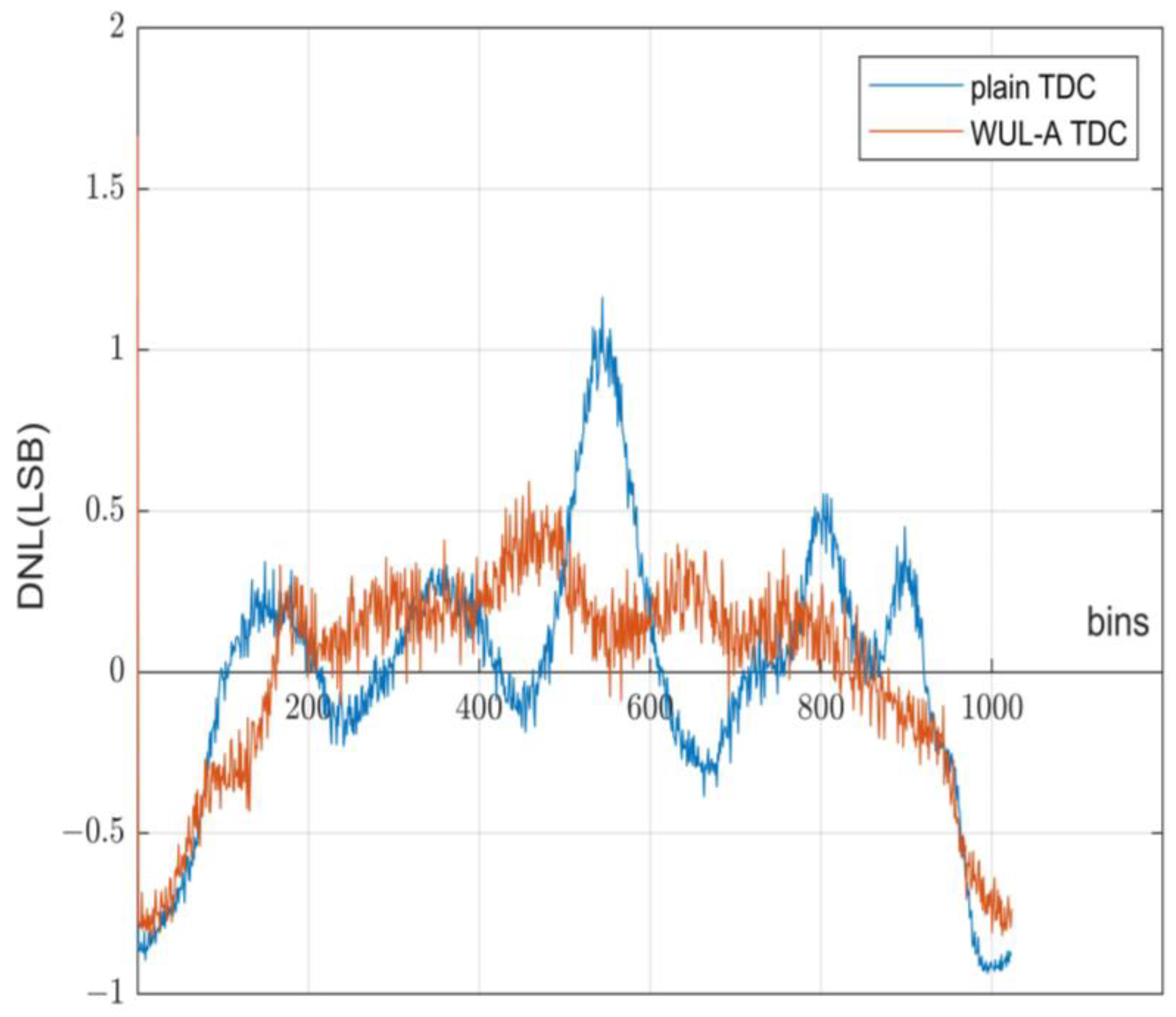
3.2. Differential and Integral Non-Linearity of WU-A TDC

The differential non-linearity (DNL) and integral non-linearity (INL) of the implemented TDC are calculated from the statistical data. Mathematically, the DNL of the ith bin can be written as in Equation (9):
D N L ( i ) = B i n w i d t h ( i ) L S B 1
where B i n w i d t h ( i ) is the bin size of the ith bin, as calculated in Equation (9), and LSB is the average bin size, also called the least significant bit, which is 5.7 ps. The INL is the integral of the DNL, as presented in Equation (10):
I N L ( i ) = j = 0 i 1 D N L ( j )
The plot in Figure 11 compares the DNL of the ordinary TDC and WU-A TDC. The root mean square (rms) DNL of the plain TDC is 0.41 LSB (2.31 ps), whereas the rms DNL of the WU-A TDC is 0.33 LSB (1.87 ps). The DNL of the WUL-A TDC (red line plot) improves by 19% when compared with the plain TDC (blue line plot).
The INL of the simple TDC, in contrast to the WU-A TDC, is depicted in Figure 12. The rms INL of the plain TDC is 2.61 LSB (14.86 ps), whereas the rms INL of the WU-A TDC is 1.12 LSB (6.36 ps). When WU-A is implemented, the INL improves significantly (57%).

3.3. Statistical Results of WU-B TDC

In WU-B implementation, the fine time is the phase of the ROC’s oscillation, determined by the arrival time of the EN signal relative to the next rising edge of the reference clock. A 4-bit coarse gray code counter sets the TDC’s measurement range as 16 × 5.831 ns = 93.296 ns. As a result, we can only take a maximum of 16 snapshots. The fine bins are dispersed in 16 × 1024 = 16,384 integers within a 5.831 ns clock period. The effective bin size, or the resolution of the WU-B TDC, is calculated as 5.831 ns/16,384 = 0.356 ps. By obtaining enough measurements, a realistic histogram for the WU-B TDC is created. The number of counts for each of the 16,384 bins is recorded, and the histogram is built.
The bin size for each bin is calculated using Equation (8). Figure 13 shows the bin size for each of the 16,384 bins, whereas Figure 14 depicts the distribution of the bin sizes. Many of the bins have a width of about 0.356 ps, which corresponds to the WU-B TDC resolution. Some bins are extremely small (0.016 ps), while others are extremely wide (1.5 ps).

3.4. Differential and Integral Non-Linearity of WU-B TDC

Equations (10) and (11) are used to determine the DNL and INL for the WU-B TDC. Figure 15 demonstrates that the DNL of the TDC ranges between +3.34 LSB (1.19 ps) and −0.98 LSB (−0.35 ps). The root mean square (RMS) for DNL is 0.60 LSB (0.21 ps).
The INL is depicted in Figure 16. The INL was between +6.01 LSB (2.17 ps) and −0.68 LSB (−0.24 ps). The RMS INL was reported to be 1.04 LSB (0.37 ps).

3.5. Comparison with Prior Works

Table 2 shows a comparison of the performance of our implemented WU-A and WU-B TDCs with earlier wave union implementations. Most of the wave union TDCs presented in Table 2 are based on carry chain delays in the FPGA, while our TDC is based on routing path delays as delay elements. A TDC with a 3.6 ps resolution was built by using WU-A with seven transitions [22]. The super wave union implementations carried out in [30,33] lead to high resolutions (0.9 ps and 1.17 ps, respectively) at the cost of extra resource utilization to build parallel delay lines and multiple wave union launchers. Our wave union A TDC uses two transitions and a single delay line to achieve a resolution of 5.7 ps. Although the resolution is not as good as that of the super wave union TDCs, our implementation is convenient for FPGA-based TDC designs in terms of resource utilization, and it leads to a substantial gain in linearity. A multisampling wave union approach where wave union launchers are applied at both the start and stop events is used in [23,34], where high resolutions (1.11 ps and 0.39 ps, respectively) are achieved compared with our 5.7 ps resolution WU-A TDC. However, the tradeoff between resolution and linearity can be observed by comparing the reported DNL and INL in [23], which are 4 LSB and 50 LSB, respectively, and the DNL and INL of our WU-A TDC, which are 0.5 LSB and 5 LSB, respectively.
The WU-B TDC has not been used extensively. The study in [21] used WU-B with four snapshots to produce a 12 ps resolution with a DNL of 1.1 LSB and an INL of 8 LSB. In our study, we used 16 measurements to achieve a 0.356 ps resolution with a DNL (rms) of 0.6024 LSB and an INL (rms) of 1.0383 LSB. Our WU-B TDC implementation improves the resolution from 12 ps to 0.356 ps, but the conversion speed is four times slower compared with that in the work in [21].

4. Conclusions

A low-cost Xilinx Zynq-7000 all-programmable system-on-chip (AP-SOC) with 28 nm CMOS technology FPGA was used to create a high-performance wave union time-to-digital converter based on a matrix of 1024 counters. The synthesis and implementation of the design were controlled by manual placement and routing constraints. The goal of the study was to increase the linearity and resolution of the TDC. The TDC’s sensitivity was further improved by using a LUT-based WU launcher A that generated a pulse train of one 0–1 and two 1–0 transitions. The WU-A TDC improves the DNL by 19% and the INL by 57% when compared with the regular TDC. This demonstrates that using the wave union approach to TDCs realized with routing path delays as delay factors results in a significant improvement in linearity.
The WU-B TDC enhances the fine-time measurement by a factor of 1/16. Despite the significant increase in resolution, the WU-B TDC’s linearity is limited to a DNL (rms) of 0.60 LSB and an INL (rms) of 1.04 LSB. The results indicate that using the WU-B TDC increases the resolution but reduces the differential linearity when compared with the WU-A TDC. In conclusion, the WU-A TDC has the best linearity, whereas the WU-B TDC results in a higher resolution. However, the performance of the WU-B TDC is limited by the conversion speed or its dead time. If we increase the number of multiple measurements taken, we can achieve higher resolution, but the conversion speed degrades. For applications that need a fast conversion speed, the trade-off between resolution and conversion speed should be considered.
In the future, WU-A TDC implementations with more than two transitions can be investigated to see if they improve linearity relative to the resource overhead they bring. A multi-edge wave union approach where the WU-A launcher is used on the rising edge of the EN signal and the WU-B launcher is used on the falling edge of the EN signal may subdivide the ultra-wide bins present in the WU-B TDC and lead to improved DNL.

Author Contributions

Conceptualization R.T.S.; methodology, R.T.S., J.P. and P.L.; software, R.T.S.; validation, R.T.S., J.P. and P.L.; formal analysis, R.T.S.; investigation, R.T.S.; resources, R.T.S., J.P. and P.L.; writing—original draft preparation, R.T.S.; writing—review and editing, R.T.S., G.A., J.P. and P.L.; supervision, G.A., J.P. and P.L.; project administration, G.A., J.P. and P.L. All authors have read and agreed to the published version of the manuscript.

Funding

This research was supported by the Home-Grown Ph.D. Program (HGPP) funded by the Ethiopian Ministry of Education.

Data Availability Statement

Data are contained within the article.

Conflicts of Interest

The authors declare no conflicts of interest.

References

  1. Korkan, A.O.; Yuksel, H. A Novel Time-to-Amplitude Converter and a Low-Cost Wide Dynamic Range FPGA TDC for LiDAR Application. IEEE Trans. Instrum. Meas. 2022, 71, 2005015. [Google Scholar] [CrossRef]
  2. Xie, W.; Chen, H.; Zang, Z.; Li, D.D.U. Multi-channel high-linearity time-to-digital converters in 20 nm and 28 nm FPGAs for LiDAR applications. In Proceedings of the 2020 6th International Conference on Event-Based Control, Communication, and Signal Processing (EBCCSP), Krakow, Poland, 23–25 September 2020; pp. 4–7. [Google Scholar] [CrossRef]
  3. Jee, D.W.; Seo, Y.H.; Park, H.J.; Sim, J.Y. A 2 GHz fractional-N digital PLL with 1b noise shaping ΔΣ TDC. IEEE J. Solid-State Circuits 2012, 47, 875–883. [Google Scholar] [CrossRef]
  4. Gao, W.; Gao, D.; Guo, C.H.; Hu, Y. Time-to-Digital Converters (TDCs) for PET Imaging. In Biomedical Engineering, Trends in Electronics, Communications and Software; Laskovski, A.N., Ed.; IntechOpen: London, UK, 2009. [Google Scholar]
  5. Lecoq, P. Pushing the Limits in Time-of-Flight PET Imaging. IEEE Trans. Radiat. Plasma Med. Sci. 2017, 1, 473–485. [Google Scholar] [CrossRef]
  6. Wang, Y.; Xie, W.; Chen, H.; Day-Uei Li, D. High-resolution time-to-digital converters (TDCs) with a bidirectional encoder. Meas. J. Int. Meas. Confed. 2023, 206, 112258. [Google Scholar] [CrossRef]
  7. Dikopoulos, E.; Birbas, M.; Birbas, A. An Adaptive Downsampling FPGA-Based TDC Implementation for Time Measurement Improvement. Chips 2022, 1, 175–190. [Google Scholar] [CrossRef]
  8. Tontini, A.; Gasparini, L.; Pancheri, L.; Passerone, R. Design and Characterization of a Low-Cost FPGA-Based TDC. IEEE Trans. Nucl. Sci. 2018, 65, 680–690. [Google Scholar] [CrossRef]
  9. Fishburn, M.W.; Menninga, L.H.; Favi, C.; Charbon, E. A 19.6 ps, FPGA-based TDC with multiple channels for open source applications. IEEE Trans. Nucl. Sci. 2013, 60, 2203–2208. [Google Scholar] [CrossRef]
  10. Lai, J.; Luo, Y.; Shao, Q.; Bao, L.; Liu, X. A high-resolution TDC implemented in a 90nm process FPGA. In Proceedings of the International Conference on ASIC, Shenzhen, China, 28–31 October 2013; pp. 2–4. [Google Scholar] [CrossRef]
  11. Kwiatkowski, P. Employing FPGA DSP blocks for time-to-digital conversion. Metrol. Meas. Syst. 2019, 26, 631–643. [Google Scholar] [CrossRef]
  12. Wang, H.; Zhang, M.; Yao, Q. A new realization of time-to-digital converters based on FPGA internal routing resources. IEEE Trans. Ultrason. Ferroelectr. Freq. Control 2013, 60, 1787–1795. [Google Scholar] [CrossRef]
  13. Zhang, M.; Wang, H.; Liu, Y. A 7.4 ps FPGA-based TDC with a 1024-unit measurement matrix. Sensors 2017, 17, 865. [Google Scholar] [CrossRef]
  14. Siecha, R.T.; Alemu, G.; Prinzie, J.; Leroux, P. 5.7 ps Resolution Time-to-Digital Converter Implementation Using Routing Path Delays. Electronics 2023, 12, 3478. [Google Scholar] [CrossRef]
  15. Dudek, P.; Szczepański, S.; Hatfield, J.V. A high-resolution CMOS time-to-digital converter utilizing a Vernier delay line. IEEE J. Solid-State Circuits 2000, 35, 240–247. [Google Scholar] [CrossRef]
  16. Cui, K.; Li, X. A high-linearity vernier time-to-digital converter on FPGAs with improved resolution using bidirectional-operating vernier delay lines. IEEE Trans. Instrum. Meas. 2020, 69, 5941–5949. [Google Scholar] [CrossRef]
  17. Cui, K.; Li, X.; Liu, Z.; Zhu, R. Toward Implementing Multichannels, Ring-Oscillator-Based, Vernier Time-to-Digital Converter in FPGAs: Key Design Points and Construction Method. IEEE Trans. Radiat. Plasma Med. Sci. 2017, 1, 391–399. [Google Scholar] [CrossRef]
  18. Shen, Q.; Liu, S.; Qi, B.; An, Q.; Liao, S.; Shang, P.; Peng, C.; Liu, W. A 1.7 ps equivalent bin size and 4.2 ps RMS FPGA TDC based on multichain measurements averaging method. IEEE Trans. Nucl. Sci. 2015, 62, 947–954. [Google Scholar] [CrossRef]
  19. Liu, C.; Wang, Y. A 128-channel, 710 M samples/second, and less than 10 ps RMS resolution time-to-digital converter implemented in a kintex-7 FPGA. IEEE Trans. Nucl. Sci. 2015, 62, 773–783. [Google Scholar] [CrossRef]
  20. Wu, J.; Shi, Z. The 10-ps wave union TDC: Improving FPGA TDC resolution beyond its cell delay. IEEE Nucl. Sci. Symp. Conf. Rec. 2008, 1, 3440–3446. [Google Scholar] [CrossRef]
  21. Wang, J.; Liu, S.; Zhao, L.; Hu, X.; An, Q. The 10-ps multitime measurements averaging TDC implemented in an FPGA. IEEE Trans. Nucl. Sci. 2011, 58, 2011–2018. [Google Scholar] [CrossRef]
  22. Bayer, E.; Zipf, P.; Traxler, M. A multichannel high-resolution (<5 ps RMS between two channels) time-to-digital converter (TDC) implemented in a field programmable gate array (FPGA). In Proceedings of the IEEE Nuclear Science Symposium Conference Record, Valencia, Spain, 23–29 October 2011; pp. 876–879. [Google Scholar] [CrossRef]
  23. Kwiatkowski, P.; Szplet, R. Efficient Implementation of Multiple Time Coding Lines-Based TDC in an FPGA Device. IEEE Trans. Instrum. Meas. 2020, 69, 7353–7364. [Google Scholar] [CrossRef]
  24. Kwiatkowski, P.; Sondej, D.; Szplet, R. A brief review of wave union TDCs. In Proceedings of the EBCCSP 2021—7th International Conference on Event-Based Control, Communication, and Signal Processing, Krakow, Poland, 22–25 June 2021; pp. 1–6. [Google Scholar] [CrossRef]
  25. Avnet Electronics Marketing. ZedBoard ZynqTM Evaluation and Development Hardware User’s Guide. 2012. Available online: https://digilent.com/reference/_media/zedboard:zedboard_ug.pdf (accessed on 12 April 2024).
  26. Travaglini, R.; Antone, I.D.; Meneghini, S.; Rignanese, L.; Zu, M. Design and implementation of projects with Xilinx Zynq FPGA: A practical case. Mem. Della Soc. Astron. Ital. 2017, 88, 186–194. [Google Scholar]
  27. Wang, Y.; Liu, C. A 3.9 ps Time-Interval RMS Precision Time-to-Digital Converter Using a Dual-Sampling Method in an UltraScale FPGA. IEEE Trans. Nucl. Sci. 2016, 63, 2617–2621. [Google Scholar] [CrossRef]
  28. Wang, Y.; Zhou, X.; Song, Z.; Kuang, J.; Cao, Q. A 3.0-ps rms Precision 277-MSamples/s Throughput Time-to-Digital Converter Using Multi-Edge Encoding Scheme in a Kintex-7 FPGA. IEEE Trans. Nucl. Sci. 2019, 66, 2275–2281. [Google Scholar] [CrossRef]
  29. Alshahry, S.M.; Alshehry, A.H.; Alhazmi, A.K.; Chodavarapu, V.P. A Size, Weight, Power, and Cost-Efficient 32-Channel Time to Digital Converter Using a Novel Wave Union Method. Sensors 2023, 23, 6621. [Google Scholar] [CrossRef] [PubMed]
  30. Szplet, R.; Sondej, D.; Grzȩda, G. High-Precision Time Digitizer Based on Multiedge Coding in Independent Coding Lines. IEEE Trans. Instrum. Meas. 2016, 65, 1884–1894. [Google Scholar] [CrossRef]
  31. Lusardi, N.; Garzetti, F.; Geraci, A. Digital instrument with configurable hardware and firmware for multi-channel time measures. Rev. Sci. Instrum. 2019, 90, 055113. [Google Scholar] [CrossRef] [PubMed]
  32. Xilinx Inc. Zynq-7000 SoC Data Sheet: Overview. Xilinx 2018, DS190, 1–21. [Google Scholar]
  33. Lusardi, N.; Garzetti, F.; Corna, N.; De Marco, R.; Geraci, A. Very High-Performance 24-Channels Time-to-Digital Converter in Xilinx 20-nm Kintex UltraScale FPGA. In Proceedings of the 2019 IEEE Nuclear Science Symposium and Medical Imaging Conference (NSS/MIC), Manchester, UK, 26 October–2 November 2019; pp. 5–8. [Google Scholar] [CrossRef]
  34. Xie, W.; Chen, H.; Li, D.D.U. Efficient Time-to-Digital Converters in 20 nm FPGAs with Wave Union Methods. IEEE Trans. Ind. Electron. 2022, 69, 1021–1031. [Google Scholar] [CrossRef]
  35. Kwiatkowski, P.; Sondej, D.; Szplet, R. Bubble-proof algorithm for wave union tdcs. Electronics 2022, 11, 30. [Google Scholar] [CrossRef]
Figure 1. Look-up table-based WU-A launcher implementation.
Electronics 13 02359 g001
Figure 2. Architecture of WU-A TDC.
Electronics 13 02359 g002
Figure 3. Architecture of wave union launcher B.
Electronics 13 02359 g003
Figure 4. The WU-B TDC architecture.
Electronics 13 02359 g004
Figure 5. Timing diagram for WU-B TDC.
Electronics 13 02359 g005
Figure 6. (a) Zynq Evaluation and Development board. (b) WU-TDC after post placement and implementation.
Electronics 13 02359 g006
Figure 7. Power dissipated by (a) WU-A TDC (b) WU-B TDC.
Electronics 13 02359 g007aElectronics 13 02359 g007b
Figure 8. Bin size: 1024-unit TDC.
Electronics 13 02359 g008
Figure 9. Bin size of plain TDC versus WU-A TDC.
Electronics 13 02359 g009
Figure 10. Transfer function of plain TDC versus WU-A TDC.
Electronics 13 02359 g010
Figure 11. Differential non-linearity of plain TDC versus WU-A TDC.
Electronics 13 02359 g011
Figure 12. Integral non-linearity of plain TDC versus WU-A TDC.
Electronics 13 02359 g012
Figure 13. Bin size for 16,384 bins for the WU-B time-to-digital converter.
Electronics 13 02359 g013
Figure 14. Histogram of the bin size distribution.
Electronics 13 02359 g014
Figure 15. Differential non-linearity for the WU-B time-to-digital converter.
Electronics 13 02359 g015
Figure 16. Integral non-linearity of WU-B time-to-digital converter.
Electronics 13 02359 g016
Table 1. Resource utilization report for WU-TDCs.
WU-A (1024 Counter Matrix)WU-B (1024 Counter Matrix)
AvailableUsedUtilization (%)UsedUtilization (%)
Slice Registers106,40051,21448.1351,19348.11
Slice LUTs53,20030,35957.0730,39257.13
LUTs as logic53,20019,05935.8319,09235.89
LUTs as memory17,40011,30064.9411,30064.94
Slices13,30012,68295.3512,60394.76
Block RAM14064.546.0764.546.07
BUFGCTRL32721.88721.88
MMCME2-ADV4375375
Table 2. Comparison of wave union TDCs.
WorkMethod TechnologyBinsLSB (ps)DNL (LSB)INL (LSB)
[20] (2008)WU-A
WU-B
90 nm6430
-
-
-
-
-
[21] (2011)WU-B90 nm830121.18
[22] (2011)WU-A90 nm2563.6--
[30] (2016)Super WU-A 45 nm21760.9-−26.2
[33] (2019)Super WU-A20 nm81921.17--
[28] (2019)WU-A28 nm10181.774.5−37.7
[23] (2020)Multi-sampling WU-A28 nm15001.11450
[34] (2022)WU-A20 nm7901.23–2.531.755.97
[35] (2021)Multi-sampling WU-A and WU-B28 nm2000.39--
This workWU-A28 nm10245.70.33 (RMS)1.12 (RMS)
WU-B 16,3840.3560.60 (RMS)1.04 (RMS)
Disclaimer/Publisher’s Note: The statements, opinions and data contained in all publications are solely those of the individual author(s) and contributor(s) and not of MDPI and/or the editor(s). MDPI and/or the editor(s) disclaim responsibility for any injury to people or property resulting from any ideas, methods, instructions or products referred to in the content.

