Article

Compact Internally Matched High-Power Power Amplifier with a Wide Frequency Band of 0.8–2 GHz

1
Yangtze Delta Region Institute (Huzhou), University of Electronic Science and Technology of China, Huzhou 313001, China
2
School of Electronic Science and Engineering, University of Electronic Science and Technology of China, No. 2006, Xiyuan Ave, West Hi-Tech Zone, Chengdu 611731, China
3
Dynax Semiconductor Inc., Suzhou 215300, China
*
Author to whom correspondence should be addressed.
Electronics 2024, 13(14), 2687; https://doi.org/10.3390/electronics13142687
Submission received: 13 June 2024 / Revised: 1 July 2024 / Accepted: 4 July 2024 / Published: 9 July 2024
(This article belongs to the Section Microwave and Wireless Communications)

Abstract

:
In this paper, a GaN high-electron-mobility transistor (HEMT) compact high-power wide-band power amplifier with an operation frequency from 0.8 GHz to 2 GHz is proposed. In order to realize a compact design, an internally matched method is employed. A wide-band matching strategy with an LC network and a multi-stage wide-band power combiner/divider is introduced in this design to achieve a wide bandwidth. A power combination structure is applied to have high output power. Wire-spiral inductance and film capacitors are employed to construct the compact matching network. The equivalent inductance of the bonding wire is also involved in the matching network. Experimental results show that the PAE (power-added efficiency) during the whole operation’s bandwidth (0.8 GHz to 2.0 GHz) is from 40% to 57%. The output power can reach from 48.3 dBm to 49.8 dBm with a circuit size of 30.8 × 27.4 mm 2 .

1. Introduction

As electronic warfare systems evolve, the quest for higher-power density and broader-frequency band coverage has become paramount [1]. These advancements are critical in enhancing the system’s capabilities and effectiveness in modern warfare scenarios. Thus, electronic warfare systems urgently need power amplifiers that offer high-power output, a miniaturized circuit size, and wide bandwidths.
The size of the power amplifier circuit is one of its important parameter indicators. Traditional externally matched PA can achieve high power and efficiency easily, but the shortcoming is the circuit size. A monolithic Microwave Integrated Circuit (MMIC) power amplifier is a PA integrated on a single semiconductor chip, characterized by its miniaturization and high integration [2]. However, the manufacturing process of MMIC power amplifiers is complex and costly, and their power output and efficiency are inferior to those of traditional externally matched power amplifiers. Therefore, researchers have proposed internally matching power amplifiers with a high dielectric constant and high-thermal-conductivity dielectric substrates as well as gold-wire bonding technology [3,4]. Such a power amplifier can achieve similar power and efficiency to a traditional externally matched power amplifier in a very small area.
To expand the bandwidth of power amplifiers (PAs), researchers have proposed various schemes, including distributed [5,6], feedback [7,8], balanced [9,10,11], resistance–reactance, etc., which have garnered increased attention over the past decade. While distributed, balanced, and feedback circuit structures can effectively broaden bandwidth, they often result in decreased amplifier gain due to their mutual constraint relationship with bandwidth. Moreover, these structures may reduce amplifier efficiency and introduce parasitic elements and circuit complexity. Recently, there has been a proposal for expanding the bandwidth of continuous mode amplifiers such as continuous class E [12], continuous class F [13], and continuous class F 1 [14]. These continuous-class power amplifiers introduce correction factors into current or voltage equations at the drain terminal to provide one or more sets of fundamental wave impedance solutions that enhance design flexibility for matching networks and that facilitate frequency band expansion. However, continuous power amplifiers are typically more complex and only suitable for medium-power transistors.
The resistance–reactance amplifier primarily compensates for transistor gain rolling characteristics using matching networks composed of resistance–reactance components to achieve in-band flatness requirements. This wide-band matching method is structurally simple yet capable of delivering high output power and efficiency.
To fulfill the demand for high power, wide bandwidth, and small circuit size of electronic warfare systems, internal matching techniques have been adopted based on reactive matching in this paper. Our main contribution is that the high power and wide bandwidth are simultaneously achieved by step-by-step wide-band matching and power combination in a very small circuit size. The input and output matching networks are analyzed and implemented with the LC network and with the transmission line, which is part of the power combiner. Furthermore, an equivalent circuit model is proposed to simulate the wire-spiral inductor for accurate circuit design. Finally, experimental measurements are conducted to verify the performance of the proposed PA.

2. Design of Proposed Compact Wide-Band PA

2.1. Overall Design

Figure 1 shows the schematic diagram of the proposed 0.8–2.0 GHz internally matched PA. This frequency range can cover part of radar and communication systems, which are both targets of an electronic warfare system. To achieve the required output power of the power amplifier within a small size, the design in this paper greatly reduces the area of the circuit by using alumina with high permittivity as the substrate and achieving the required output power by adopting the power combination method. Because of the high permittivity of the alumina substrate, the quarter wavelength line has a smaller size than externally matched PAs. The thermal conductivity of the alumina substrate also provides a foundation for high-power output. Thus, an internally matched method can achieve a small circuit size and high output power simultaneously. The employed HEMT is manufactured by the 0.25 μ m process from Dynax Semiconductor Inc., which has a drain source breakdown voltage of 150 V. The size of the HEMT is 655 × 2725 × 100 μ m. In order to ensure the operating bandwidth of the power amplifier, a high-order broadband power divider/combiner, and a broadband step-matching network are adopted for input and output matching. The power divider/combiner has the function of impedance transformation by using micro-strip lines with different characteristics of impedance. The matching circuit employs gold wire bonding, thin-film capacitors, and thin-wire-spiral inductance inductors to achieve matching while utilizing numerous bent micro-strip line structures. This significantly reduces the circuit size, enabling the entire circuit to be encapsulated in a single tube, thus realizing an internally matched power amplifier.

2.2. Impedance Choosing

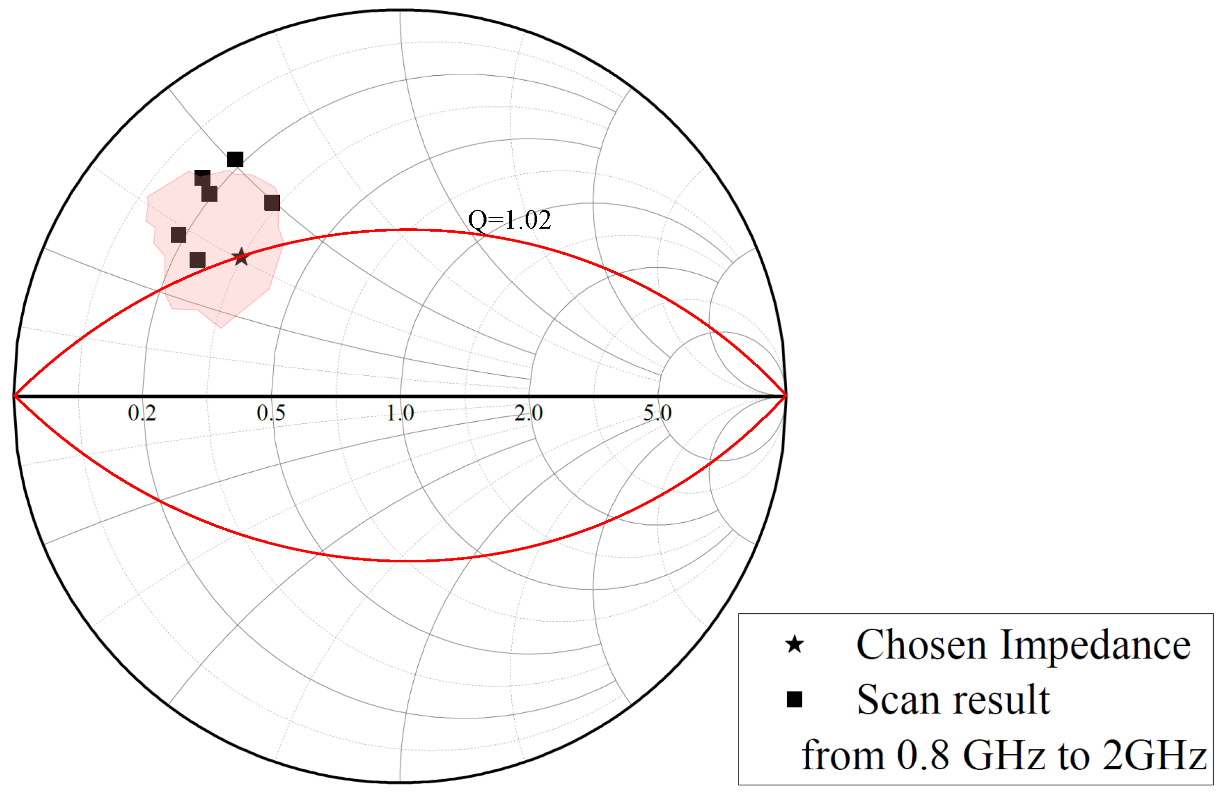
The target operating bandwidth is from 0.8 GHz to 2.0 GHz. Firstly, the load-pull and source-pull simulations are implemented to search for the best matching load. The load-pull and results of best PAE from 0.8 GHz to 2.0 GHz are given in Figure 2.
A traditional way to choose matching impedance is to directly use the best impedance of the middle-frequency: 1.4 GHz. However, we have to consider the difficulty when designing the matching network. Since the bandwidth of each part of the PA circuit can affect the final operation bandwidth of the PA, the impedance should be chosen for an easier design of the matching network. The quality factor (Q factor) should be carefully considered. The relationship of operation bandwidth, Q factor (quality factor), and impedance is given in Equation (1):
Q = I m Z R e Z = f 0 Δ f
A higher Q factor means narrow bandwidth and low loss, while a lower Q factor means wide bandwidth and more loss. To extend the operation bandwidth, a trade-off of output power, PAE, and Q is performed. The impedance of the input and output matching network should be chosen more easily by a low Q factor matching network. But the impedance should not leave the high PAE zone, which is given in the red area in Figure 2. The chosen out-matching impedance is 16.6 + 17j Ω . A similar process is performed for input matching impedance. The input matching impedance is 8.14 + 5.4j Ω .

2.3. Input Matching Network Design

To expand the operation bandwidth, a step-by-step matching method is implemented in the input matching network design. There is a middle impedance between the ideal matching impedance and 50 Ω . This process can help to reduce the Q factor when matching with an inductor–capacitor network. The middle impedance is chosen as 12.5 Ω . The input matching network is designed to match from 12.5 Ω to the ideal impedance (8.14 + 5.4j Ω ) by an inductor–capacitor network. Then, the matching to 50 Ω is performed by the power divider.
A schematic diagram of the input matching network and layout of the LC input matching network is shown in Figure 3. L 1 is the equivalent inductance of a set of gold bonding wires, where the typical value of inductance is 200 pH. C 1 = 8.1 pf is implemented by a film capacitor whose size is 2.2 × 0.18 × 0.19 mm. It can be seen in Figure 3 that there are four small pads for tuning the value of L 1 . L 2 = 1.3 nH, which is implemented by the spiral inductor. The wire-spiral inductance is implemented by a transmission line, which is made by gold. Under the gold layer, there is a layer of nickel that is used to assist in welding it onto the substrate. And the size of L2 is 2 × 0.4 × 0.254 mm. The circuit components are connected by gold bonding wire. The LC network transforms the impedance from 12.5 Ω to the ideal input conjugate impedance 8.14 − 5.4j Ω . The remaining two λ / 4 micro-strip lines are part of the power divider. The different characteristic impedances make the bandwidth of the impedance transformation circuit wider, which will be further discussed in the following section. The characteristic impedance of Z 1 is 33 Ω . The characteristic impedance of Z 2 is 16 Ω .
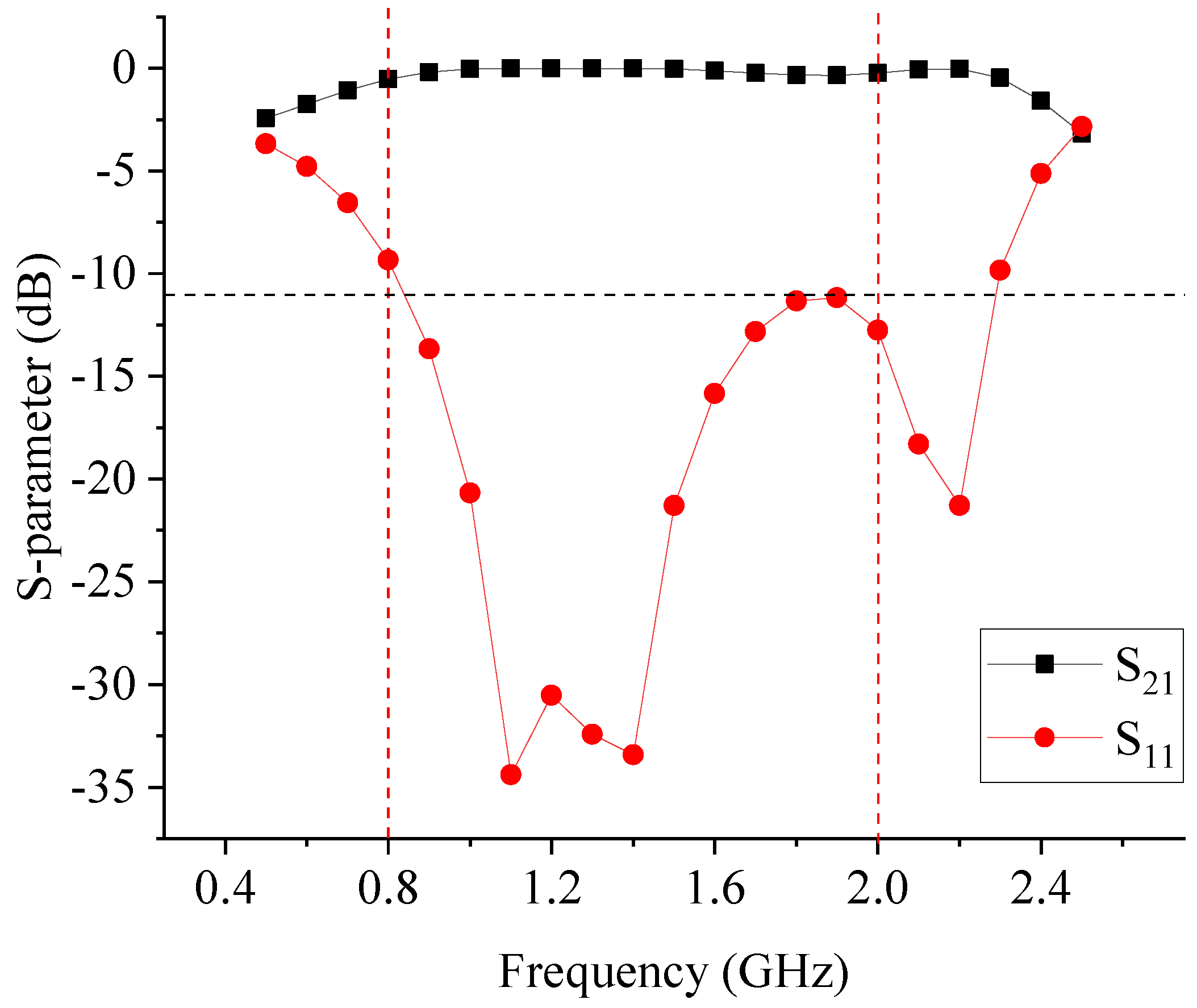
The proposed input matching network is simulated between terms from 50 Ω to 8.14 − 5.4j Ω . The simulation result is shown in Figure 4. It can be seen from Figure 4 that the pass band of the matching network is wide enough to cover the operation bandwidth from 0.8 GHz to 2.0 GHz. The insert loss is lower than −0.3 dB during the whole operation bandwidth.

2.4. Out-Matching Network Design

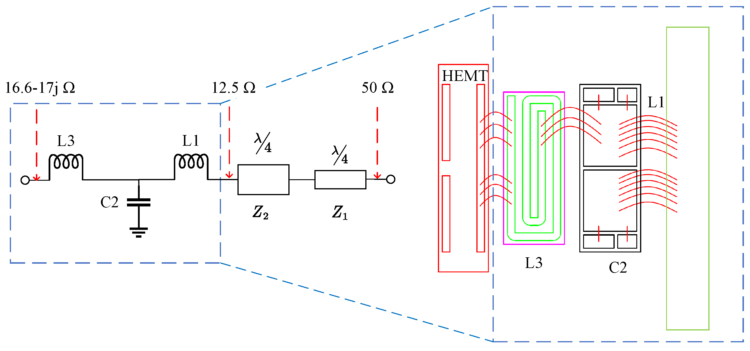
The out-matching network is similar to the input matching network. The three-step matching strategy is also implemented. The schematic diagram of the outmatching network is given in Figure 5. The L-C network firstly transforms the impedance from the ideal output match load (16.6 − 17j Ω ) to a middle value 12.5 Ω . L 3 = 1.7 nH is a spiral inductance. The bonding wire can be connected at different places of L3 to tune the value of L3. The size of L3 is 2 × 0.8 × 0.254 mm. The total size of film capacitor C2 is 2.2 × 0.18 × 0.19 mm. The value of C2 can be chosen by connecting different pads of C2. The value of C2 is 1 pf. L 1 = 200 pH is a typical inductance from the set of gold bonding wires. Then, the two micro-strip lines with λ / 4 wavelength transform the impedance to 50 Ω . The characteristic impedance of Z 1 and Z 2 are 33 Ω and 16 Ω , respectively. The two micro-strip lines are also part of the power combiner at the output of the PA.
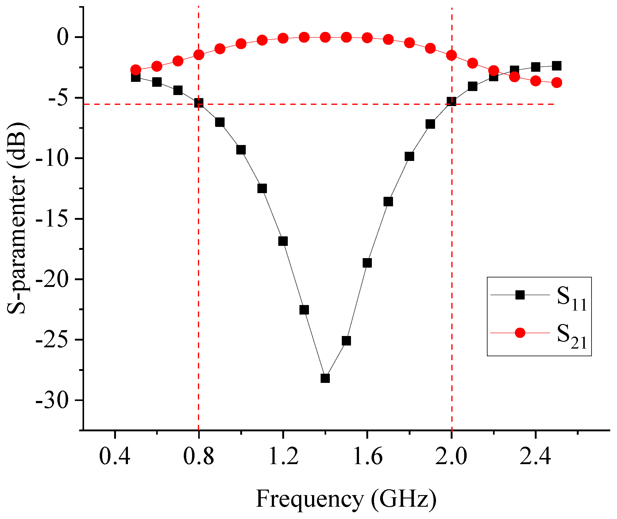
The simulation result of the output matching network is given in Figure 6. The simulation terms are the objective load matching impedance. Both S11 and S21 show a good operation frequency bandwidth from 0.8 GHz to 2 GHz. S21 is larger than −1.5 dB during the whole objective frequency range.

2.5. Analysis of Wire-Spiral Inductor

The equivalent inductance of the gold wire can be calculated using the equation:
L = 1 2 π f Im Y 1 , 1
where the Im Y 1 , 1 represents the imaginary part of the Y 1 , 1 parameter and f is the working frequency. Due to the large inductance of L2, the composite structure of the gold-bonding-wire-spiral inductor is used to achieve this large inductance. However, this composite structure brings great difficulty to circuit simulation. The traditional parameter extraction method of the gold bonding wire and spiral inductance discrete model neglects the discontinuity of the connection, resulting in insufficient simulation accuracy after the cascade. To improve the simulation accuracy of the composite structure, an equivalent circuit model of the gold-bonding-wire-spiral inductor composite containing the location information of the access point of the gold bonding wire is proposed.
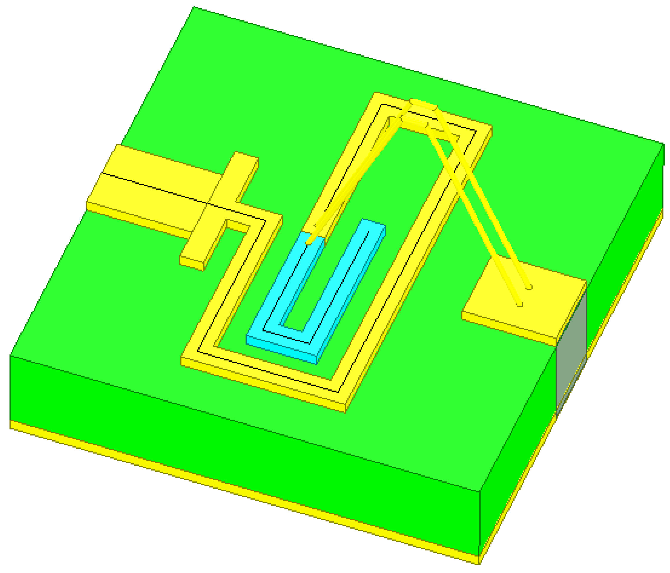
Figure 7 is the schematic diagram of the gold-bonding-wire-spiral inductor composite structure. The bonding point of gold bonding wire divides the spiral inductor into two sections: the accessed part and the unaccessed part. The position of the access point determines the length of the two sections to realize different access inductors. The gold part is the accessed part, and the blue part is the unaccessed part.
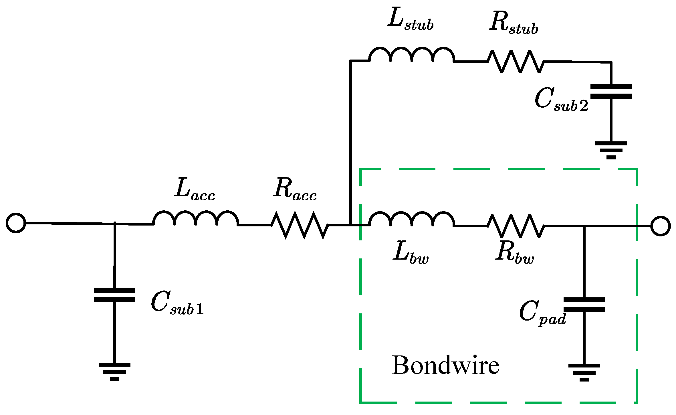
Figure 8 shows the equivalent circuit model of the gold-bonding-wire-spiral inductor composite structure. The inside of the green box is the equivalent circuit of the gold bonding wire part, and the outside is the spiral-inductor part. L a c c and R a c c represent the inductance and resistance of the accessed circuit part (yellow); L s t u b and R s t u b represent the inductance and resistance of the unaccessed circuit part (blue); L b w and R b w represent the inductance and resistance of the gold bonding wire part; and C s u b represents the dielectric capacitance of each segment. C p a d is the ground capacitance of the output pad. The equivalent circuit model of the gold-bonding-wire-spiral inductor composite structure has successfully realized the precise representation of the gold-bonding-wire-spiral inductor composite structure, so the equivalent circuit model can be used in the simulation of the internally matched power amplifier. Capacitor C is realized by thin-film circuit technology, and the substrate material is alumina ceramics with a relative dielectric constant of 9.9. The capacitance value of the parallel plate capacitor can be calculated by Equation (3):
C = ε 0 ε r d A d = ε 0 ε r d W · l d
where W and l, respectively, represent the width and length of the parallel plate capacitor; ε r d represents the dielectric constant of the medium parallel plate capacitor; and ε 0 represents the dielectric constant of the vacuum.

2.6. Design of Power Divider/Combiner

As introduced in the last two sections, the power divider/combiner has the function of impedance transformation as well as the power combined and power divided. The wide-band structure with two micro-strip lines is derived from a multi-stage wide-band Wilkinson power divider.
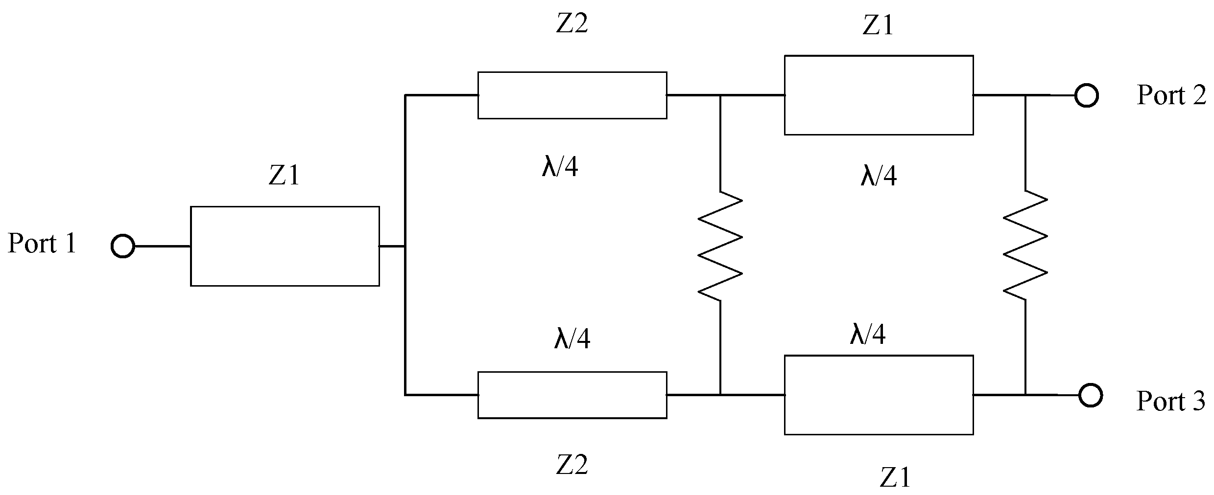
Figure 3 illustrates the basic circuit structure of a two-stage Wilkinson power divider, consisting of two power division branches and two isolation resistors. Each power division branch is composed of two sections of transmission lines with a length of λ / 4 , and each section has different characteristic impedances Z1 and Z2. Therefore, an impedance discontinuity is formed at the junction of each transmission line section. According to the theory of small reflections, the total reflected wave at the input port can be approximately viewed as the superposition of the reflected waves at each discontinuity as given in Equation (4):
Γ = Γ 1 + Γ 2 + + Γ n
The traditional Wilkinson power divider structure only contains one λ / 4 impedance transformation line and two impedance discontinuities, where the reflected waves are canceled only at the frequency corresponding to one-quarter of the operating wavelength, resulting in a narrow matching bandwidth. When multiple Wilkinson power divider structures are cascaded, the number of discontinuities increases and more reflected waves superimpose at the input port, enabling the reflected waves to be canceled at multiple frequency points. This is why a two-stage Wilkinson power divider can have a wide bandwidth [15,16].
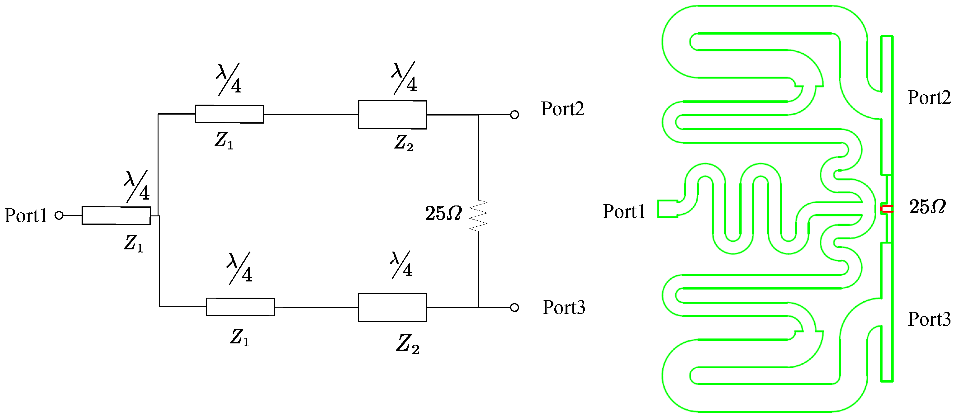
When considering transforming the impedance to another value between the ideal impedance of the matching network, the micro-strip lines with characteristic impedance Z 2 and Z 1 in the right part in Figure 9 should be changed to Z 1 and Z 2 . The isolation resistor in the middle is removed for a compact layout design. Since the impedance at port 2 and port 3 have been changed to 12.5 Ω , the isolation resistor value is set to 25 Ω . Then, the structure of the power divider/combiner is changed into the structure as shown in Figure 10. Figure 10 also gives the layout of the power divider. To minimize the circuit size, the layout design of the power divider/combiner incorporates a large number of bends.
The simulation result of the power divider/combiner is given in Figure 11. The power divider/combiner satisfies the reciprocity theorem. S12 and S11 are given in Figure 11. It can be seen that the power divider/combiner can achieve a wide bandwidth from 0.8 GHz to 2.0 GHz. Since the structure of PA is balanced with the same circuit design, the isolation performance is not very important in this design.

3. Results and Discussion

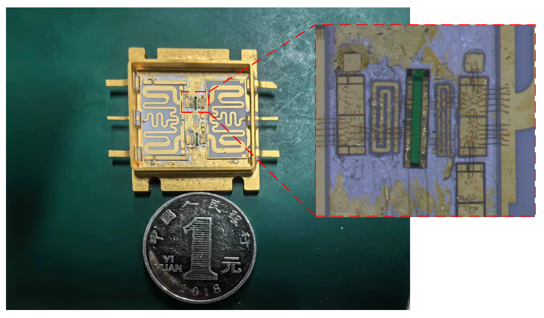
The proposed internally matched wide-band PA is implemented by using alumina with high permittivity as the substrate. So, the circuit size can be small enough to be encapsulated in a package. A photo of the proposed PA is given in Figure 12. The total size of the package is 30.8 × 27.4 mm 2 .

3.1. Small Signal Test

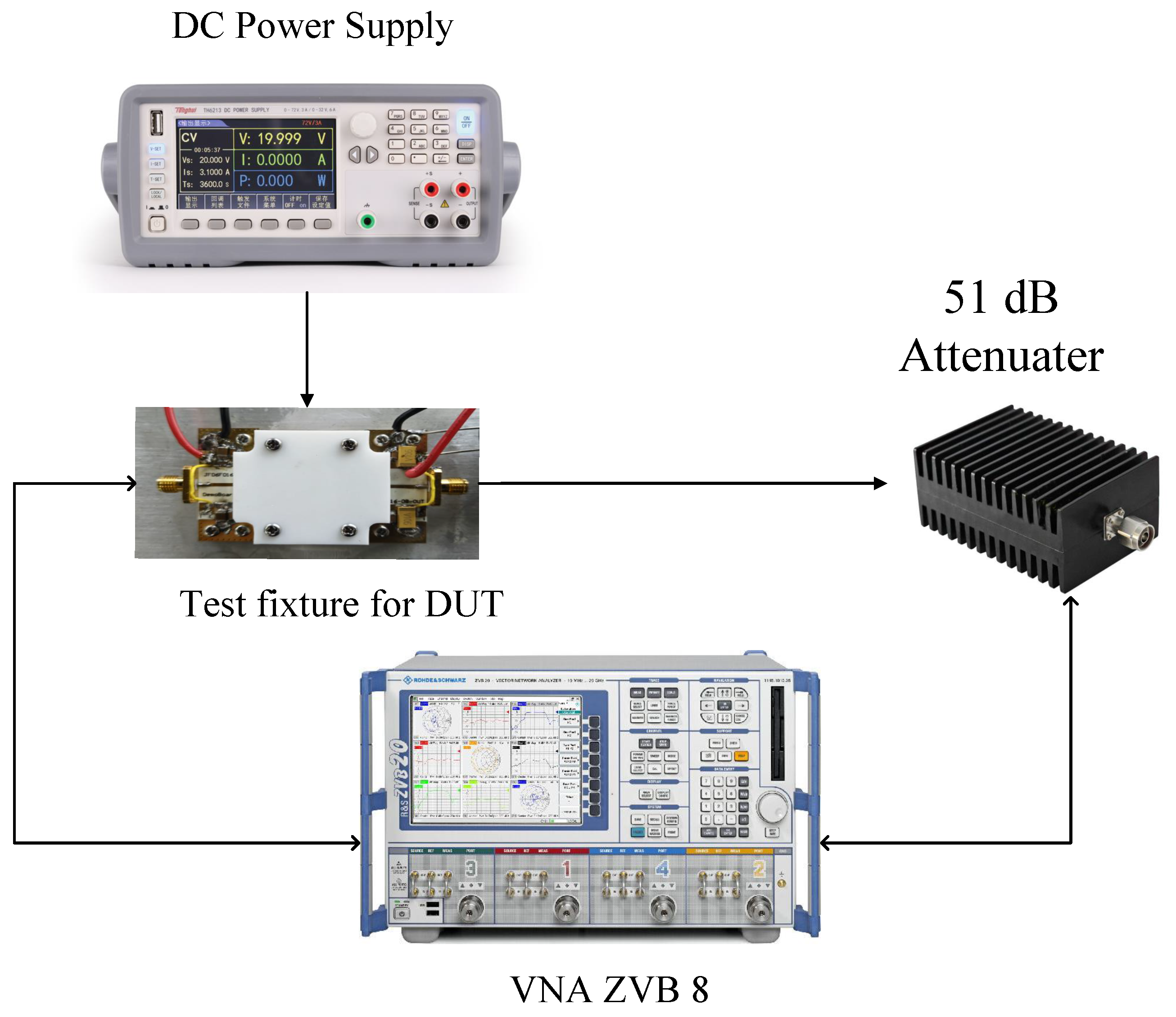
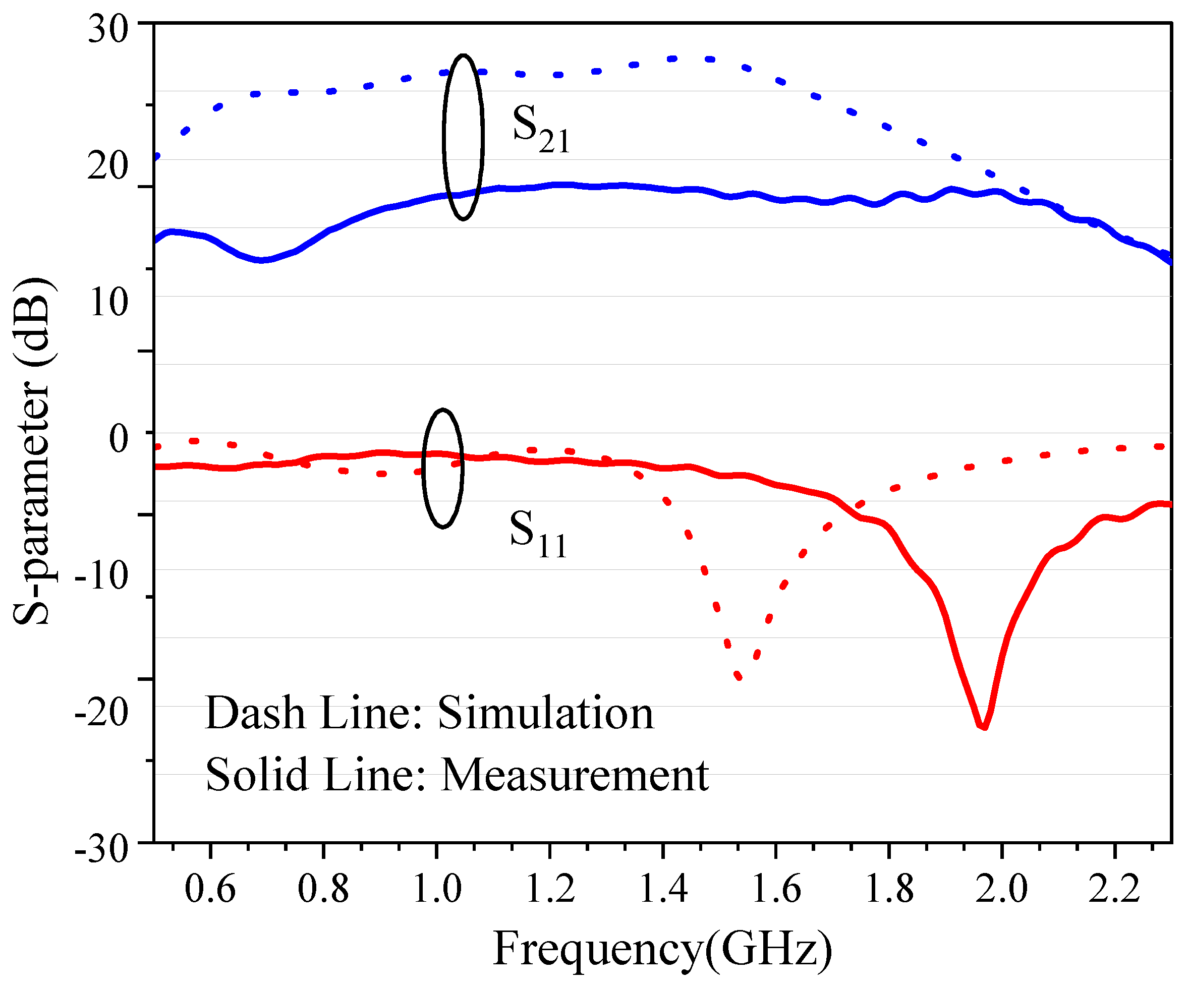
In order to figure out the small-signal performance of the designed PA, a test bed was used, which consists of Vector Network Analyzer ZVB 8 from Rohde and Schwarz, DC power supply, and 51 dB attenuator. The test bed setting is shown in Figure 13. The measured result is given in Figure 14. During the operation frequency, the proposed PA shows a stable small signal gain between 17 dB and 20 dB, which is lower than the simulation result. This may be caused by the accuracy of the GaN HEMT model, which will be further discussed in the next section.

3.2. Large Signal Test

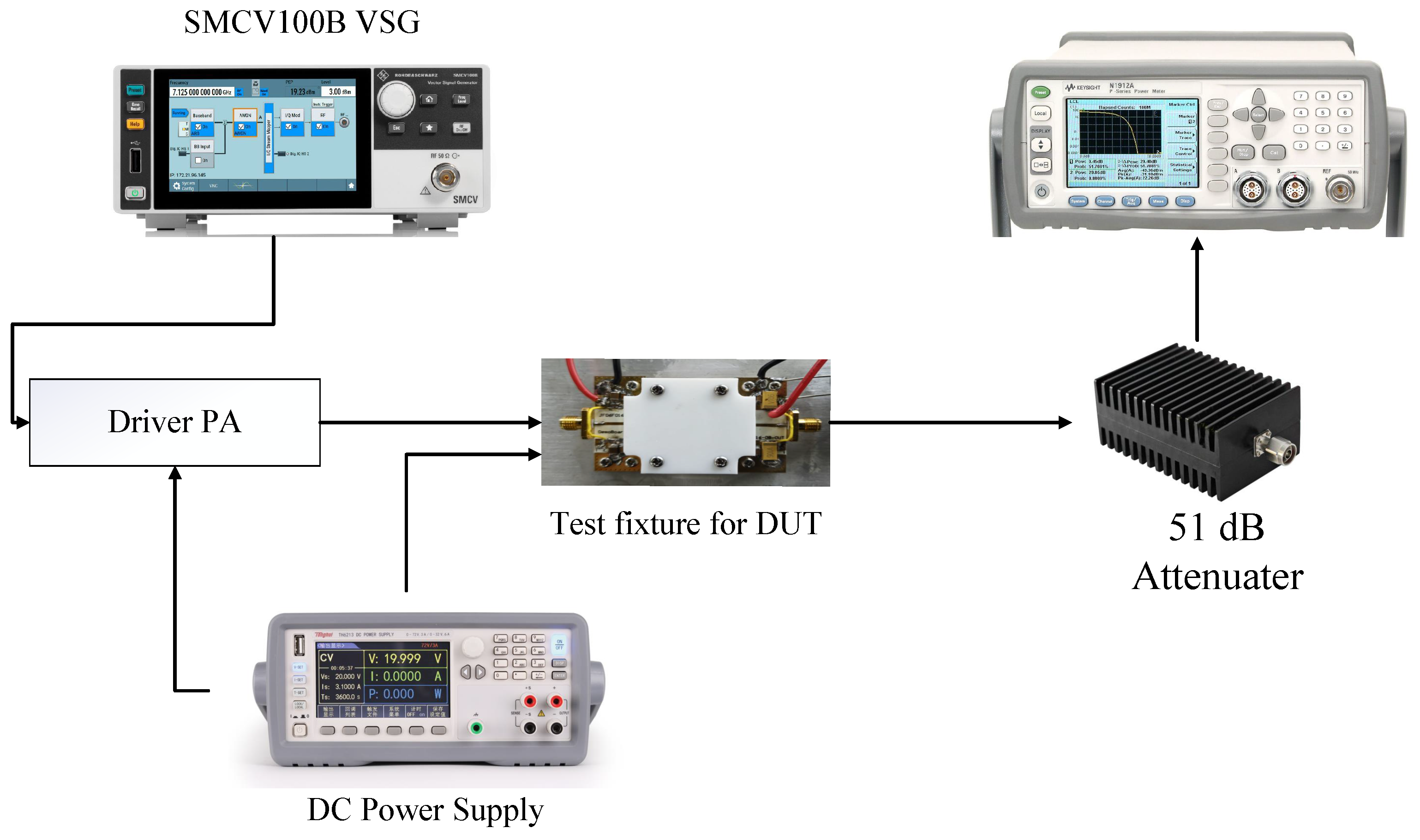
A large-signal test bed setting is shown in Figure 15. The signal generator is the SMCV100B Vector Signal Generator from Rohde and Schwarz. A driver amplifier before the DUT is applied to provide enough power stimulation. A Keysight N1912A Power Meter is employed to measure the accurate output power of the proposed PA. The DC voltage and current can be read from the DC power supply.
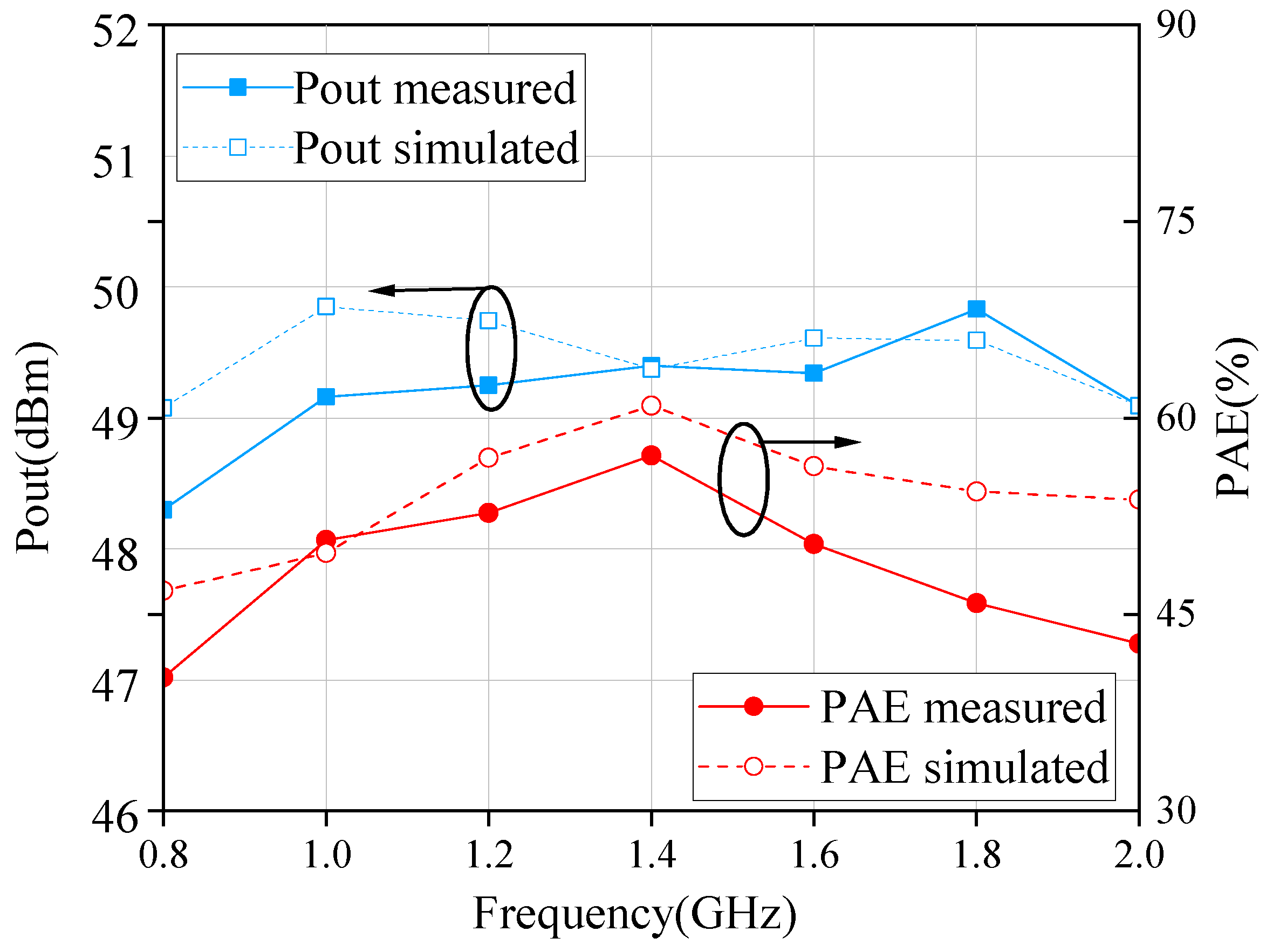
The drain voltage of the proposed amplifier is 50 V. The gate voltage is −0.235 V, and the test signal is a pulse signal with a duty cycle of 0.1. The output power and PAE results at different frequencies are shown in Figure 16. The minimum output power of the amplifier is 48.3 dBm at 0.8 GHz. The maximum output power is 49.83 dBm at 1.8 GHz. The output power is larger than 49 dBm except for 0.8 GHz. The minimum power additive efficiency is 40.18% at 0.8 GHz, and the maximum power additive efficiency is 57.1% at 1.4 GHz.
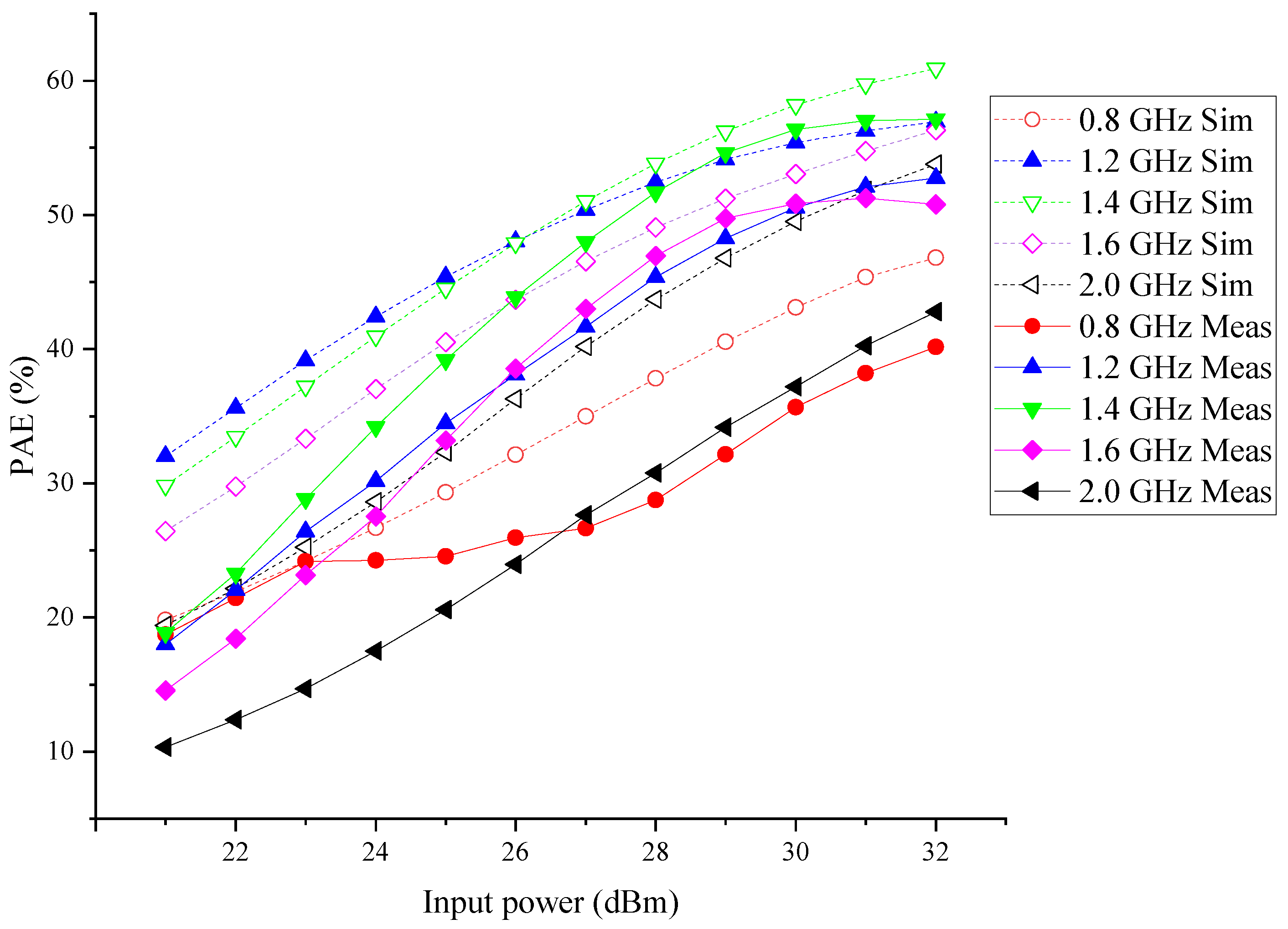
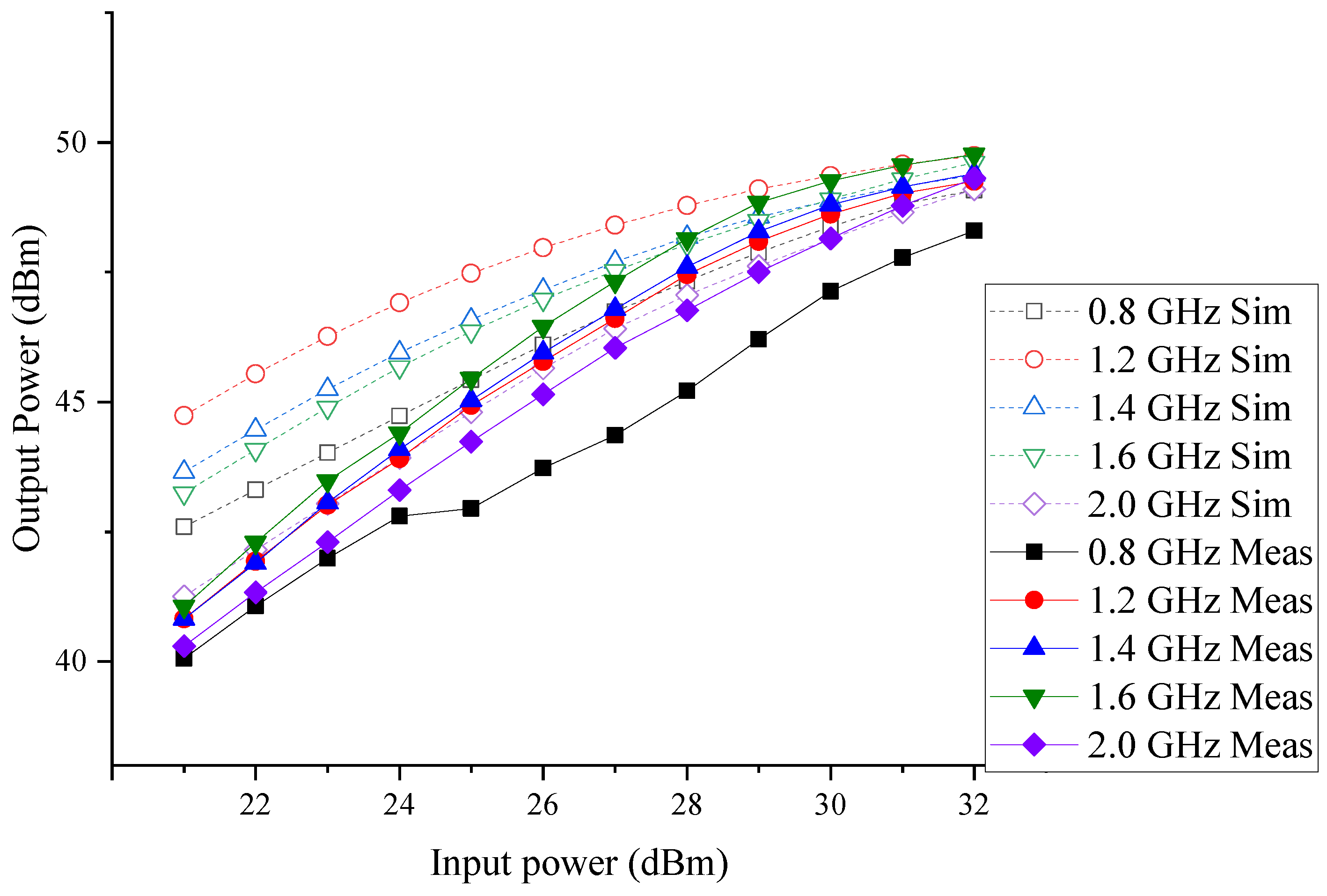
Figure 17 and Figure 18 show the power sweep measurement results and simulation results of the amplifier at 0.8 GHz, 1.2 GHz, 1.4 GHz, 1.6 GHz, and 2.0 GHz. The scanning input power is from 21 dBm to 32 dBm and the power step is 1 dB. It can be seen from Figure 17 and Figure 18 that the PAE and output power curves are close to the simulation shape at most frequencies. The performance degradation at the edges (0.8 GHz) of the frequency range is due to parasitic parameters of the circuit components. As given in Figure 17, the measured output power is lower than the simulation results. But when the PA comes close to saturation region, the power and simulation and measured result are more closed at most frequencies. This may caused by the accuracy of the GaN HEMT model, which may have less accuracy when the input power is lower. This can also be seen from the small-signal measurement results in Figure 14.
Table 1 summarizes the comparison of the research results of this paper with those of state-of-the-art research results obtained in recent years. We also use the power density factor ( P d = P o u t / c i r c u i t s i z e ) as a metric for comparing each PA. It can be seen that, compared with other published works, the PA proposed in this paper has close bandwidth but better gain and output power compared with similar work. Because of the implementation of the internally matched method, our circuit size is much smaller than these externally matched PAs.

4. Conclusions

For an electronic warfare system, the power, bandwidth, and circuit size of the power amplifier are very important. Traditional externally matched PAs can achieve wide bandwidth and high power but are difficult to have a small circuit size at the same time. In this paper, a GaN HEMT-based internally matched wide-band power amplifier is proposed. The proposed PA has an average output power of 49 dBm and operation frequency from 0.8 GHz to 2 GHz. The PAE during the whole operation bandwidth is from 40% to 57%. The internally matched structure can greatly reduce the circuit size compared with externally matched PAs, and the circuit size is 30.8 × 27.4 mm 2 . This circuit size is much smaller than similar state-of-the-art wide-band works. The high power, wide bandwidth, and compact circuit size make the proposed PA suitable for electronic warfare systems.

Author Contributions

Conceptualization, C.L.; methodology, C.L., Z.Z. and X.S.; validation, C.L., Y.P., C.C. and Z.Z.; writing—original draft preparation, C.L., Z.Z. and Y.L.; data curation, X.L.; writing—review and editing, C.L. and Y.X.; supervision, Y.X.; project administration, Y.X.; funding acquisition, Y.X. All authors have read and agreed to the published version of the manuscript.

Funding

This work is Supported by Sichuan Science and Technology Program under grant 192 No. 2024NSFJQ0022.

Data Availability Statement

The data that support the findings of this study are available within the article.

Conflicts of Interest

Author Yi Pei and Changchang Chen was employed by Dynax Semiconductor Inc. The remaining authors declare that the research was conducted in the absence of any commercial or financial relationships that could be construed as a potential conflict of interest.

References

  1. Spezio, A.E. Electronic warfare systems. IEEE Trans. Microw. Theory Tech. 2002, 50, 633–644. [Google Scholar] [CrossRef]
  2. Campbell, C.; Lee, C.; Williams, V.; Kao, M.Y.; Tserng, H.Q.; Saunier, P.; Balisteri, T. A Wideband Power Amplifier MMIC Utilizing GaN on SiC HEMT Technology. IEEE J. Solid-State Circuits 2009, 44, 2640–2647. [Google Scholar] [CrossRef]
  3. Yoshioka, T.; Harauchi, K.; Sugitani, T.; Maehara, H.; Yamasaki, T.; Ichinohe, H.; Miyashita, M.; Yamamoto, K.; Goto, S. Ku-Band 70-/30-W-Class Internally Matched GaN Power Amplifiers with Low IMD3 over a Wide Offset Frequency Range of up to 400 MHz. IEEE J. Solid-State Circuits 2021, 56, 2635–2646. [Google Scholar] [CrossRef]
  4. Jeong, J.; Pech, P.; Jeong, Y.; Lee, S. Wafer-Level-Packaged X -Band Internally Matched Power Amplifier Using Silicon Interposer Technology. IEEE Microw. Wirel. Compon. Lett. 2019, 29, 665–668. [Google Scholar] [CrossRef]
  5. Ayasli, Y.; Reynolds, L.D.; Mozzi, R.L.; Hanes, L.K. 2–20 GHz GaAs traveling-wave power amplifier. IEEE Trans. Microw. Theory Tech. 1984, 32, 290–295. [Google Scholar] [CrossRef]
  6. Hu, J.; Ma, K. A 0.1–52-GHz triple cascode amplifier with resistive feedback. IEEE Microw. Wirel. Compon. Lett. 2019, 29, 538–540. [Google Scholar] [CrossRef]
  7. Niclas, K.B. Multi-Octave Performance of Single-Ended Microwave Solid-State Amplifiers. IEEE Trans. Microw. Theory Tech. 2008, 32, 896–908. [Google Scholar] [CrossRef]
  8. Sayed, A.; Boeck, G. 5W highly linear GaN power amplifier with 3.4GHz bandwidth. In Proceedings of the 2007 European Microwave Conference, Munich, Germany, 9–12 October 2007; pp. 1429–1432. [Google Scholar]
  9. Le, Q.H.; Zimmer, G. Wideband High Efficiency 50 W GaN-HEMT Balanced Power Amplifier. In Proceedings of the 2018 48th European Microwave Conference (EuMC), Madrid, Spain, 23–27 September 2018; pp. 348–351. [Google Scholar]
  10. Srinidhi, E.R.; Masood, M.; Sharma, T.; Staudinger, J.; Dhar, S.K.; Rashev, P.; Tucker, G.; Ghannouchi, F.M. Digitally Assisted Load Modulated Balanced Amplifier for 200W Cellular Infrastructure Applications. In Proceedings of the 2020 IEEE/MTT-S International Microwave Symposium (IMS), Los Angeles, CA, USA, 4–6 August 2020; pp. 719–722. [Google Scholar]
  11. Samis, S.; Friesicke, C.; Maier, T.; Quay, R.; Jacob, A.F. A 41.5 dBm Broadband AlGaN/GaN HEMT Balanced Power Amplifier at K-Band. In Proceedings of the 2021 16th European Microwave Integrated Circuits Conference (EuMIC), London, UK, 3–4 April 2022; pp. 164–167. [Google Scholar]
  12. Chen, K.; Peroulis, D. Design of highly efficient broadband classE power amplifier using synthesized low-pass matching networks. IEEE Trans. Microw. Theory Tech. 2011, 59, 3162–3173. [Google Scholar] [CrossRef]
  13. Zheng, S.Y.; Liu, Z.W.; Zhang, X.Y.; Zhou, X.Y.; Chan, W.S. Design of Ultrawideband High-Efficiency Extended Continuous Class-F Power Amplifier. IEEE Trans. Ind. Electron. 2018, 65, 4661–4669. [Google Scholar] [CrossRef]
  14. Yang, M.; Xia, J.; Guo, Y.; Zhu, A. Highly Efficient Broadband Continuous Inverse Class-F Power Amplifier Design Using Modified Elliptic Low-Pass Filtering Matching Network. IEEE Trans. Microw. Theory Tech. 2016, 64, 1515–1525. [Google Scholar] [CrossRef]
  15. Trenz, F.; Hofmann, M.; Weigel, R.; Fischer, G.; Kissinger, D. Compact 2–28 GHz planar multi-octave bandwidth Wilkinson power dividers. In Proceedings of the 2014 IEEE MTT-S International Microwave Symposium (IMS2014), Tampa, FL, USA, 1–6 June 2014; pp. 1–4. [Google Scholar]
  16. Chi, P.-L.; Yang, T. A 1.3–2.08 GHz Filtering Power Divider with Bandwidth Control and High In-Band Isolation. IEEE Microw. Wirel. Compon. Lett. 2016, 26, 407–409. [Google Scholar] [CrossRef]
  17. Zhang, Z.; Arnous, M.T.; Boeck, G. Ultra-broadband GaN power amplifier utilizing planar Guanella transformer. In Proceedings of the 2015 17th International Conference on Transparent Optical Networks (ICTON), Budapest, Hungary, 5–9 July 2015; pp. 1–4. [Google Scholar]
  18. Arnous, M.T.; Zhang, Z.; Barbin, S.E.; Boeck, G. A novel design approach for highly efficient multioctave bandwidth GaN power amplifiers. IEEE Microw. Wirel. Compon. Lett. 2017, 27, 371–373. [Google Scholar] [CrossRef]
  19. Zhang, Z.; Cheng, Z.; Ke, H.; Liu, G.; Li, S. Design of a broadband high-efficiency hybrid class-EFJ power amplifier. IEEE Microw. Wirel. Compon. Lett. 2020, 30, 407–409. [Google Scholar] [CrossRef]
  20. Bidgoli, H.A.; Khodaei, M.; Tayarani, M. Multioctave Power Amplifier Design Using 9:1 Planar Impedance Transformer. IEEE Microw. Wirel. Compon. Lett. 2021, 31, 45–48. [Google Scholar] [CrossRef]
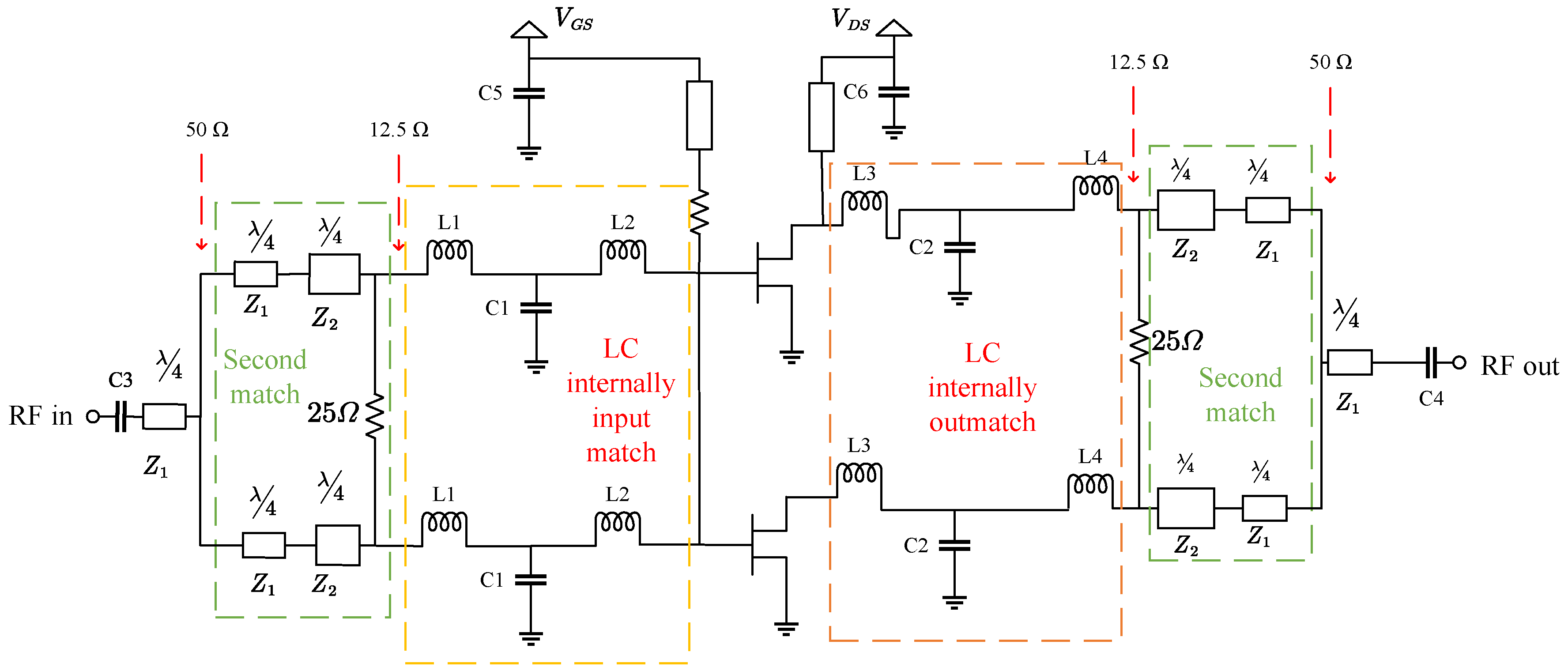
Figure 1. Schematic diagram of the proposed PA.
Electronics 13 02687 g001
Figure 2. Best PAE impedance in load-pull simulation results from 0.8 GHz to 2.0 GHz; PAE in red zone is larger than 75 % at 1.4 GHz; the pentagram is the chosen impedance.
Electronics 13 02687 g002
Figure 3. The schematic diagram of the input matching network and layout of the LC input matching network.
Electronics 13 02687 g003
Figure 4. S-parameter simulation result of input match network.
Electronics 13 02687 g004
Figure 5. Schematic diagram of the output matching network and layout of the LC matching network.
Electronics 13 02687 g005
Figure 6. The simulation result of the output matching network.
Electronics 13 02687 g006
Figure 7. Schematic diagram of gold-bonding-wire-spiral inductor composite structure, where green part is substrate, yellow part is micro-strip line and bonding wire.
Electronics 13 02687 g007
Figure 8. Equivalent circuit model of gold-bonding-wire-spiral inductor composite structure.
Electronics 13 02687 g008
Figure 9. Schematic diagram of two-stage power divider.
Electronics 13 02687 g009
Figure 10. Schematic diagram and layout of power divider in proposed PA design.
Electronics 13 02687 g010
Figure 11. The S-parameter simulation result of the power divider/combiner.
Electronics 13 02687 g011
Figure 12. Photo of the proposed internally matched PA.
Electronics 13 02687 g012
Figure 13. The small-signal measurement test bed setting.
Electronics 13 02687 g013
Figure 14. The small-signal measurement result and simulation result.
Electronics 13 02687 g014
Figure 15. A large-signal measurement test bed setting.
Electronics 13 02687 g015
Figure 16. Large signal measurement with different frequencies (input power: 32 dBm).
Electronics 13 02687 g016
Figure 17. PAE result with different input power and frequencies.
Electronics 13 02687 g017
Figure 18. Output Power result with different input power and frequencies.
Electronics 13 02687 g018
Table 1. Comparison of state-of-the-art PA.
ReferenceFreq (GHz)Pout (dBm)Gain (dB)PAE (%)Size P d
2015 [17]0.4–2.842–43.7945NANA
2017 [18]0.5–2.743–45.48–10.456–70 110 × 50 mm 2 0.6304
2018 [13]0.5–2.339.2–41.211.7–25.352.7–80.7 95 × 57 mm 2 0.2434
2020 [19]1.2–3.639.59–43.110–1457.6–67.2NANA
2021 [20]0.5–3.046–47.510–11.550–60 92 × 40 mm 2 1.5281
This work0.8–248.3–49.816.3–17.840.17–57.1 30.8 × 27.4 mm 2 11.3162
Disclaimer/Publisher’s Note: The statements, opinions and data contained in all publications are solely those of the individual author(s) and contributor(s) and not of MDPI and/or the editor(s). MDPI and/or the editor(s) disclaim responsibility for any injury to people or property resulting from any ideas, methods, instructions or products referred to in the content.