Article

A 2.0–3.0 GHz GaN HEMT-Based High-Efficiency Rectifier Using Class-EFJ Operating Mode

1
School of Electronics and Information, Hangzhou Dianzi University, Hangzhou 310005, China
2
ECIT Institute, Queen’s University Belfast, Belfast BT7 1NN, UK
*
Author to whom correspondence should be addressed.
Electronics 2024, 13(14), 2786; https://doi.org/10.3390/electronics13142786 (registering DOI)
Submission received: 25 May 2024 / Revised: 4 July 2024 / Accepted: 15 July 2024 / Published: 16 July 2024

Abstract

:
In this paper, a CGH40010F GaN-based wideband RF rectifier with high rectification efficiency is presented. A novel continuous class-EFJ-mode rectifier is constructed by combining a continuous class-J-mode rectifier and class-EF-mode rectifier under specific impedance conditions. This novel continuous class-EFJ-mode rectifier has high rectification efficiency and wide bandwidth at the same time. For validation, a wideband high-efficiency class-EFJ-mode rectifier functioning within the 2.0–3.0 GHz range is designed, fabricated, and measured. The measurements indicate that, with an input power of 40 dBm and a resistance of 72 Ω on the dc load, the implemented rectifier sustains a rectification efficiency exceeding 60% across its entire operational frequency band. Meanwhile, the dimensions of the circuits are only 3 cm × 3.1 cm.

1. Introduction

Recently, the scenario that can provide a high-capacity wireless power supply for vehicles and drones has gradually attracted much attention with the development of wireless power transmission technologies [1]. In the context of a wireless energy transmission system, the radio frequency (RF)-DC rectifier stands as a pivotal circuit module, and its performance is absolutely critical to the efficient operation of the entire system [2]. In order to obtain the optimum energy density and efficiency of the wireless power transmission, the rectifier needs to maintain high efficiency across a wide frequency band [3]. Conventional diode-based rectifiers have realized wide-bandwidth and high-efficiency operation [4,5,6,7]. In [4], a BAT15-03W Schottky diode-based broadband rectifier with a rectification efficiency of over 70% is implemented in the frequency band from 1.77 GHz to 2.85 GHz at the input power level of 11.5-dBm. In [5], an ultra-wideband high-efficiency rectifier is designed with an input power capacity of 23 dBm using a diode MAE1347B. In [6,7], a broadband radio frequency (RF) energy harvester is presented using a Schottky HSMS-2862 diode, which can work efficiently in a wide frequency band. The state-of-the-art performance of diode-based rectifiers is listed in Table 1. Table 1 indicates that the power capacity of diode-based rectifiers is typically less than 1 W. Although diode-based rectifiers can achieve good bandwidth and rectification efficiency, diode-based rectifiers’ power capacity is low, which fails to satisfy the requirements of application situations with high performance capacity (at least 10 W).
In order to meet the requirements of high-power-capacity applications, transistor-based rectifiers have recently become promising solutions due to their high power capacity. Using the concept of the time-reversal duality, transistor-based rectifiers are evolved from the original power amplifiers [13]. Several transistor-based rectifiers with high efficiency, such as class-F [14], class-F−1 [15], and our recent work, class-GF [16], have been investigated. However, these rectifiers are narrowband, while high-efficiency transistor-based rectifiers with wide bandwidth are rarely reported. Most of the existing bandwidth enhancement methods for transistor-based rectifiers are achieved by the introduction of broadband phase shift networks [17,18]. The theoretical studies on the operation modes of rectifiers with wide bandwidth and high efficiency are inadequate.
Therefore, different from the presented technology, this paper investigates the operation mode of the rectifier itself. Through the analysis of the impedance characteristics of conventional class-EF rectifiers and continuous class-J rectifiers, it is found that class-EF rectifiers and continuous class-J rectifiers can be effectively merged under certain conditions. As a result, a rectifier called continuous class-EFJ-mode is constructed, which incorporates the high-efficiency characteristics of the class-EF with the broadband characteristics of the continuous class-J mode. The load impedance of the novel class-EFJ rectifier is theoretically derived. The introduction of the continuous-mode parameter has resulted in the fundamental and second-harmonic impedances of the continuous class-EFJ rectifier becoming a dynamic range rather than a fixed value. This extended impedance space provides convenience for the design of the broadband matching network. This flexibility is advantageous in widening the operating bandwidth of the rectifier. To substantiate the efficacy of the proposed approach, a continuous class-EFJ rectifier utilizing a GaN HEMT is designed and fabricated.

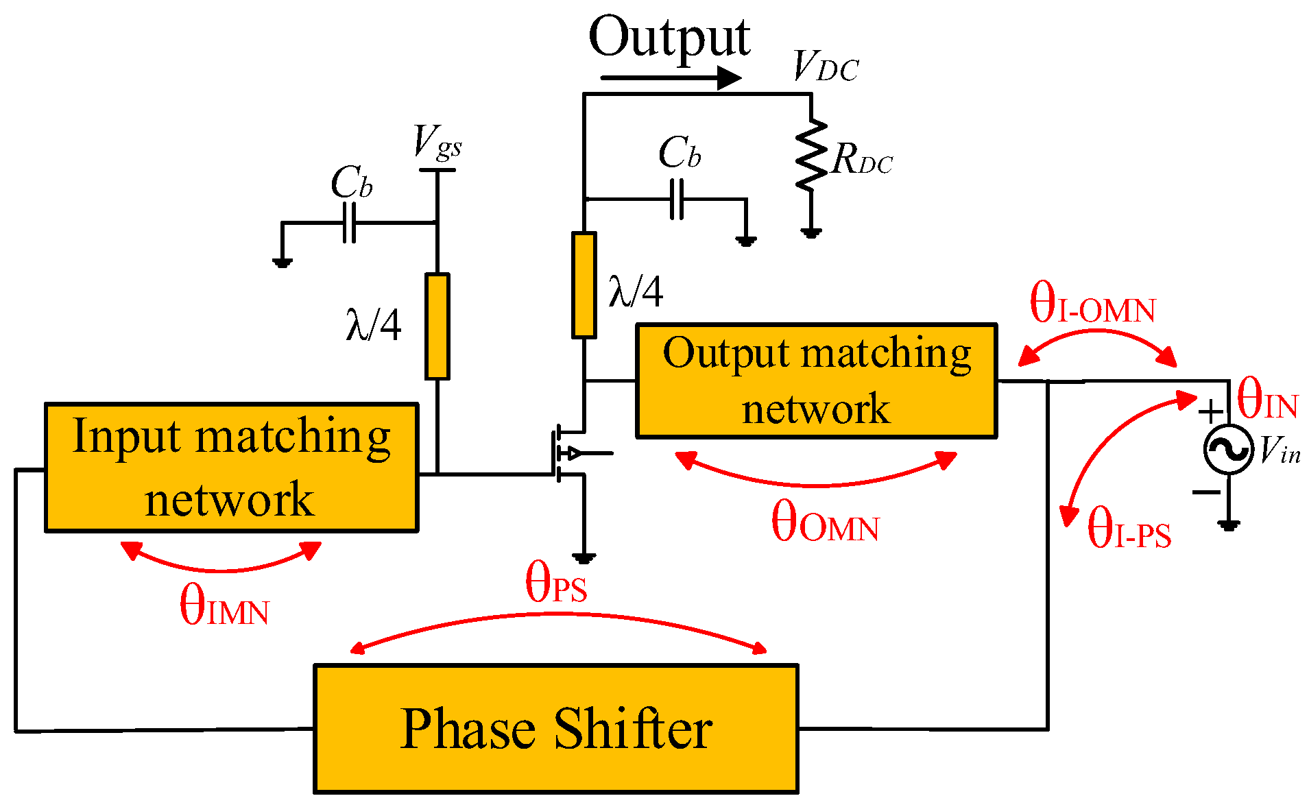
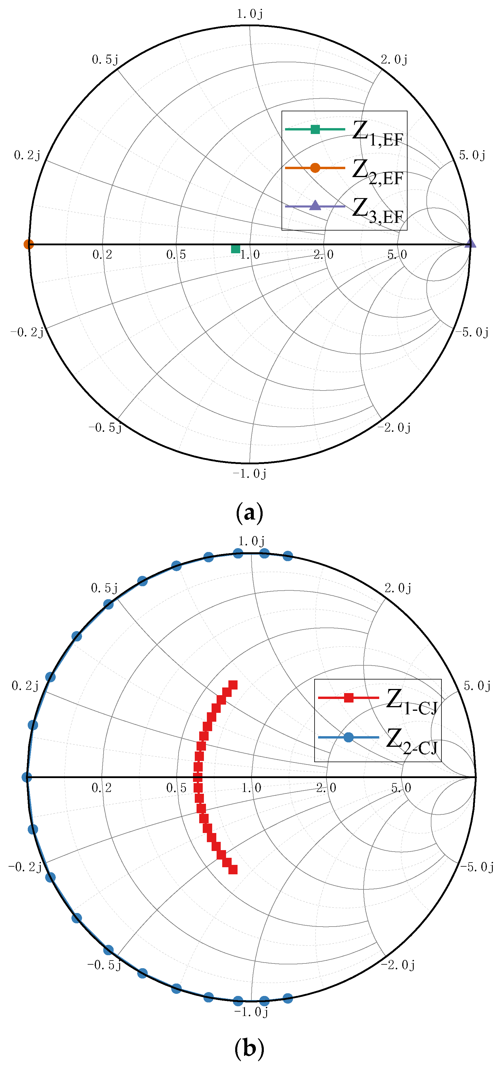
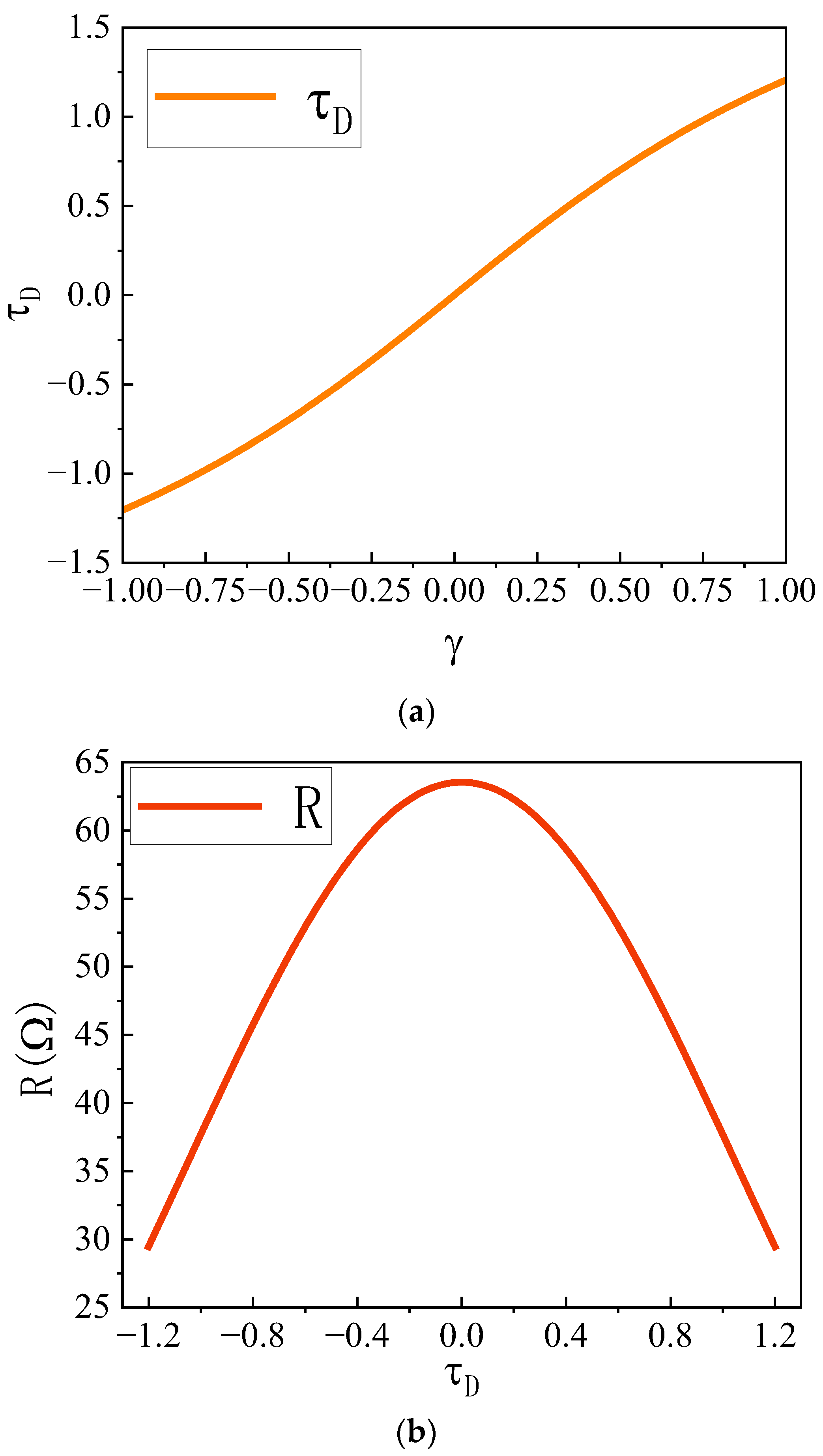
2. Analysis of the Proposed Rectifier

Figure 1 presents the GaN HEMT-based rectifier topology, which is converted from a power amplifier according to the principle of the time-reversal duality [19]. In the architecture of the transistor-based rectifier, the RF output terminal and DC drain bias of the original power amplifier are used as the RF input terminal and DC output terminal of the rectifier, respectively. As illustrated in Figure 1, the rectifier mainly consists of four parts: the input matching network (with a phase θIMN), the output matching network (with a phase θOMN), the gate bias line and the phase shift network, and θPS is the phase shift imparted by the phase shifter network. θIN represents the phase of the input power, θI-OMN is the phase shift from the input to output matching network, and θI-PS refers to the phase shift from the input to phase shift network.
Utilizing the principle of time-reversal duality, the designed rectifier can be achieved via the conversion of the power amplifier. Therefore, using the conventional class-EF-mode PA described in [20] as a reference, the corresponding fundamental and harmonic load impedance, Z1,EF, Z2,EF, and Z3,EF, of the conventional class-EF-mode rectifier are delineated as follows.
Z 1 , E F = ( 1 + j     A ) R  
A = τ D 0.5 s i n 2 τ D s i n τ D s i n τ D , R = 2 1 + cos τ D 2 π 2 V D C 2 P o
Z 2 , E F = 0 Z 3 , E F =    
where τD denotes the turn-off time of the transistor (in radians). Po denotes the output power, and VDC represents the dc bias voltage. Based on (1)–(3), Figure 2a plots the load impedance space of the class-EF mode. The load impedance of the EF mode is limited to a fixed value. Although it can achieve high efficiency through the switch operation harmonious control, it is obvious that its working bandwidth is very narrow.
Accordingly, drawing upon the theory of the continuous class-J-mode PA in [21], the corresponding fundamental load impedance Z1-CJ and second-harmonic load impedances Z2-CJ of the continuous class-J-mode rectifier are formulated as
Z 1 C J = 1 + j γ R o p t
Z 2 C J = j 3 π γ 8 R o p t  
where γ represents the continuous-mode parameter, the value of which falls within the range of −1 and 1. Additionally, Ropt signifies the optimal load impedance for the device being utilized, computable as follows:
R o p t = 2 V D C V K I m a x
where VK is the knee voltage of the transistor. Imax signifies the maximum current. Based on (4)–(6), Figure 2b shows the load impedance space of the continuous class-J mode. It can be observed from the figure that, compared with the class-EF mode, due to the introduction of continuous-mode parameter γ, the impedance space of the J mode has expanded. This extended impedance space can be used to achieve large bandwidth. However, the expansion of impedance is exchanged at the cost of reducing efficiency. Therefore, compared with the EF mode’s ideal 100% efficiency, the efficiency of continuous J mode can usually only reach about 78.5%.
Based on the above descriptions of the EF mode and continuous J mode, it can be concluded that they have their own advantages and deficiencies; that is, the EF mode has high efficiency but narrow bandwidth, and the continuous J mode has a wide bandwidth but low efficiency. Therefore, how to combine the advantages of the two to realize a working model with both bandwidth and high efficiency is worth further exploring.
Next, by analyzing the impedance expression of the two modes, we look for the possibility of integrating the two modes. Upon comparing (1) with (4), it becomes apparent that the load impedance formulations for class-EF and continuous class-J bear similarities. To facilitate the integration of these two operational modes, the following relationships need to be met:
( 1 + j γ ) R o p t = ( 1 + j A ) R A = γ R = R o p t
By utilizing (2) and (7), the τD can be determined to fall within the range of −1.20601 to 1.20601, provided that γ remains between −1 and 1. The correlation between τD and γ is graphically represented in Figure 3a.
This paper utilizes the Cree CGH40010F as the primary active device. Given that VK is approximately 5 V, VDC is set as 28 V, and Imax stands at 1.5 A. Then, the optimum load Ropt can be determined using (6) and is calculated to be 30.7 Ω. Furthermore, (2) can be used to calculate the value of R, provided that the condition of −1.20601 ≤ τD ≤ 1.20601, Po = 10 W, VDC = 28 V. Figure 3b illustrates the value of R versus τD. As depicted in Figure 3b, the value of R ranges from 29.24 Ω to 63.55 Ω. Evidently, the value of Ropt falls within this range, thus confirming the validity of (7). It is indicated that the class-EF-mode rectifier and the continuous class-J-mode rectifier can be combined when certain impedance conditions are satisfied. Then, the fundamental and harmonic load impedances of the continuous class-EFJ-mode rectifier can be expressed as
Z 1 E F J = ( 1 + j γ ) R  
Z 2 E F J = j 3 π γ 8 R ,   Z 3 E F J =
where R is between 29.24 Ω and 63.55 Ω.
The load impedances of the proposed continuous class-EFJ-mode rectifier expressed in (8) and (9) are illustrated in Figure 4. From Figure 4, it is evident that, when γ = 0, the fundamental load impedance of the continuous class-EFJ-mode-rectifier conforms to the expression of the fundamental load impedance of the traditional class-EF-mode rectifier. Additionally, the conditions for a shortened circuit at the second harmonic and an open circuit at the third harmonic are satisfied. When γ assumes other values, the class-EFJ-mode rectifier operates as the continuous class-J-mode rectifier, leading to expanded impedance ranges as parameter γ varies. Further, in comparison to the traditional continuous class-J, the introduction of the additional variable parameter R offers an expanded resistive impedance space. This broadened impedance design space subsequently enables a wider operational bandwidth.

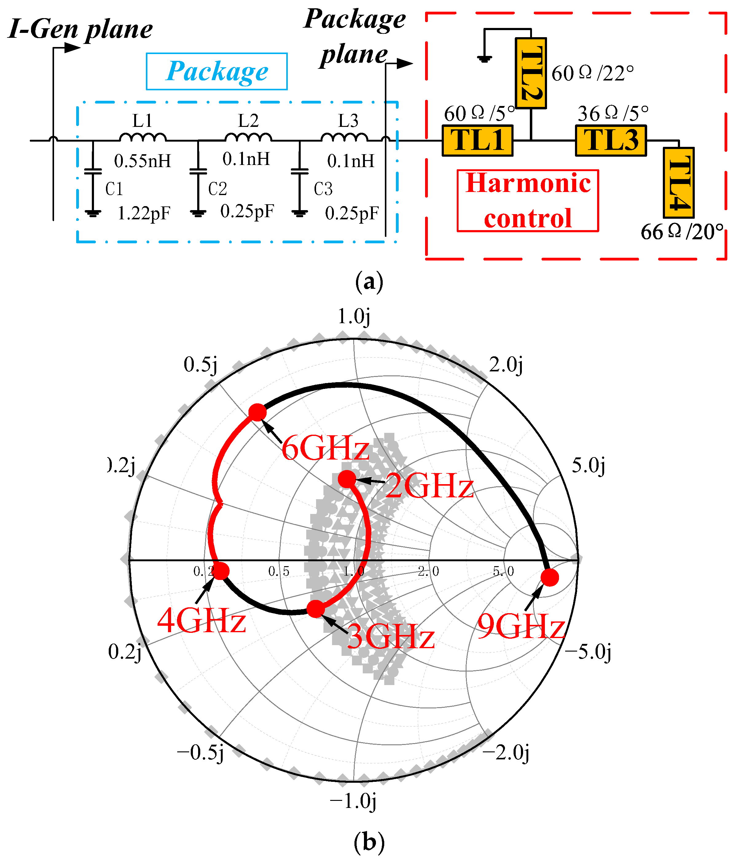
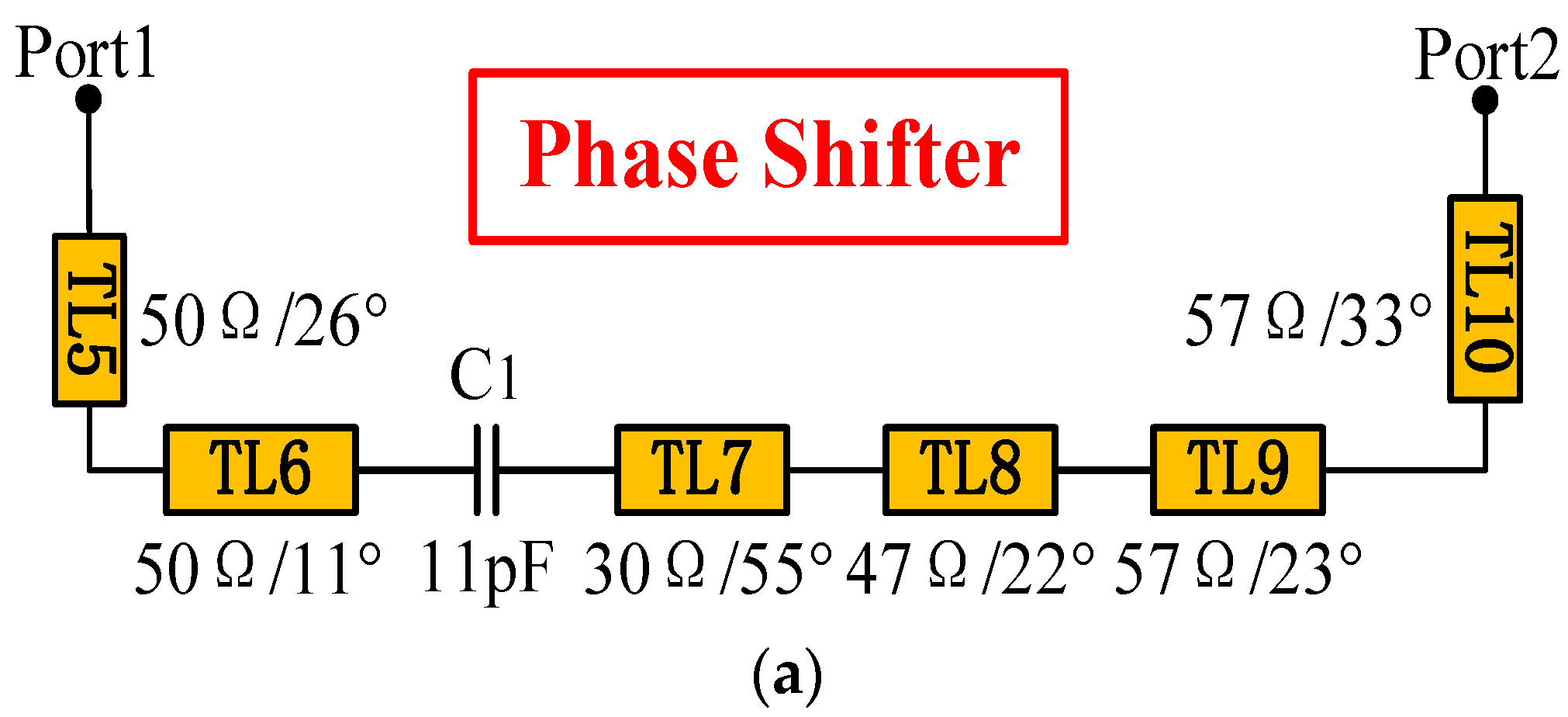
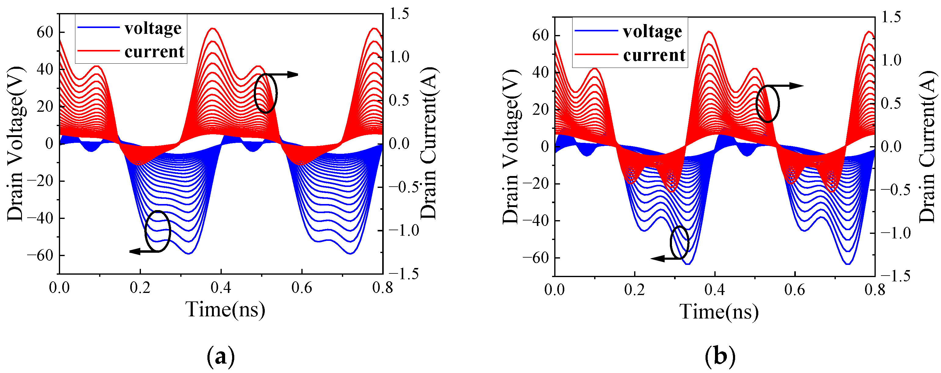
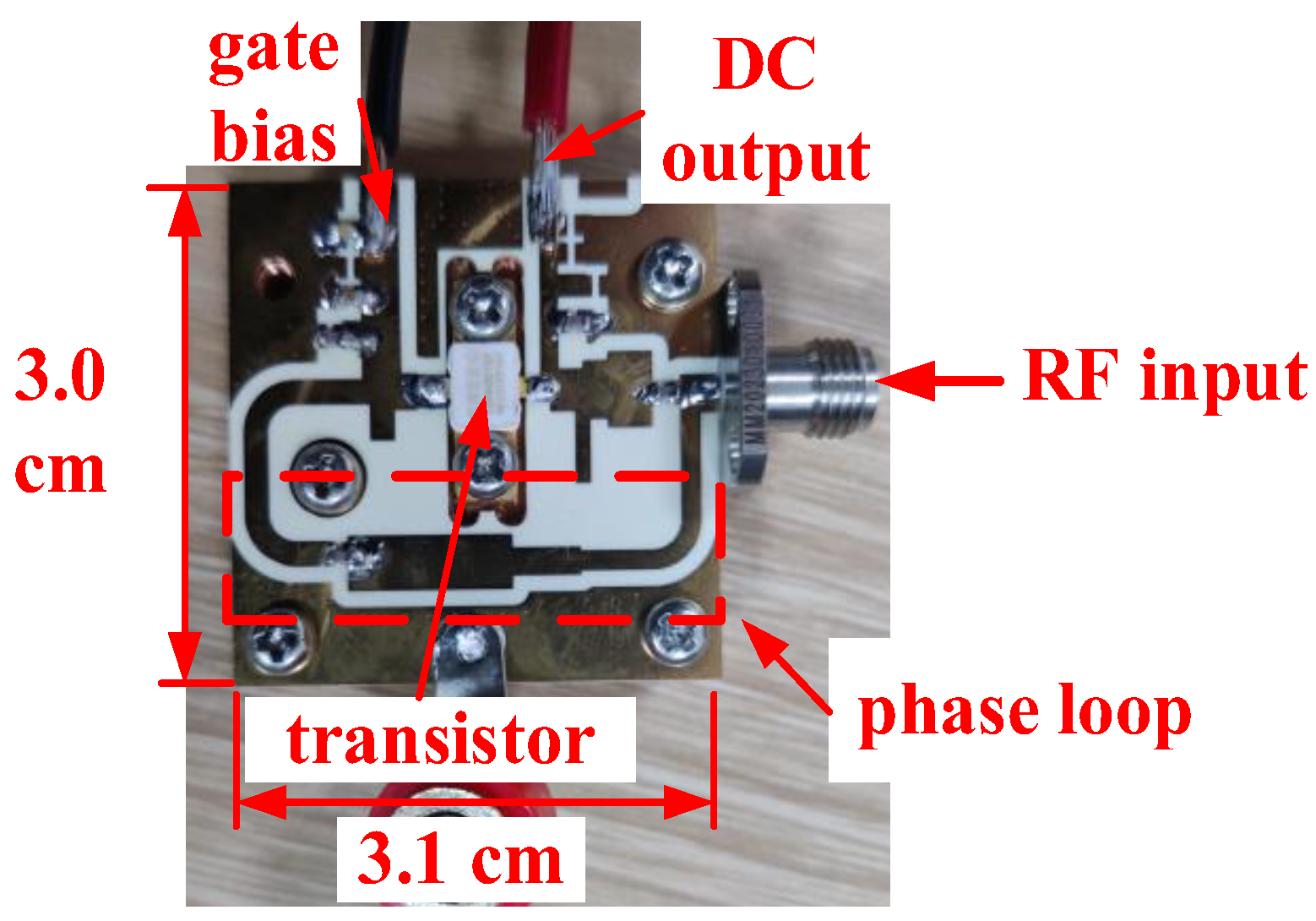
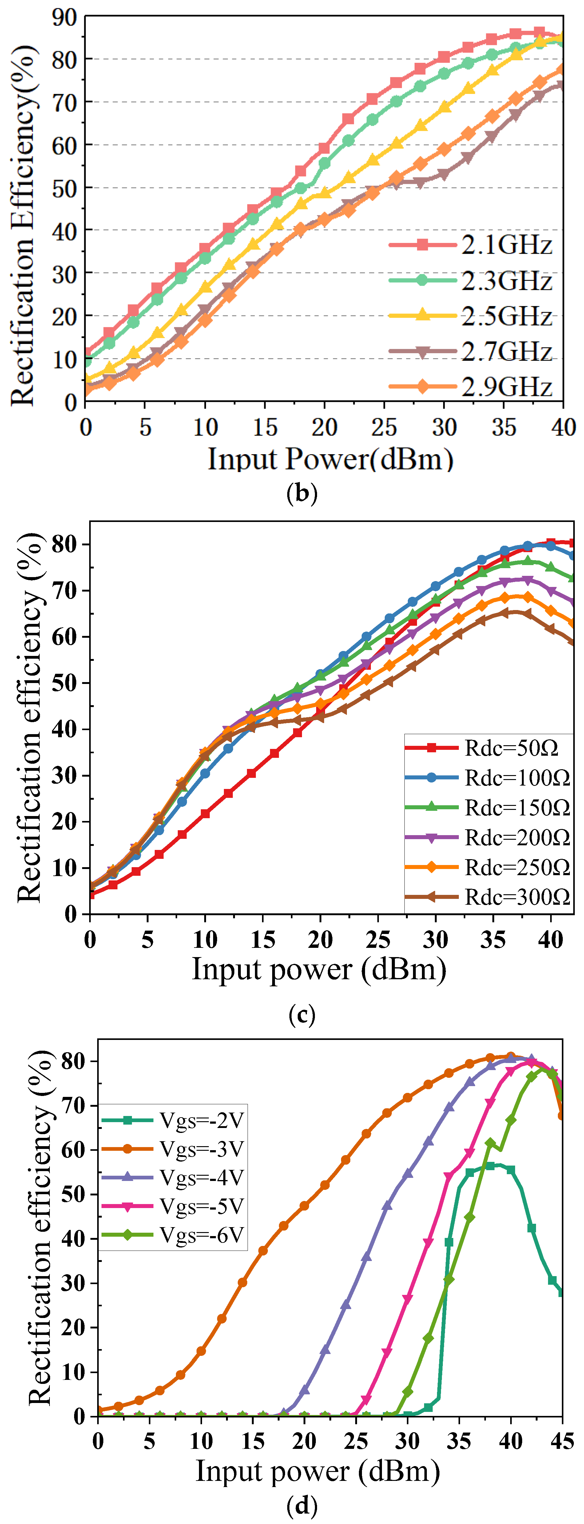
3. Design of the Rectifier

For validation, a wideband high-efficiency class-EFJ-mode rectifier operational within the 2.0–3.0 GHz frequency range is designed based on Rogers 4350B substrate (εr = 3.66, h = 30 mil) using a CGH40010F GaN HEMT, which is modeled in [22].
The gate voltage Vgs is set to −3.2 V based on the previously derived τD. Ropt is taken as 30.7 Ω. For the continuous class-EFJ-mode rectifier, the theoretical second-harmonic impedance is purely reactive, and the theoretical third-harmonic impedance approaches infinity. The designed harmonic control network, depicted in Figure 5a, employs transmission lines TL1 and TL2 to meet the second-harmonic impedance requirements. Transmission lines TL1, TL3, and TL4 are used to satisfy the third-harmonic impedances expressed in (9). The output matching network is designed in 2.0–3.0 GHz using the stepped impedance matching technology. The package parameters of this device are integrated into the output network after undergoing minor optimization in ADS 2022 software. The simulated impedance at the output is shown in Figure 5b. It is observable that the load impedance lies within the theoretical impedance space, as expressed in (8) and (9).
The necessary phase disparity between the gate and the drain (θDG) terminals is 180° or an odd multiple of 180° according to [15]. As shown in Figure 1, the phase difference is expressed as
θ D G = ( θ I O M N + θ O M N ) (   θ I P S + θ P S + θ I M N ) = ( 2 n + 1 ) π   ( r a d )  
A wideband phase-shift network needs to be designed to satisfy the desired phase difference θDG. As shown in Figure 6a, transmission lines TL5–TL10 are employed to realize the desired phase conversion. The phase θDG between the gate and drain nodes and the phase θPS of the shift network are illustrated in Figure 6b. As depicted in Figure 6b, the θPS values exhibit a range of −157.8° to −177.6° within the frequency band of 2.0–2.4 GHz, whereas they span from 179.9° to 151.8° within 2.45–3.0 GHz. The value of θDG is between 180.5° and 184.7° in 2.0–3.0 GHz, which is approximately equal to 180° defined in (10). Meanwhile, the stepped impedance matching technology is utilized to match the source impedance to the standard terminal impedance. Then, the phase shift network and the input and output networks are combined into a completed rectifier circuit that is shown in Figure 7.
The waveforms for voltage and current at the drain are simulated with RF input power levels ranging from 20 to 40 dBm. The simulated waveforms are shown in Figure 8, in which the voltage (blue) is negative and the current (red) is positive. As presented in [23], transistor-based rectifiers have positive and negative operating polarities. The class-EFJ-mode rectifier, designed as such, depicts a negative polarity in operation. A photograph depicting the fabricated rectifier, measuring 3 cm × 3.1 cm in size, is presented in Figure 9.
Testing has been conducted on the fabricated rectifier, and the measurements are presented in Figure 10a. With an RF input power at 40 dBm and a dc load at 72 Ω, the measured rectification efficiency of the rectifier ranges from 60% to 87% across the 2.0–3.0 GHz range. In particular, as shown in Figure 8b, at 2.7 GHz, the voltage and current have more overlapping portions, which increases the losses. This leads to a significantly lower efficiency than that of other frequencies. Figure 10b shows the dynamic profiles of rectification efficiency versus RF input power at several representative frequencies. With an increase in the RF input power ranging from 20 dBm to 40 dBm, the rectification efficiency experiences a significant rise from 40% to 85%. Figure 10c,d illustrate the rectification efficiency profiles for different RF input power levels under varying conditions at 2.45 GHz, including the gate bias voltages (Vgs) and DC loads (Rdc). Furthermore, as shown in Figure 10b,c, the rectification efficiency profiles exhibit distinct patterns due to changes in the dc load and gate bias voltages.
Table 2 presents some of the relevant rectifier works. As shown in Table 1, the class-EFJ-mode rectifier presented exhibits excellent operating bandwidth and rectification efficiency among GaN HEMT-based broadband rectifiers. Meanwhile, the proposed rectifier boasts a greater input power capability when compared to rectifiers that utilize diodes.

4. Conclusions

This paper proposes a high-efficiency GaN-based wideband RF rectifier. The integration of the class-EF rectifier mode and the continuous class-J rectifier mode serves to notably broaden the operating bandwidth of the class-EFJ rectifier. For validation, a continuous class-EFJ rectifier is fabricated, operable within the frequency range of 2.0–3.0 GHz. The rectification efficiency ranging from 60% to 87% can be realized over the entire operating frequency band when the input power is set to 40 dBm and the DC load is 72 Ω. In comparison to the related rectifiers, the class-EFJ rectifier implemented in this paper demonstrates strong competitiveness in terms of both efficiency and bandwidth.

Author Contributions

Conceptualization, C.W., J.L. and H.Z.; methodology, C.W. and J.L.; software, C.W., J.L. and H.Z.; validation, C.W., J.L. and L.Z.; formal analysis, C.W., J.L. and H.Z.; investigation, H.Z. and L.Z.; resources, C.W., J.L. and H.Z.; data curation, C.W., J.L. and H.Z.; writing—original draft preparation, C.W. and J.L.; writing—review and editing, C.W., J.L. and H.Z.; visualization, C.W., J.L. and L.Z.; supervision, Z.Z. and C.G.; project administration, Z.Z.; funding acquisition, Z.Z. and C.G All authors have read and agreed to the published version of the manuscript.

Funding

This work was funded by the National Natural Science Foundation (Grant 62201181).

Data Availability Statement

Data are contained within the article.

Conflicts of Interest

The authors declare no conflicts of interest.

References

  1. Akan, O.B.; Cetinkaya, O.; Koca, C.; Ozger, M. Internet of Hybrid Energy Harvesting Things. IEEE Internet Things J. 2018, 5, 736–746. [Google Scholar] [CrossRef]
  2. Niyato, D.; Kim, D.I.; Maso, M.; Han, Z. Wireless powered communication networks: Research directions and technological approaches. IEEE Wirel. Commun. 2017, 24, 88–97. [Google Scholar] [CrossRef]
  3. Nguyen, D.M.; Au, N.D.; Seo, C. A microwave power transmission system using sequential phase ring antenna and inverted class F rectenna. IEEE Access 2021, 9, 134163–134173. [Google Scholar] [CrossRef]
  4. Bui, G.T.; Nguyen, D.-A.; Seo, C. A Highly Efficient Design of Broadband Rectifier With Harmonic Suppression Transferring for Energy Harvesting and Wireless Power Transfer. IEEE Microw. Wirel. Technol. Lett. 2023, 33, 1059–1062. [Google Scholar] [CrossRef]
  5. Yue, Z.; Xu, X.; Li, S.; Lin, X.Q.; Zhong, L.J.; Da Shi, M. Design of Efficient and Compact Ultrawideband Rectifier for Sub-6 GHz WPT/EH. IEEE Microw. Wirel. Technol. Lett. 2023, 33, 1490–1493. [Google Scholar] [CrossRef]
  6. Tampouratzis, M.G.; Vouyioukas, D.; Stratakis, D.; Yioultsis, T. Use Ultra-Wideband Discone Rectenna for Broadband RF Energy Harvesting Applications. Technologies 2020, 8, 21. [Google Scholar] [CrossRef]
  7. Tampouratzis, M.G.; Vouyioukas, D.; Stratakis, D.I. Discone Rectenna Implementation for Broadband RF Energy Harvesting. In Proceedings of the 2019 8th International Conference on Modern Circuits and Systems Technologies, Thessaloniki, Greece, 13–15 May 2019; pp. 1–4. [Google Scholar]
  8. Wu, P.; Huang, S.Y.; Zhou, W.; Yu, W.; Liu, Z.; Chen, X.; Liu, C. Compact high-efficiency broadband rectifier with multistage-transmission-line matching. IEEE Trans. Circuits Syst. II Exp. Briefs 2019, 66, 1316–1320. [Google Scholar]
  9. He, Z.; Liu, C. A compact high-efficiency broadband rectifier with a wide dynamic range of input power for energy harvesting. IEEE Microw. Wirel. Components 2020, 30, 433–436. [Google Scholar] [CrossRef]
  10. Nguyen, D.-A.; Seo, C. Design of high-efficiency broadband rectifier with harmonic control for wireless power transfer and energy harvesting. IEEE Microw. Wirel. Components 2022, 32, 1231–1234. [Google Scholar] [CrossRef]
  11. Zhang, X.Y.; Du, Z.-X.; Xue, Q. High-efficiency broadband rectifier with wide ranges of input power and output load based on branch line coupler. IEEE Trans. Circuits Syst. I 2017, 64, 731–739. [Google Scholar] [CrossRef]
  12. Sakaki, H.; Nishikawa, K. Broadband rectifier design based on quality factor of input matching circuit. In Proceedings of the 2014 Asia-Pacific Microwave Conference, Sendai, Japan, 4–7 November 2014; pp. 1205–1207. [Google Scholar]
  13. Honjo, K.; Ishikawa, R. High Efficiency GaN HEMT Power Amplifier/Rectifier Module Design Using Time Reversal Duality. In Proceedings of the IEEE Compound Semiconductor Integrated Circuit Symposium, New Orleans, LA, USA, 11–14 October 2015; pp. 1–4. [Google Scholar]
  14. Zhang, Z.; Gu, C.; Cheng, Z.; Xuan, X. A High-Power Capacity Transistor-Based Rectifier With Wide Input Power Range. IEEE Microw. Wirel. Technol. Lett. 2023, 33, 747–750. [Google Scholar] [CrossRef]
  15. Abbasian, S.; Johnson, T. High efficiency and high power GaN HEMT inverse class-F synchronous rectifier for wireless power applications. In Proceedings of the European Microwave Conference, Paris, France, 7–10 September 2015; pp. 299–302. [Google Scholar]
  16. Zhang, Z.; Gu, C.; Xuan, X. A Transistor-Based High-Efficiency Rectifier Using Input Second Harmonic Component. IEEE Trans. Circuits Syst. I Regul. Pap. 2024, 71, 101–119. [Google Scholar] [CrossRef]
  17. Zhang, Z.; Gu, C.; Cheng, Z.; Xuan, X. Design a GaN HEMT-Based Broadband High-Efficiency Rectifier Using a Wideband Phase Shift Structure. IEEE Microw. Wirel. Technol. Lett. 2023, 33, 751–754. [Google Scholar] [CrossRef]
  18. Haider, M.F.; Zhang, S.; You, F.; He, Q.; Dong, S.-W.; Wang, Y. A High-Efficiency Self-Synchronous RF-DC Rectifier With a Fixed Broadband Phase Offset. IEEE Microw. Wirel. Components Lett. 2021, 31, 324–327. [Google Scholar] [CrossRef]
  19. Hamill, D.C. Time reversal duality between linear networks. IEEE Trans. Circuits Syst. I Fundam. Theory Appl. 1996, 43, 63–65. [Google Scholar] [CrossRef]
  20. Liu, C.; Zhang, H.; Chen, W.; Ghannouchi, F.M. Novel Design Space of Broadband High-Efficiency Parallel-Circuit Class-EF Power Amplifiers. IEEE Trans. Circuits Syst. I Regul. Pap. 2022, 69, 3465–3475. [Google Scholar] [CrossRef]
  21. Tamrakar, V.; Dhar, S.; Sharma, T.; Mukherjee, J. Investigation of Input-Output Waveform Engineered High-Efficiency Broadband Class B/J Power Amplifier. IEEE Access 2022, 10, 128408–128423. [Google Scholar] [CrossRef]
  22. You, F.; Dong, S.; Wang, Y.; Yu, X.; Li, C. Design method of self-driving RF-DC rectifier based on waveform-guided solutions to passive matching network. IEEE Trans. Power Electron. 2019, 34, 6498–6509. [Google Scholar] [CrossRef]
  23. Ali, S.N.; Johnson, T.; Heo, D. DC Polarity Control in Radio Frequency Synchronous Rectifier Circuits. IEEE Microw. Wirel. Components Lett. 2017, 27, 1107–1109. [Google Scholar] [CrossRef]
  24. Hoque, M.A.; Ali, S.N.; Mokri, M.A.; Gopal, S.; Chahardori, M.; Johnson, T.; Heo, D. Highly Efficient Multiband Harmonic-Tuned GaN RF Synchronous Rectifier. IEEE Trans. Microw. Theory Tech. 2023, 71, 5060–5072. [Google Scholar] [CrossRef]
  25. Hoque, A.; Ali, S.N.; Mokri, M.A.; Gopal, S.; Chahardori, M.; Heo, D. A Highly Efficient Dual-band Harmonic-tuned GaN RF Synchronous Rectifier with Integrated Coupler and Phase Shifter. In Proceedings of the IEEE MTT-S International Microwave Symposium, Boston, MA, USA, 2–7 June 2019; pp. 1320–1323. [Google Scholar]
Figure 1. Topology diagram of the synchronous transistor-based rectifier.
Electronics 13 02786 g001
Figure 2. Load impedance space of the class-EF and continuous class-J modes: (a) class-EF mode; (b) continuous class-J.
Electronics 13 02786 g002
Figure 3. (a) Relationship between τD and γ; (b) relationship between R and τD.
Electronics 13 02786 g003
Figure 4. Impedance space of the class-EFJ-mode rectifier.
Electronics 13 02786 g004
Figure 5. (a) Harmonic tuning network; (b) simulated impedance versus operating frequency.
Electronics 13 02786 g005
Figure 6. (a) Phase shift network; (b) simulated phase of drain-gate and phase of phase shift network.
Electronics 13 02786 g006aElectronics 13 02786 g006b
Figure 7. Complete schematic of the designed rectifier.
Electronics 13 02786 g007
Figure 8. Simulated drain voltage and current waveforms at several frequencies (sweeping RF input power from 20 to 40 dBm): (a) 2.5 GHz; (b) 2.7 GHz.
Electronics 13 02786 g008
Figure 9. Photograph of the fabricated rectifier.
Electronics 13 02786 g009
Figure 10. (a) Simulated and measured efficiency versus frequency; (b) measured efficiency versus input power; (c) measured efficiency versus DC load when Vgs = −3.2 V at 2.45 GHz; (d) measured efficiency versus gate bias voltage when Rdc = 72 Ω at 2.45 GHz.
Electronics 13 02786 g010aElectronics 13 02786 g010b
Table 1. The state-of-the-art performance of diode-based rectifiers.
Ref.DeviceFrequency
(GHz)
Input Power
(dBm)
Efficiency
(%)
[5]Diode BAT15-03W1.77–2.8511.5>70
[8]Diode HSMS28602.0–3.0510>70
[9]Diode HSMS28602.1–3.314>70
[10]Diode HSMS28601.7–2.812>70
[8]Diode HSMS28602.0–3.014>70
[11]Diode HSMS286F2.08–2.5815.5>70
[12]Diode HSMS28601.47–1.7710>70
Table 2. Comparison of performance with other rectifiers.
Ref.DeviceFrequency
(GHz)
Pin
(W)
Efficiency
(%)
Mode/Class
of Operation
Size
(cm × cm)
[4]diode1.77–2.850.01570–82.3none2.25 × 2.28
[5]diode0.04–6.740.250–74.8none4.3 × 7.4
[16]GAN HEMT2.451090.7Class-GF3.4 × 2.6
[18]GAN HEMT2.65–2.951060–84.9none10.89 × 6.65
[24]GAN HEMT0.6–1.151060–80.1Class-F−15 × 5.2
[25]GAN HEMT1.17/2.41077/75Class-F/F−15.2 × 5
This WorkGAN HEMT2.0–3.01060–87Class-EFJ3 × 3.1
Disclaimer/Publisher’s Note: The statements, opinions and data contained in all publications are solely those of the individual author(s) and contributor(s) and not of MDPI and/or the editor(s). MDPI and/or the editor(s) disclaim responsibility for any injury to people or property resulting from any ideas, methods, instructions or products referred to in the content.

