Abstract
This paper presents a study on the double-loop controller design technique for a single-phase power factor correction (PFC) three-level (TL) boost converter. Designing a double-loop controller using conventional methods is challenging due to the 120 Hz voltage ripple in the output voltage. This study proposes new double-loop control design methods using a band-stop filter and MATLAB SISOTOOL, detailed in a step-by-step sequence. A band-stop filter with a 120 Hz stop band is applied to the double-loop controller design. Modeling based on the state-space equation, applicable to the full duty range, is constructed to obtain the transfer function. The double-loop controller structure is then designed, and optimal gains that satisfy the design requirements are obtained through automatic tuning using the MATLAB SISOTOOL library. The simulation results demonstrate the performance of the proposed method, which is further verified by experimental results.
1. Introduction
Global population growth, economic growth, industrialization, and technological advancements continue to increase the demand for today’s limited energy resources. Electronic systems, in particular, account for a significant portion of energy consumption. Efficient management and conservation of these systems can significantly contribute to energy savings and cost reduction. In response to the growing demand for limited energy resources and rising energy prices, improving power efficiency in electronic systems has become a critical challenge.
In recent years, research on efficient energy conversion technologies has been active, and power factor correction (PFC) has garnered significant attention, particularly for single-phase PFC. Power factor correction offers several benefits, including improved power quality, increased energy efficiency, and reduced power losses.
The circuit to implement a single-phase PFC consists of a voltage controller to regulate the direct current (DC) voltage at the output and a current controller to control the alternating current (AC) at the input, maintaining it in a sinusoidal wave to achieve a nearly uniform power factor. The detailed configuration is presented in Section 3, “Double Loop Controller Design”. In a single-phase PFC system, there is only one power source. Therefore, the single-phase AC is passed through an all-pass filter (APF) to create a virtual AC with a 90-degree phase shift. This virtual AC is then converted to DC through a d-q conversion for control purposes. With d-q conversion, alternating current is effectively converted to direct current, allowing for control and regulation in a single-phase PFC system []. This approach is widely used due to its high efficiency, simple topology, continuous input current, and step-up voltage conversion ratio. Another approach could involve using the instantaneous AC control method; however, this approach may introduce steady-state errors.
Single-phase PFC systems often utilize boost converters to leverage these benefits. Boost converters are preferred in single-phase PFCs because they can adjust the output voltage by boosting it while maintaining a high power factor.
However, with the recent increase in the use of high-power applications, the use of single-level boost converters in PFC circuits has increased the volume and weight of the inductor, and losses in the power devices have become a major factor affecting the cost and efficiency of the converter. These applications are energy-intensive and consume significant power from the power network. High-power applications, such as electric vehicles, electric buses, railroad cars, power plants, substations, and distribution systems in energy production, as well as distribution systems for electric vehicles, require substantial power.
To compensate for the disadvantages of the single boost converter structure, the application of a boost converter with a three-level (TL) structure to PFC has been studied as a possible solution [,,,]. Compared to conventional boost converters, TL boost converters offer higher efficiency and a wider control range. However, since single-phase PFC circuits generate a 120 Hz ripple at the output, designing a double-loop controller is challenging. This challenge is further compounded when adopting a TL boost converter structure. Previous research has utilized notch filters or lead-lag compensators to compensate for the 120 Hz ripple. However, these methods can potentially induce instability and complicate the design of a double-loop controller [].
This paper presents the results of a study in which a single-phase PFC double-loop controller design technique, accommodating the 120 Hz ripple, is applied to a TL boost converter. After constructing the state-space equations applicable to the entire duty range to obtain the transfer function, a double-loop controller was designed using MATLAB SISOTOOL. The validity of the designed controller was verified through PSIM simulations and experimental results.
2. System Modeling
The circuit diagram of the single-phase three-level (TL) PFC converter with a diode bridge rectifier is shown in Figure 1. This configuration has the disadvantage of an increased number of semiconductor switches, diodes, and capacitors due to the cascade connection compared to the two-level configuration. However, it also has advantages, such as a reduced volume and weight of the inductor and reduced voltage stress on the semiconductor switches. In fact, the three-level configuration can reduce the voltage ratings of the semiconductor switches and diodes to half of those in the two-level configuration. Therefore, the three-level PFC converter can significantly reduce material costs.
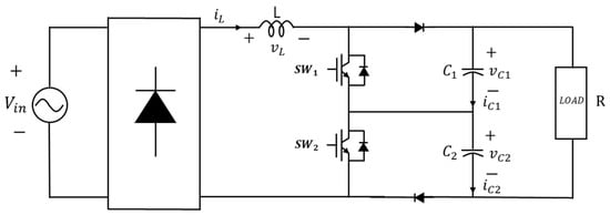
Figure 1.
The circuit diagram of TL PFC converter.
The dynamic mathematical model of the TL PFC converter can be obtained by analyzing the switch operations. The equivalent circuit of the TL PFC converter is divided into four operating states according to the switching operation, as shown in Figure 2. The state when both switches, SW1 and SW2, are off is shown in Figure 2a. The state when SW1 is on while SW2 is off is shown in Figure 2b. The state when SW1 is off, and SW2 is on is shown in Figure 2c. Finally, Figure 2d depicts the state when both switches, SW1 and SW2, are on.

Figure 2.
TL PFC converter switching operation circuit.
The average state space equation can be derived by analyzing the operation mode determined by the duty boundary of 0.5. When the duty cycle is less than 0.5, it is defined as Mode 1. The operating sequence for Mode 1 is State 1 → State 2 → State 1 → State 3, as depicted in Figure 3a. Conversely, when the duty cycle is greater than 0.5, it is defined as Mode 2. The operating sequence for Mode 2 is State 4 → State 3 → State 4 → State 2, as shown in Figure 3b. Since the system control involves two operation modes with a duty boundary of 0.5, it is necessary to analyze their operations for both modes. The state space equations for each state are summarized in Table 1.
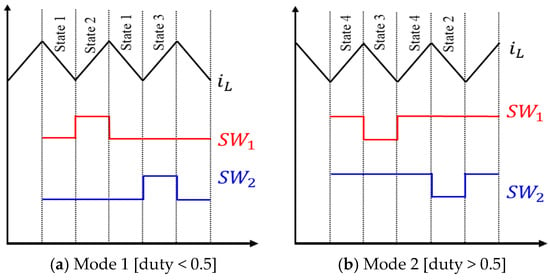
Figure 3.
Mode operation by duty range.

Table 1.
The summary of the state space equation for each operation states.
The state-averaging equations can be calculated by multiplying the state equations and their operation time for each Mode. The resultant state-averaging equations are the same for Mode 1 and Mode 2 and can be expressed as displayed in (5).
The state-averaging equation of Mode 1 is the same as that of Mode 2, which means that mode transition does not need to be considered when designing the controller. This means that the above equation can be applicable to the full duty range. However, since the above equation includes duty, that is, a variable that changes with time, linearization at the operating point is necessary [,,,,]. By applying small signal perturbation for linearization at the operating point, the following linearized equation can be obtained:
If assuming that capacitor and are equal in the small signal analysis equation, it can be expressed as a quadratic equation, and, thus, a simple controller design is possible. The capacitor imbalance occurs in actual applications. Therefore, the capacitor voltage balancing controller is required for the reduced quadratic equation. The balancing controller design is shown in the controller design section. The final linearized state space equation is shown as follows:
And the derived steady-state DC values of , are shown in (8).
The input–output transfer function equation for voltage and current controller design can be obtained from the Laplace transform and is shown in the following equations from (9) to (11):
3. Double-Loop Controller Design
The configuration of the single-phase PFC controller consists of a double-loop structure, as illustrated in Figure 4. It comprises a voltage controller for regulating the DC output voltage in the outer loop and a current controller for ensuring the power factor remains close to unity by controlling the current of the AC input terminal as a sine wave in the inner loop. In single-phase PFC control, the Proportional-Integral (PI) controller cannot be directly applied to the current controller because the current waveform is sinusoidal, not DC. Conventional methods often use an instantaneous AC current controller that adopts a Proportional (P) controller. However, these methods may fail to achieve zero steady-state error and can be problematic when there are abrupt changes in the command or disturbances in the environment.

Figure 4.
Double-loop controller configuration.
To achieve zero steady-state error, a PI current controller using DQ transformation can be applied. However, this transformation typically requires at least two sources, which poses a challenge in single-source systems. To overcome this limitation, a virtual 90-degree phase-shifted signal is created. This can be achieved by using a virtual power source or implementing a filter such as an All Pass Filter (APF) []. This paper explores the use of APF to facilitate single-phase DQ conversion.
The detailed control block diagram of the outer loop, regulating the output voltage, and the inner loop, controlling the inductor current, is depicted in Figure 4. The output of the voltage controller, (inductor current reference), is generated through voltage control at the DC output stage. However, in single-phase PFC, voltage ripple occurs at twice the AC input power frequency and manifests in the DC link voltage [,]. This ripple not only complicates voltage control but also impacts current control, posing challenges in designing single-phase PFC controllers and determining PI gain values. To address this issue, this paper proposes the use of a band-stop filter in voltage control to suppress the 120 Hz DC voltage ripple. The equation for the Band-stop filter is expressed in (12).
From (12), the equations for the stop-band frequency, B and , can be obtained through (13) and (14), respectively. represents the stop-band frequency, and represents the reference frequency [].
By using (13) and (14), the values corresponding to each frequency can be calculated. The transformation from the s-domain (continuous) to the z-domain (discrete), is shown in (15) which is derived by substituting s with in the s-domain equation and expanding it.
The 120 Hz ripple can be effectively removed using a band-stop filter, as described by Equation (15). The selected parameters are = 9.55 [Hz] and = 120 [Hz]. Equation (15) has been implemented on a microcontroller, such as a Digital Signal Processor (DSP), using C-code programming. The filter can be applied to both 50 Hz and 60 Hz frequencies by adjusting the parameters of the band-stop filter (BSF). While the manuscript focuses on 60 Hz operation due to its relevance to the grid system used, the flexibility to accommodate both frequencies is noted. Adjusting the BSF parameters enables straightforward adaptation to 50/60 Hz operation.
For the design of the voltage controller, specifications are set with a phase margin of 90 degrees and a bandwidth of 50 [rad/s]. The optimal gains that satisfy these design specifications are automatically determined using the MATLAB SISOTOOL library. The transfer function of the final designed voltage controller can be expressed as shown in Equation (16).
The resultant Bode plot for the designed voltage controller is presented in Figure 5. It can be observed that the phase margin is 90.1 degrees, and the bandwidth is 50.2 [rad/s], meeting the specified design criteria. Therefore, the stability of the system can be confirmed through the Bode plot analysis.
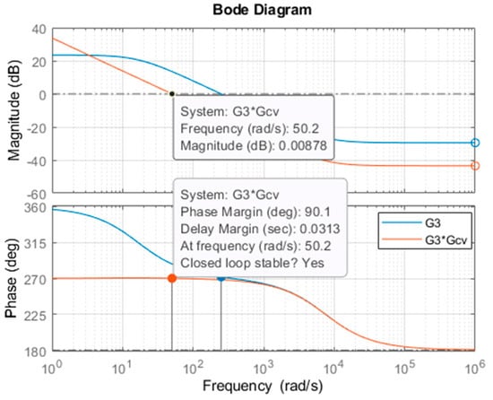
Figure 5.
TL PFC converter voltage controller Bode plot.
In the current control configuration, an APF is used to create a virtual 90-degree phase axis, enabling the design of a single-phase DQ transformation. The APF used in the current controller is a mathematical equation that introduces a phase delay without altering the magnitude of the input signal. It became a transfer function with a magnitude of one across all frequency bands and a phase delay ranging from 0 to 180 deg. (1-pole filter). By utilizing the APF, the actual current axis Iα and the virtual current axis Iβ were generated, as expressed in Equation (17) [,]. The DQ transformation formula based on (17) is described in (18).
In the current control configuration, an All Pass Filter (APF) is employed to generate a virtual 90-degree phase axis, facilitating the design of a single-phase DQ transformation. The APF utilized in the current controller is a mathematical equation that introduces a phase delay while preserving the magnitude of the input signal. It operates as a transfer function with a magnitude of one across all frequency bands and introduces a phase delay ranging from 0 to 180 degrees (a 1-pole filter). By utilizing the APF, both the actual current axis Iα and the virtual current axis Iβ are generated, as expressed in Equation (17). The DQ transformation formula based on Equation (17) is described in Equation (18).
Current control is achieved through the use of an APF and DQ transformation. The design specifications for the current controller are set with a phase margin of 60 degrees and a bandwidth of 4800 [rad/s]. The transfer function of the designed current controller is expressed in Equation (19).
The Bode plot for the current controller is presented in Figure 6. It can be observed from the plot that the phase margin is 60.8 degrees, and the bandwidth is 4820 [rad/s], meeting the specified design criteria. Therefore, the stability of the system can be confirmed through the Bode plot analysis.

Figure 6.
TL PFC converter current controller Bode plot.
The MATLAB m-file, which was used in the controller design, is shown below:
| s = tf(‘s’); Vin = 310; L = 2.4 × 10⁻³; % L = 2.4 mh C = 2400 × 10−6; %C = 2400 µf R = 50; D = 0.311; D1 = 1 − D; Vc = Vin/D1; IL = Vc/(R*D1); G1 = (Vc/L)*(s + 1/(R*C) + (1 − D)*IL/(Vc*C))/(s^2 + s/(R*C)+(1 − D)^2/(L*C)); G2 = −Vin/(L*C)*(−1 + L*s/(R*(1 − D)^2))/(s^2 + s/(R*C) + (1 − D)^2/(L*C)); G3 = (IL/Vc)*(L/C)*(−s + (1-D)*Vc/(L*IL))/(s + 1/(R*C) + (1 − D)*IL/(Vc*C)); Kpv = 1; Kiv = 1; % temporarily set to 1 Gcv = Kpv*(s+Kiv)/s; %wc = 50 [rad/s], P.M = 90 [deg] Kpi = 1; Kii = 1; % temporarily set to 1 Gci = Kpi*(s + Kii)/s; %wc = 4800 [rad/s], P.M = 60 [deg] Vref = Vin/D1; % sisotool Double-loop configuration T = sisoinit (6); T.F.Value = Vref; T.G1.Value = G1; % current loop G1 = (iL/d) T.C2.Value = Gci; % current controller PI = (d/ie) T.G2.Value = G3; % voltage loop tf. = (Vc/iL) T.C1.Value = Gcv; % voltage controller PI = (Iref/Ve) sisotool (T); |
The MATLAB step response of the DC link voltage is depicted in Figure 7. As expected from the design requirements, the waveform of the DC link exhibits no overshoot. The rising time, defined as the time from 10% to 90% of the waveform, is measured as 0.0443 s, while the settling time is found to be 0.0812 s.

Figure 7.
Voltage step response characteristics in MATLAB.
The capacitor balancing controller can be designed from the following equations:
From the above equations, the following relationship can be obtained:
The capacitor voltage difference equation over duty difference can then be rewritten as follows:
where, .
The closed-loop transfer function of the capacitor voltage difference is given as follows:
where, .
The controller configuration of the balancing controller is illustrated in Figure 8a, while its real implementation is depicted in Figure 8b. The controller gain is set to 0.1 based on the design using MATLAB SISOTOOL.

Figure 8.
Capacitor balancing controller.
4. Simulation
The controller was designed using the parameter values shown in Table 2, and the controller design was verified by the PSIM simulation.

Table 2.
Controller system parameter.
Figure 9 displays the waveforms of the AC input voltage and AC current from the double-loop controller. It is evident that the power factor (PF) was stably controlled at 0.9932, which is very close to unity.

Figure 9.
The waveforms of the AC input voltage and AC current.
In Figure 10, the waveforms of the voltage step-up from 450 V to 550 V are presented. Both the output voltage and current are observed to be stably controlled in the boosting section. The actual voltage waveform closely matches the design requirements, except for the 120 Hz ripple components, as shown in Figure 10.

Figure 10.
The waveforms of voltage step-up (PSIM simulation).
The control performance for the load variation is shown in Figure 11. This waveform demonstrates the control performance when the load resistance is changed from 25 Ω to 50 Ω and back. Comparing Figure 9 and Figure 10 confirms that the control remains stable even after load changes.
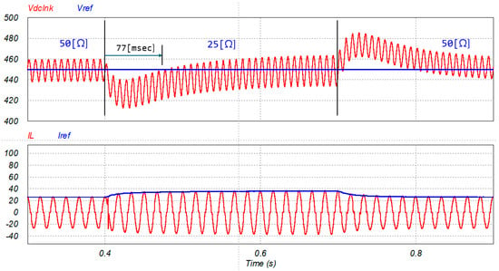
Figure 11.
TL PFC converter control performance waveform for load variation.
The waveforms of the balancing controller are depicted in Figure 12. Capacitors C1 and C2 are set to 1200 [µF] and 2400 [µF], respectively. The difference in capacitance results in a voltage difference between the capacitors, as shown in Figure 12a. This imbalance can be controlled using the balancing controller, the waveform of which is illustrated in Figure 12b.
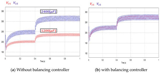
Figure 12.
The waveforms of the balancing controller.
5. Experiments
The hardware is constructed based on the simulation environment. The Texas Instruments’ 320F28069 DSP is utilized for the micro-controller, and the circuit components used in the experiment are configured to match the values presented in Table 1. The detailed setup of the experiment is depicted in Figure 13. While single-phase AC power at 220 V is used in the PSIM simulation, due to limitations in the experimental system’s power, a reduced voltage rating of 110 V is employed during the experiments.

Figure 13.
Hardware setup used in the experiment.
First, the step-up and step-down control for output voltage response characteristics are depicted in Figure 14 and Figure 15, respectively. Figure 14 illustrates the result of boosting the output voltage from 150 V to 210 V, with both voltage and current stably controlled without overshoot. Similarly, Figure 15 displays the waveform resulting from stepping down the output voltage from 210 V to 150 V, where both voltage and current are observed to be stably controlled without overshoot.

Figure 14.
Voltage and current waveforms for reference voltage from 150 V to 210 V.
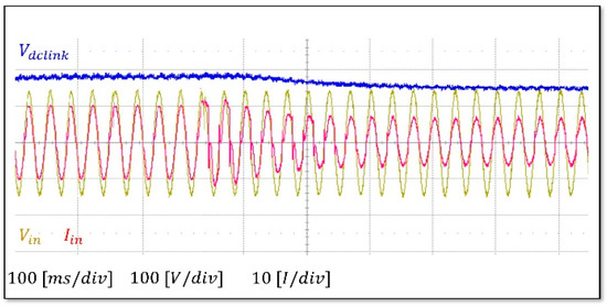
Figure 15.
Voltage and current waveforms for reference voltage from 210 V to 150 V.
Figure 16 shows the waveform when changing the load resistance from 50 Ω to 25 Ω, and Figure 17 shows the waveform when changing it from 25 Ω to 50 Ω. In both cases, it was observed that the voltage was stably controlled. However, with regard to the current, fluctuations were initially observed, but the control stabilized within a short period of time.
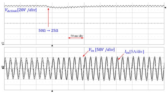
Figure 16.
Waveforms for the load change (50 → 25 [Ω]).
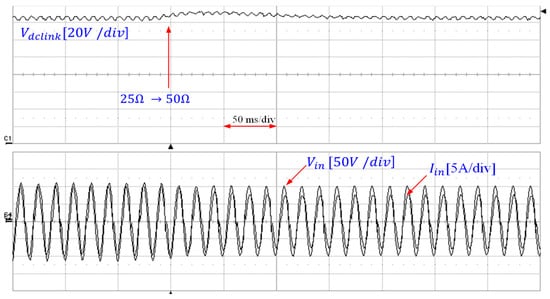
Figure 17.
Waveforms for the load change (25 → 50 [Ω]).
The waveforms obtained through the actual experiment closely match the PSIM simulation results, confirming the theoretical validity of the proposed modeling and controller design through experimentation.
6. Conclusions
The paper proposes a double-loop controller design technique to enhance the modeling of a 3-level power factor correction (PFC) converter. The research aims to address challenges encountered in existing single-phase PFC circuits, particularly concerning the presence of a 120 Hz ripple voltage. Prior studies have not adequately addressed double-loop controller design or voltage ripple rejection in this context. Therefore, this paper presents a novel approach by applying a 3-level structure to achieve these goals.
The proposed technique involves configuring the obtained state space expression of the transfer function to be applicable across the full duty range. Subsequently, a double-loop controller is designed using MATLAB SISOTOOL. To evaluate the effectiveness of the proposed controller, verification is conducted through PSIM simulation. Moreover, the proposed controller is implemented in practice, and the efficacy of the system design is confirmed through experimental validation.
The primary contribution of this paper is demonstrating the controllability of the double-loop controller for a three-level PFC converter under varying operating points. This highlights the capability of the proposed controller to maintain operation across the entire duty cycle range, achieving unified control. This achievement distinguishes our work, as previous research has not explored this comprehensive aspect.
Author Contributions
Equally contributed. All authors have read and agreed to the published version of the manuscript.
Funding
This research was supported by “Regional Innovation Strategy (RIS)” through the National Research Foundation of Korea(NRF) funded by the Ministry of Education(MOE)(2021RIS-001). This work was supported by the Human Resources Development of the Korea Insitute of Energy Technology Evaluation and Planning(KETEP) grant funded by the Korea government. (No. 20224000000070).
Data Availability Statement
Data are contained within the article.
Conflicts of Interest
The authors declare no conflict of interest.
References
- Lee, K.-M.; Kim, I.-S. An Study on the Improved Modeling and Double-loop Controller Design for Three-Level Boost Converter. Trans. Korean Inst. Power Electron. 2020, 25, 442–450. [Google Scholar]
- Pahlevani, M.; Eren, S.; Bakhshai, A.; Jain, P. A DC-bus voltage control technique for grid-connected AC/DC converters used in smart energy storage units. In Proceedings of the 2015 IEEE 6th International Symposium on Power Electronics for Distributed Generation Systems (PEDG), Aachen, Germany, 22–25 June 2015; pp. 1–7. [Google Scholar]
- Lee, J.-Y.; Chae, H.-J. 6.6-kW Onboard Charger Design Using DCM PFC Converter With Harmonic Modulation Technique and Two-Stage DC/DC Converter. IEEE Trans. Ind. Electron. 2014, 61, 1243–1252. [Google Scholar] [CrossRef]
- Ryan, R.T.; Hayes, J.G.; Morrison, R.; Hogan, D. Digital control of an interleaved BCM boost PFC converter with fast transient response at low input voltage. In Proceedings of the 2017 IEEE Energy Conversion Congress and Exposition (ECCE), Cincinnati, OH, USA, 1–5 October 2017. [Google Scholar] [CrossRef]
- Kim, J.-S.; Kang, J.-I.; Cho, J.-H.; Lee, J.-H.; Ahn, H.-M. DC-link voltage fluctuation compensating algorithm for PFC input voltage magnitude variation. Power Electron. Conf. 2023, 465–466. [Google Scholar]
- Ciobotaru, M.; Rossé, A.; Bede, L.; Karanayil, B.; Agelidis, V.G. Adaptive Notch Filter Based Active Damping for Power Converters Using LCL Filters. In Proceedings of the IEEE 7th International Symposium on Power Electronics for Distributed Generation Systems (PEDG’16), Vancouver, BC, Canada, 27–30 June 2016. [Google Scholar]
- Yang, D.; Choi, D.; Shin, J.; Choi, B. Stability Analysis of Boost PFC Considering the External Impedance. Power Electron. Conf. 2023, 255–257. [Google Scholar]
- Jeong, S.-W.; Lim, J.-H.; Lee, D.-I.; Hyeon, Y.-J.; Lee, S.-Y.; Kim, W.-J.; Youn, H.-S. PFC DC/DC Integrated Converter for High Density of On-Board Charger. Power Electron. Conf. 2023, 550–551. [Google Scholar]
- Kim, S.-H.; Cha, H.-N.; Kim, H.-G.; Choi, B.-C. Clamp-mode Three-level High Voltage Gain Boost Converter using Coupled Inductor. Trans. Korean Inst. Power Electron. 2012, 17, 500–506. [Google Scholar] [CrossRef][Green Version]
- Barazarte, R.Y.; González, G.G. Design of a Two-Level Boost Converter. In Proceedings of the Eleventh LACCEI Latin Acmerican and Caribbean Conference for Engineering and Technology, Cancun, Mexico, 14–16 August 2013; pp. 1–8. [Google Scholar]
- Kim, I.S. Power Conversion Controller Design (Using PSIM and MATLAB); Hongneung: Seoul, Republic of Korea, 2023. [Google Scholar]
- Keskin, A.; Pal, K.; Hancioglu, E. Resistorless first-order all-pass filter with electronic tuning. AEU Int. J. Electron. Commun. 2008, 62, 304–306. [Google Scholar] [CrossRef]
- Song, M.-G.; Lee, W.-C. A Study on the DC-Link miniaturization and the Reduction of output current distortion rate by Reducing the Effect of 120Hz Ripple Voltage on Photovoltaic Systems. Power Electron. Conf. 2020, 166–167. [Google Scholar]
- Sim, W.; Jo, J.; Kim, Y.; Cha, H. Reactive power control of single-phase reactive power compensator for distribution line. Trans. Korea Inst. Power Electron. 2020, 25, 73–78. [Google Scholar]
- Ben Haddi, S.; Zugari, A.; Zakriti, A.; Achraou, S. Design of a Band-Stop Planar Filter for Telecommunications Applications. Procedia Manuf. 2020, 46, 788–792. [Google Scholar] [CrossRef]
- Zhang, R.; Cardinal, M.; Szczesny, P.; Dame, M. A grid simulator with control of single-phase power converters in D-Q rotating frame. In Proceedings of the 2002 IEEE 33rd Annual IEEE Power Electronics Specialists Conference, Cairns, Australia, 23–27 June 2002; pp. 1431–1436. [Google Scholar]
- Park, H.C.; Kim, I.S. Optimal Gain Design Method of the 3 Phase Boost Converter. Trans. Korean Inst. Power Electron. 2017, 22, 1–8. [Google Scholar] [CrossRef][Green Version]
Disclaimer/Publisher’s Note: The statements, opinions and data contained in all publications are solely those of the individual author(s) and contributor(s) and not of MDPI and/or the editor(s). MDPI and/or the editor(s) disclaim responsibility for any injury to people or property resulting from any ideas, methods, instructions or products referred to in the content. |
© 2024 by the authors. Licensee MDPI, Basel, Switzerland. This article is an open access article distributed under the terms and conditions of the Creative Commons Attribution (CC BY) license (https://creativecommons.org/licenses/by/4.0/).