Article

Operational Amplifiers Defect Detection and Localization Using Digital Injectors and Observer Circuits

ECpE Departments, Iowa State University, Ames, IA 50011, USA
*
Author to whom correspondence should be addressed.
Electronics 2024, 13(14), 2871; https://doi.org/10.3390/electronics13142871 (registering DOI)
Submission received: 11 June 2024 / Revised: 15 July 2024 / Accepted: 17 July 2024 / Published: 21 July 2024

Abstract

:
Operational amplifiers (op amps) are fundamental blocks that find wide application both as stand-alone devices and as crucial blocks embedded in various Systems on Chips (SoCs). Achieving high defect coverage, as well as performing defect localization in these circuits, has proven to be a difficult/expensive task, even with sophisticated testing circuitry. The ISO 26262 standard for functional safety (FuSa) includes the stringent requirement that an automotive IC must have a very high defect coverage. This reinforces the need to ensure the functionality of analog and mixed (AMS) circuits, especially in mission critical applications. This paper presents an all-digital op amp defect detection, diagnosis, and localization method that can be used both for production and in-field tests and discusses various implementation of the proposed method. We validated our results using extensive transistor-level simulations of multiple op amp architectures using TSMC 180 nm technology. Across op amp architectures and multiple implementation approaches, we achieved a worst-case and best-case defect coverage of 94.5% and 99%, respectively. Furthermore, in this work, we also propose a defect diagnosis and localization strategy using recorded bit streams from states of digital injectors and detectors.

1. Introduction

The increase in the demand for advanced features and functionalities, among several other factors, has led to a rapid increase in the level of integration of semiconductor chips into applications in the automotive, space, health, and other mission critical industries. On the other hand, the extensive integration of these chips also increases their complexity and can introduce new points of failure. The development of cost-efficient novel defect detection strategies is becoming one of the hot topics in the semiconductor industry [1]. Defect detection is a multifaceted problem. On one hand, the ISO 26262 standard [2] for functional safety recommends that an automotive IC have a high defect coverage (>90%). However, rigorous testing schemes require a long testing time, thereby significantly impacting the overall test cost [3] and invariably also increasing the production cost. Furthermore, most of the failures in ICs reported in customer returns are in-field ICs that have failed due to latent defects [4], emphasizing the significance of developing testing schemes that can be implemented for in-field testing. In addition to this, once latent defects or any form of defects are detected, it is crucial to locate the source of the defect to improve future circuit designs and make them more reliable.
The main components of commonly used IP blocks on an SoC are AMS circuits, digital circuitry, and memory logic. Due to the relative ease of defect diagnosis in digital circuits, coupled with extensive research backed by unifying standards, defect detection in digital circuits has made significant progress [5]. As a result, digital circuits are responsible for only 20% of reported failures in ICs, even though they make up 80% of all systems [5,6]. This demonstrates the significant role that AMS defect detection strategies must play in improving overall IC reliability. Op amps represent one of the most versatile blocks in AMS ICs and possibly the most commonly used [7], making the addressing of defect detection concerns in them a pressing need. In literature, several op amp defect detection methods have been proposed to solve these challenges.
In [8,9], the authors have proposed defect testing frameworks that reduce the simulation test time and save test costs. In ref. [8], the authors achieve time savings in simulations by sweeping a global control variable and, as a result, avoiding the repetitive work of generating a netlist for each defect. Refs. [10,11] also proposed methods to group/cluster defects in an analog circuit and consequently reduce the number of test simulations and the test time. Others [12,13] also utilize the multi-site testing capabilities of modern automated test equipment (ATE), where numerous devices are simultaneously tested on a single board to reduce the test time. Recently, several design for test (DFT) and built-in self-test (BIST) methods [1,7,9] have been proposed as strategies to ensure the continued reliability of ICs through online health monitoring. Several op amp defect detection methods [3,14,15,16,17,18,19,20] have also been proposed in literature. In refs. [14,15,16], an op amp circuit under test (CUT) is converted to an oscillator using passive networks for defect testing. Refs. [17,18] proposed op amp defect testing by monitoring quiescent and/or transient supply current while [19,20] also proposed a method to test op amps through a DC voltage sweep.
This paper, which is a further development of the concept introduced in [7], presents a simple defect-oriented testing technique for op amp defect detection, diagnosis, and localization. The major contributions in this paper are as follows:
  • This manuscript provides a more extensive explanation of Intentional Offset Injection (IOI) op amp defect detection and shows, by way of analytical formulas, how to realize robust testing circuitry.
  • We demonstrate how to apply intentional offset injections to all possible offset injection sites for a given op amp architecture and validate with simulation results.
  • In this manuscript, we discuss a novel defect localization technique for op amps using a binary sequence obtained from the state of the digital injectors and detectors employed in our method after testing.
The rest of the paper is organized as follows. In Section 2, we provide clarity on certain defect terminologies used throughout this paper and in literature, along with a review of existing op amp defect detection techniques. We also present our defect model. In Section 3, we discuss our proposed method of using purely digital testing circuitry as a control and an observer circuit to detect, diagnose, and localize defects in the op amp, Widlar reference, and bias circuitry. Section 4 presents the simulation results for two circuits under test (CUTs), while Section 5 outlines our conclusions.

2. Literature Review

2.1. Defect Terminology Review

  • A fault is an unexpected change in a specified performance of a primitive circuit or circuit module that is not within the circuit’s specification limits [21].
  • A defect is an unintended physical change in the manufactured circuit that causes a difference between the fabricated circuit and its layout. Defects are of two types: hard and soft defects.
  • A soft defect, also called a parametric defect, does not affect the circuit topology but translates to variations in the component parameters that affect its output. They result from imperfections in IC fabrication, causing variations in oxide thickness, substrate doping, threshold voltage, mobility, and transistor width [14].
  • Hard (catastrophic) defects, on the other hand, are those that change circuit topology. They are generally introduced by local defect mechanisms such as impure particles on the wafer surface, defects in oxide, dust particle interaction during masking, which blocks the exposure, etc. Hard defects usually result from short and open defects in circuit components. The defect detection techniques presented in this work primarily focus on catastrophic defects, as they make up about 80% of observed analog faults [20].
  • The defect universe refers to all reasonably likely defects that can be algorithmically defined, excluding those in unused circuitry.
  • The defect model is an equivalent circuit for a defect in the context of a circuit simulator. In this work, the defect models for testing defects are in line with P2427 standards [21].
  • The defect coverage is the weighted percentage of defects detected by tests applied to the circuit’s ports as a fraction of all defects in the circuit’s defect universe. Although it is not the only metric, a high defect coverage is one of the hallmarks of a good defect detection and diagnosis strategy.
% D e f e c t   C o v e r a g e = W e i g h t e d   t o t a l   n u m b e r   o f   d e f e c t s   d e t e c t e d A l l   d e f e c t s   i n   c i r c u i t s s   d e f e c t   U n i v e r s e × 100
  • Defect localization is the mapping out of the physical region of the circuit where the defect occurred.
  • Defect collapsing comprises grouping defects that have the same effect. Defect collapsing serves as a good basis to reduce the amount of defect testing simulation by simulating a few samples in each cluster.

2.2. Defect Model

The defect detection strategy presented in this paper focuses on short and open hard defects. In accordance with the model prescribed in P2427 Standards [21], we test the six common transistor defects (Drain Open, Source Open, Gate Open, Gate-Drain Short, Gate-Source Short, Drain-Source Short) shown in Figure 1 and Figure 2, along with open and short defects in passive elements (resistors and capacitors), shown in Figure 3. Although we considered only catastrophic defects, to ensure robustness, we tested our method with strong shorts (1 Ω), as well as intermediary shorts (10 Ω) and light shorts (100 Ω). For open defects, resistors of 5 MΩ (light open), 50 MΩ (intermediate open), and 500 MΩ (strong open) are used. These defects are injected into our circuit under test (CUT) under the single-fault assumption [17]. For detailed information on the defect models used in this manuscript, readers can refer to reference [9].

2.3. Op Amp Defect Testing Methods in Literature

Several defect testing strategies for op amps have been presented in literature over the years [3,14,15,16,17,18,19,20]. In this subsection, we discuss two of the op amp defect testing techniques that have been proposed.

2.3.1. Oscillation Test Methodology (OTM)

OTM involves converting a CUT into an oscillator using either external “RC” components (for production testing) or internal “RC” components (for built-in self-test approach). The oscillation frequency of the circuit is then compared to an upper and lower frequency threshold expected in a defect-free circuit (herein after referred to as a golden circuit) based on process and mismatch variations. If the measured frequency is within this threshold, then the circuit is considered to have no defect; otherwise, it is characterized as defective. References [14,15,16,19] have all proposed op amp defect detection based on OTM. A drawback to using this technique for op amp defect detection is that it requires area-intensive resistors and capacitors to convert CUT into an oscillator. Also, OTM is a transient-based test scheme and, as such, requires more simulation time. The long test time coupled with the area-intensive testing circuitry needed to execute OTM make it an expensive test method. We present an op amp defect detection method based solely on DC parametric sweep simulations. Our proposed method requires a few transistors and digital CMOS inverters, which take up a small area compared to resistors and capacitors.

2.3.2. IDDQ and IDDT Testing

In [17,18,22], the authors presented op amp defect detection methods based primarily on monitoring the variations in the transient and/or quiescent supply current of a CUT. IDDQ and IDDT are widely used defect testing techniques discussed in literature. However, the reported results suggest that to achieve a high coverage (92%, as presented in [17]), both transient (IDDT) and quiescent (IDDQ) current measurements must be implemented. Meeting this strict requirement demands the use of intricate testing circuitry, which may not be preferable. Moreover, the need for transient current testing prolongs the defect simulation time, significantly adding to the test cost. Our approach relies primarily on DC testing, which reduces the simulation time required and achieves higher defect coverage.

3. Proposed Testing and Localization Technique

In this section, we discuss how we use injector circuits to control an op amp into a region of operation where the behavior of a defective circuit can easily be distinguished from the golden circuit. In ref. [7], we introduced Intentional Offset Injection (IOI), Widlar reference mismatch injection, and detector circuits for detecting defects in op amps. However, in this paper, we expand on this concept and discuss the various ways in which a designer can utilize this simple and effective tool for defect detection and localization. We also present analytical formulas to back this technique.

3.1. Intentional Offset Injection (IOI)

The main concept of IOI lies in the open-loop transfer function of an op amp, as shown in Figure 4. We define the region bounded vertically by V o s f l t , m a x and V o s f l t , m i n and horizontally by V O L m a x and V O L m i n as the region of operation for a golden circuit, factoring in process and mismatch variations. During the test phase, the IOI testing circuit is used to inject either a positive or negative offset, which is greater than the op amp’s natural (systematic and random) offset and simultaneously observe the op amp’s output with two inverter circuits following one another. In the golden circuit, when a positive offset is injected, the output of the op amp is stuck high, and when a negative offset is injected, the output of the op amp is stuck low. However, through the action of a defect, the op amp offset may be stuck below V o s f l t , m i n or stuck above V o s f l t , m a x regardless of the offset (positive or negative) injected, deviating from the truth table for the IOI method. Table 1 depicts the truth table for IOI.
For a given op amp topology, there are multiple offset contributing sources, but the effects in some areas are more dominant. For instance, in the folded cascode op amp shown in Figure 5, the dominant offset contributing parts are the input differential pairs ( M F 2 , M F 3 ) , cascode-stage top pmos pair ( M F 4 , M F 5 ) , and cascode-stage bottom nmos pair ( M F 10 , M F 11 ) . Similarly, for the telescopic cascode architecture shown in Figure 6, the input differential pairs ( M T 2 , M T 3 ) and the bottom nmos pair ( M T 8 , M T 9 ) are the dominant sources of offset. These are all points at which we can intentionally inject offset for defect detection with the IOI method.
The op amp’s offset after fabrication is made up of a systematic part and a random part. The random offset is a function of several random process parameters ( μ ,   C o x , V t h , e t c ) . This makes the offset after fabrication nearly impossible to predict, but its distribution can be accurately predicted. The randomness in the offset results from mismatch in the op amp’s input pair drain current [23]. For a given folded cascode architecture, the offset after fabrication can be estimated using (1) [23] and its variance deduced from (1) is shown in Equation (2).
V O S V t h 2,3 + g m 4,5 g m 2,3 V t h 4,5 + g m 10,11 g m 2,3 V t h 10,11 + I g m 2,3 β 2,3 β 2,3 + β 4,5 β 4,5 + 2 β 10,11 β 10,11
σ V O S 2 = σ V t h 2,3 2 + g m 4,5 I D 4,5 g m 2,3 I D 4,5 2 σ V t h 4,5 2 + 2 g m 10,11 I D 10,11 g m 2,3 I D 2,3 2 σ V t h 10,11 2 + 1 g m 2,3 I D 2,3 2 σ β 2,3 β 2,3 2 + σ β 4,5 β 4,5 2 + 4 σ β 10,11 β 10,11 2  
For this analysis, assume I = I D 2,3 = I D 4,5 = 0.5 I D 10,11 . It is important to remember that in MOS technology, the variance of a process parameter p , between two identical adjacent transistors, reduces inversely with the gate area and is shown in (3) [24]. By using (3), we can accurately determine the variance of both the threshold voltage ( V t h ) and the transconductance parameter β and, by extension, the variance of the op amp’s post-fabrication offset. Similar analysis can be performed for other op amp topologies. By estimating the standard deviation, we can determine the aspect ratio ( W / L ) of the IOI testing transistors to ensure that for a certain yield level, we can guarantee that IOI will inject positive and negative offset.
σ p = A p A

3.2. Compensation Network

For defect detection in the compensation network, we use the simple rise and fall time introduced in [3]. The main idea in this method is that an open defect in a compensation network can lead to much lower rise/fall times compared to a defect-free op amp. This reduction in rise/fall times is detected using simple digital control and monitor circuits. This method is explained more elaborately in Results (4.1.2).

3.3. Widlar Mismatch Injection

We introduced Widlar mismatch injection in [7] to detect defects in the Widlar current reference and the bias circuit. The basic principle in the Widlar mismatch injection is to intentionally skew the current mirror ratio in the Widlar reference during the test phase to set it into a certain operating condition where the action of a defect is easily detected. From Figure 6, we can see that there are multiple current mirrors, each of which is a potential injection site for Widlar mismatch injection. However, considering M W 1 and M W 2 is the first point of the signal path, makes it the best skewing point. During the test phase, the source of the transistor M W I D (blue in Figure 6) is connected to V D D to alter the current mirror ratio and observer circuit are used to monitor the bias voltage V b p , V b n , and V p t . During normal operation, M W I D is turned off to restore the current mirror ratio. As such, the testing circuit has no effect on the op amp’s operation.

3.4. Detectors

In our proposed defect detection and localization approach, we use the simple digital CMOS inverters and digital window comparators introduced in [7]. A CMOS inverter produces an output signal opposite to the input signal by comparing it against its switching threshold. The switching threshold of an inverter is determined by the aspect ratios of the nmos and pmos transistors. Increasing the aspect ratio of the pmos increases the switching threshold, and vice versa. Similarly, increasing the aspect ratio of the nmos reduces the inverters switching threshold, and vice versa. These inverters are designed such that the switching threshold is around the mid-point of V D D and V S S at a typical corner. In our defect testing setup, we place two inverters to directly follow each other (Figure 6) at the output of the op amp to convert analog signals that are close to V D D to digital ‘1’ and the analog signals that are close to V S S as digital ‘0’.
The second detector implemented in our testing circuitry is the digital window comparator shown in Figure 7. Unlike an analog window comparator that requires two references, in the digital window comparator, an analog input signal is compared to two switching thresholds, V T H and V T L , of the H I N V and L I N V inverters, respectively. If the signal lies within the thresholds, then the output from the XOR will be a digital high; otherwise, it will be a digital low (see Table 2).

3.5. Proposed Defect Localization Method

As has already been emphasized, the defect detection strategy presented in this paper focuses on short and open hard defects. Short defects create an additional conductive electrical path between two (or more) nodes in the defect-free netlist, whereas open defects break a connection between two (or more) terminals of one or more circuit elements in the defect-free netlist. Due to the difference in their impact on the circuit, our proposed approach investigates defect localization in short defects and open defects separately.

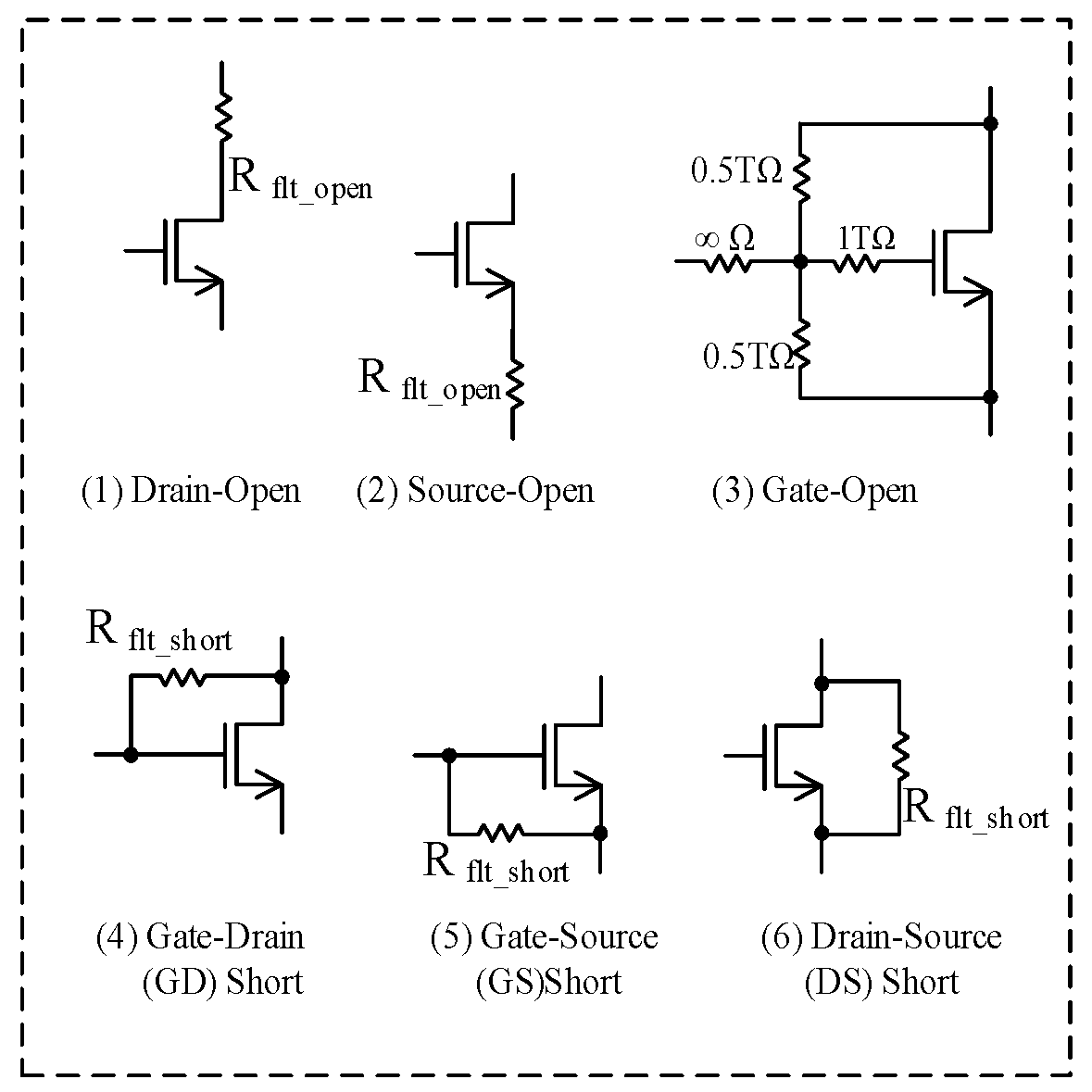
3.5.1. Localization Approach for Short Defects

The proposed defect detection and localization method discussed in this paper implores two injectors and four detector circuits. Considering their digital nature, detectors can have only two different outputs, a ‘1’ and a ‘0’. For the digital window comparator, an output high depends solely on the placement of the window. For each of the injector controls (IOI and Widlar mismatch), each detector outputs a 2-bit binary made of any combinations of 0s and 1s. Thus, for both control injections, each detector records a 4-bit binary stream. Consequently, at the end of the testing phase, for four detectors, we obtain a 16-bit binary number. These 16-bit binary streams correspond to unique decimal values, and all the defects that map to these values are clustered together and can be used to point out where defect occur in the circuit. This information can also be used to reduce the test time by testing a few samples from individual clusters, as opposed to testing all defects in the defect universe for subsequent defect testing.

3.5.2. Localization for Open Defect

An open defect ( f n ) , leads to a high impedance, breaking the connection between two or more nodes. Consequently, the current in these high-impedance paths approaches zero. To accurately capture this information for the purpose of localization, we monitor currents on k selected branches ( B ) during the instance of an open defect. These currents, I k i , are compared to an upper and lower current threshold that can flow through the branch in a golden circuit. A digital ‘ 1 ’ is generated for a current within this threshold and a digital ‘ 0 ’ is generated for the opposite case. Like the short defect case, each current branch generates a 4-bit binary stream at the end of testing and a 4 k -bit binary stream for all k monitored branches. All defects that have the same decimal value signature for the 4 k -bit binary stream are clustered together. A simple algorithm depicting the explanation is shown in Algorithm 1. The upper and lower current thresholds for each monitored branch in a defect-free case are obtained through Monte Carlo simulations involving process and mismatch variations.
Algorithm 1: open defect clustering and localization
Open defect list:   F 0 = { f 1 , f 2 , f 3 , , f n }
Control injector states:  S 0 = { s 1 , s 2 , s 3 , s 4 }
Branches to monitor:  B = b 1 , b 2 , b 3 , , b k
for each defect  f n in defect list:
     Carry out defect simulation and obtain branch current for all 4 states.
     for each element  b k B :
         for all 4 states: generate 4- bit binary.
                         If node current,  I k i  is within limit  I k i , u p p e r  and  I k i , l o w   then;
                        Bit = 1
                Else:
                                Bit = 0
Compute Decimal equivalence  D f  of 4k-bit binary streams due to defect  f n  
for all  f n   F 0  do
              If they have the same, D f  then;
                      place in one group.

4. Defect Simulation Results

In this section, we present extensive transistor-level simulation results validating the proposed op amp defect detection and localization technique using two CUTs: a two-stage folded cascode amplifier and a two-stage telescopic op amp. Multiple op amp defect detection techniques [14,25] presented in literature are tested against the simple five-transistor differential amplifier followed by a common-source (CS) stage and, as such, do not include defect detection in cascode transistors, which are common to several high-performance op amp topologies. As discussed in Section 3.1, for a particular op amp topology, there are multiple sites for offset injection that a designer can select. To show the universality of the proposed method, we present results for all IOI sites for a given op amp topology. All designs were done using 1.8V I/O transistors in TSMC 180 nm technology.

4.1. Simulation Results for Telescopic Op Amp

Figure 6 shows the complete schematic of a two-stage telescopic op amp, while Figure 8 shows the frequency response of the amplifier in a typical corner. The systematic offset is 3.06   μ V , and its standard deviation is 1.28   m V . During normal operation, the offset injection switches M I O I P O S and M I O I N E G are opened. Similarly, the drain of M W I D is grounded to ensure a mirror ratio of 1:1 for M W 1 and M W 2 . As a result, the testing circuit has a negligible effect on the normal operation of the op amp and consumes negligible power.

4.1.1. Defect Detection in Telescopic Op Amp (Main Structure)

During defect detection, the op amp is set into an open-loop configuration, while V N and V P are also set to a common mode voltage, V C M . By setting either V O S N E G or V O S P O S high to close switches M I O I N E G and M I O I P O S , respectively, the matching of the differential pair ( M T 2 , M T 3 ) is skewed to introduce offset. As has already been discussed, when both input voltages ( V N and V P ) are set to some common-mode voltage, any injected offset should be amplified and should produce an appropriate output. Specifically, injecting a positive offset should result in a ‘1’ at V O U T D I G , and injecting a negative offset should result in a ‘0’ at V O U T D I G . However, under the presence of a defect, say, DS short of M F 13 , the output of the amplifier is drawn closer to V S S , setting the V O U T D I G to a logical ‘0’. This situation persists regardless of a positive or negative injected offset, violating the truth table.
The explanation provided above is the same for IOI through other sites. Using the single-fault assumptions [7,17], we injected all defects in the defect universe based on the defect models presented in Section 2. For the 11 transistors in the main amplifier, we injected 66 defect cases. The results show a high coverage, 66/66 (100%) and 63/66 (95%), for offset injection through the differential pair and bottom nmos pair, respectively. Table 3 provides a summary of the results for IOI for all injection sites.

4.1.2. Defect Detection in Compensation Network

The main purpose of the compensation network is to keep the op amp stable, with little to no oscillatory behavior. The capacitor Cc and the nulling resistor Rz in Figure 6 form the compensation network. In this work, to detect the defects in the compensation network (Cc, Rz), we use a similar rise/fall time-based method, presented in [3]. In DC, as a capacitor behaves like an open circuit as such, it is not possible to test the functioning of a capacitor with just DC simulations alone. Using a simple bitstream-based test, as tabulated in Table 4, we can test the defects in the compensation network.
The fundamental idea with this method is that when the compensation network has no defects; the rise/fall time of the operational amplifier is high as compared to the op amp with defects in the compensation network. The fall time for a defect-free op amp is way higher than an op amp with open defects in the compensation network. Using this information, if we keep the bit width of the bitstream less than T d e l t a , then the defects in the compensation network are detected where T d e l t a is defined as the difference between the delay of a defect-free device and that of a device with an open defect in the compensation network. This is shown in Figure 9. For our CUT, T d e l t a = 64   μ s . The truth table in Table 4 is tested by setting T b i t = 10   μ s , which is nearly ( 1 / 6 ) t h of T d e l t a . As shown in Figure 10, the open defects in the compensation network are detected at Bit 3. By performing this test, open defects in Rz and Cc, as well as short defects in Cc, are detected. The only defect that is not detected is a short defect in Rz. The reason for this is that, although a short defect in Rz is a hard defect, the op amp still retains the properties on the compensation, making it an undetectable defect.

4.1.3. Defect Detection in Widlar Reference and Current Bias Circuit

For defect detection in the Widlar reference and bias circuit, we apply the Widlar reference mismatch injection while we monitor the three bias voltages: V b p , V b n , and V p t . We monitor these node voltages using the digital window comparator. The digital window comparator V p t _ w c is designed such that the bias voltage V p t of the golden circuit lies within the window during both control injections, even with its process and mismatch variations. The digital window comparator V b n _ w c is designed such that the bias voltages V b n lies in the window during IOI and lies outside the window during Widlar mismatch injection for all process and mismatch variations, while the digital window comparator V b p _ w c , on the other hand, is designed such that during IOI bias voltage, V b p lies outside the window, and it lies within the window during Widlar mismatch injections. Table 5 summarizes this explanation and shows the digital output state expected from the window comparator for a golden circuit.
During this test phase, we skew the current mirror ratio of M W 1 and M W 2 in the Widlar reference by connecting the drain of transistor M W I D to V D D . Like the case of the main amplifier, we injected defects under the single-fault assumption. For eight transistors and one resistor, we injected 46 defects and obtained a defect coverage of 100%. To ensure robustness and prevent false fails, we performed 200 Monte Carlo simulations of node voltage mismatch and process variations. We also performed 200 Monte Carlo simulations with mismatches and process variations for the transfer characteristics of detectors. Simulation results showing node voltages accurately captured in corresponding windows, regardless of these mismatches and process variations, are shown in Figure 11, Figure 12 and Figure 13.
For the complete op amp and Widlar reference bias circuit, we obtained a coverage of 97% and 99% for IOI injection through a differential pair and bottom nmos pair, respectively.

4.1.4. Defect Localization and Clustering in Telescopic Op Amp

As already discussed in Section 3, the proposed method for defect localization and clustering splits the defect universe into open defects and short defects based on their impact on the op amp. For the localization and clustering of short defects we use the digital states of detectors to form a 16-bit binary value. All short defects that have equivalent 16-bit binary signature are collapsed into a single cluster. Based on the states of the truth tables presented in table detectors, the binary signature of the golden circuit is obtained as “1111110000111010”. Table 6 summarizes the cluster results for short defects in the Telescopic op amp and Widlar reference and current bias circuit for the highest defect coverage results. Localization results for the compensation network are not presented, as they provide unique signatures based on the test approach used.
For open defect localization, we apply the method described in Algorithm 1. We monitored currents in branches I T B 1 I T B 3 in the telescopic op amp and I W B 1 I W B 4 in the Widlar reference and current bias circuit. Based on this, we generated the binary signature of each defect injected. The simulation results for open defects with the same binary signatures clustered together are summarized in Table 7.
From the diagnosis results, we realize that multiple defects can have the same defective signature. In some cases, this is because the defect involves the same nodes. For instance, gate source shorts on any of transistors M T 8 and M T 9 involve a short between the same two nodes and can be expected to be clustered together. In other cases, defects are clustered together because the chain of signal propagation following the incident of a defect has the same effect on the op amp. For instance, an open defect on any of the terminals of transistors M T 10 and M T 11 results in a high-impedance path at the op amp’s second stage, causing the second stage to shut down. Correspondingly, all such defects are clustered together.

4.2. Defect Coverage and Localization Simulation Results for Folded Cascode Op Amp

4.2.1. Defect Detection in FCA

Figure 5 shows the complete schematic of a two-stage folded cascode amplifier. The Widlar current reference and bias circuitry is as shown in Figure 6. Figure 14 shows its frequency response. Like the telescopic op amp, for defect detection in the main amplifier, we apply the IOI method. However, unlike for a Telescopic op amp, there are three sites of possible injection ( M F 2 and M F 3 , M F 4 and M F 5 , and M F 10 and M F 11 ) for this op amp, any of which can be selected, based on the preference of the designer, for IOI defect testing. For the estimated variance of offset using (2), we size the aspect ratio for IOI testing transistors to guarantee that positive and negative offset is injected, ensuring a robust defect detection technique. The 500 Monte Carlo simulations of mismatch and process variations depicting this for a 3-sigma yield is shown in Figure 15.
For the 13 transistors in the main amplifier and 6 defects per transistor, we injected defects from our defect universe, following the single-fault assumption. The simulation results depict a high coverage of 72/78 (92%), 73/78(94%), and 77/78 (99%), for off-set injection through the top pmos pair in the cascode stage, the bottom nmos pair in the cascode stage, and the differential pair, respectively. This is summarized in Table 8. The procedure and simulation results for defect detection in the compensation network, the Widlar reference and current bias circuit, is as outlined in the previous subsection. The final coverage results for complete op amp and all biasing circuit are 95%, 94.5%, and 98% for IOI injection through the top pmos pair, bottom nmos pair, and differential pair, respectively.

4.2.2. Defect Localization in FCA

For defect localization and clustering in the telescopic op amp, we implemented a similar approach to that used inthe telescopic op amp. However, in this architecture, the current branches I F B 1 I F B 7 in the main amplifier and I W B 1 I W B 4 were monitored to obtain the binary signatures of individual defects. The simulation results for short and open defect localization and clusters are presented in Table 9 and Table 10, respectively.

5. Conclusions

We discussed a simple, high-coverage, and robust op amp digital defect detection method and showed, by means of analytical simulations, how to accurately size-test transistors to ensure robust performance across process and mismatch variations. We also introduced a novel defect localization approach using digital states of control and observer circuits in our method. The proposed method was validated with two CUTs. For the folded cascode amplifier, it achieved a worse case coverage of 94.5% and a best-case coverage of 98%. For the telescopic op amp, the proposed method achieved a worst-case coverage of 97% and a best-case coverage of 99%. Our proposed method is low-cost and time-efficient, as it is primarily based on DC simulations. Information obtained from localization can be used for failure analysis tests on part returns and also to help in redundant circuit planning. Moreover, the clustering information generated can help to further reduce the relatively small total simulation/test time of this method in comparison with other methods by simulating few samples from each cluster. Owing to the digital nature of the proposed testing circuitry, it can also easily be implemented with existing digital testing infrastructure, like IJTAG, on an SoC.. Furthermore, the proposed method can also be integrated as part of power-on testing and online health monitoring procedures, thereby ensuring continuous reliability during the IC lifetime. In future work, we are investigating approaches to reduce defects in a single cluster by introducing more digital markers to increase the digital signature of an injected defect.

Author Contributions

M.S. (Michael Sekyere) is the main author and wrote almost all the sections of the manuscript. M.S. (Marampally Saikiran) wrote the portion on defect detection in compensation network, including all simulation work pertaining to it. M.S. (Marampally Saikiran) also worked on editing, and providing constructive feedback on, every part of the manuscript. D.C. is our supervisor. D.C. provided directives on a weekly basis and assisted in shaping the op amp defect detection and localization concept. All authors have read and agreed to the published version of the manuscript.

Funding

Semiconductor Research Corporation (SRC). TASK 2810.084.

Data Availability Statement

The original contributions presented in the study are included in the article, further inquiries can be directed to the corresponding author/s. All simulation were done in TSMC 180 nm process..

Acknowledgments

This work was supported by the Semiconductor Research Corporation (SRC).

Conflicts of Interest

The authors declare no conflicts of interest.

References

  1. Ince, M.; Ozev, S. Digital Defect Based Built-in Self-Test for Low Dropout Voltage Regulators. In Proceedings of the 2020 IEEE European Test Symposium (ETS), Tallinn, Estonia, 25–29 May 2020; pp. 1–2. [Google Scholar] [CrossRef]
  2. ISO26262; ISO 26262: Road vehicles—Functional Safety Organization for Standardization. ISO: Geneva, Switzerland, 2011.
  3. Saikiran, M.; Ganji, M.; Chen, D. Robust DfT Techniques for Built-in Fault Detection in Operational Amplifiers with High Coverage. In Proceedings of the 2020 IEEE International Test Conference (ITC), Washington, DC, USA, 1–6 November 2020; pp. 1–10. [Google Scholar] [CrossRef]
  4. Dobbelaere, W.; Colle, F.; Coyette, A.; Vanhooren, R.; Xama, N.; Gomez, J.; Gielen, G. Applying Vstress and defect activation coverage to produce zero-defect mixed-signal automotive ICs. In Proceedings of the 2019 IEEE International Test Conference (ITC), Washington, DC, USA, 9–15 November 2019; pp. 1–4. [Google Scholar] [CrossRef]
  5. Binu, D.; Kariyappa, B.S. A survey on fault diagnosis of analog circuits: Taxonomy and state of the art. AEU Int. J. Electron. Commun. 2017, 73, 68–83. [Google Scholar] [CrossRef]
  6. Nardi, A.; Armato, A. Functional safety methodologies for automotive applications. In Proceedings of the 2017 IEEE/ACM International Conference on Computer-Aided Design (ICCAD), Irvine, CA, USA, 13–16 November 2017; pp. 970–975. [Google Scholar] [CrossRef]
  7. Sekyere, M.; Saikiran, M.; Chen, D. All Digital Low-Cost Built-in Defect Testing Strategy for Operational Amplifiers with High Coverage. In Proceedings of the 2022 IEEE 28th International Symposium on On-Line Testing and Robust System Design (IOLTS), Torino, Italy, 12–14 September 2022; pp. 1–5. [Google Scholar] [CrossRef]
  8. Liu, Z.; Chaganti, S.K.; Chen, D. Improving Time-Efficiency of Fault-Coverage Simulation for MOS Analog Circuit. IEEE Trans. Circuits Syst. I 2018, 65, 1664–1674. [Google Scholar] [CrossRef]
  9. Saikiran, M.; Sekyere, M.; Ganji, M.; Yang, R.; Chen, D. Low-cost defect simulation framework for analog and mixed signal (AMS) circuits with enhanced time-efficiency. Analog. Integr. Circ. Signal Process. 2023, 117, 73–94. [Google Scholar] [CrossRef]
  10. Karaca, O.; Kirscher, J.; Laroche, A.; Tributsch, A.; Maurer, L.; Pelz, G. Fault grouping for fault injection based simulation of AMS circuits in the context of functional safety. In Proceedings of the 2016 13th International Conference on Synthesis, Modeling, Analysis and Simulation Methods and Applications to Circuit Design (SMACD), Lisbon, Portugal, 27–30 June 2016; pp. 1–4. [Google Scholar] [CrossRef]
  11. Sanyal, S.; Garapati, S.P.P.K.; Patra, A.; Dasgupta, P.; Bhattacharya, M. Fault Classification and Coverage of Analog Circuits using DC Operating Point and Frequency Response Analysis. In Proceedings of the 2019 on Great Lakes Symposium on VLSI, Tysons Corner, VA, USA, 9–11 May 2019; ACM: New York, NY, USA, 2019; pp. 123–128. [Google Scholar] [CrossRef]
  12. Shintani, M.; Mian, R.-U.-H.; Inoue, M.; Nakamura, T.; Kajiyama, M.; Eiki, M. Wafer-level Variation Modeling for Multi-site RF IC Testing via Hierarchical Gaussian Process. In Proceedings of the 2021 IEEE International Test Conference (ITC), Anaheim, CA, USA, 10–15 October 2021; pp. 103–112. [Google Scholar] [CrossRef]
  13. Kim, S.; Jin, J.; Kim, J. A Cost-Effective and Compact All-Digital Dual-Loop Jitter Attenuator for Built-Off-Test Applications. Electronics 2022, 11, 3630. [Google Scholar] [CrossRef]
  14. Arabi, K.; Kaminska, B. Oscillation-test strategy for analog and mixed-signal integrated circuits. In Proceedings of the 14th VLSI Test Symposium, Princeton, NJ, USA, 28 April–1 May 1996; IEEE Computer Society Press: Washington, DC, USA, 1996; pp. 476–482. [Google Scholar] [CrossRef]
  15. Arabi, K.; Kaminska, B. Testing analog and mixed-signal integrated circuits using oscillation-test method. IEEE Trans. Comput.-Aided Des. Integr. Circuits Syst. 1997, 16, 745–753. [Google Scholar] [CrossRef]
  16. Kaur, M.; Kaur, J. Testing of low voltage two stage operational amplifier using oscillation test methodology. In Proceedings of the 2015 International Conference on Signal Processing and Communication (ICSC), Noida, India, 16–18 March 2015; pp. 401–405. [Google Scholar] [CrossRef]
  17. Guibane, B.; Hamdi, B.; Mtibaa, A. Investigation on the Effectiveness of Current Supply Testing Methods in CMOS Operational Amplifiers. In Proceedings of the 2018 15th International Multi-Conference on Systems, Signals & Devices (SSD), Yasmine Hammamet, Tunisia, 19–22 March 2018; pp. 1041–1044. [Google Scholar] [CrossRef]
  18. Kilic, Y.; Zwolinski, M. Testing analog circuits by supply voltage variation and supply current monitoring. In Proceedings of the IEEE 1999 Custom Integrated Circuits Conference (Cat. No.99CH36327), San Diego, CA, USA, 19 May 1999; pp. 155–158. [Google Scholar] [CrossRef]
  19. Yellampalli, S.; Srivastava, A.; Pulendra, V.K. A combined oscillation, power supply current and I/sub DDQ/testing methodology for fault detection in floating gate input CMOS operational amplifier. In Proceedings of the 48th Midwest Symposium on Circuits and Systems, Covington, KY, USA, 7–10 August 2005; Volume 1, pp. 503–506. [Google Scholar] [CrossRef]
  20. Madian, A.H.; Amer, H.H.; Eldesouky, A.O. Catastrophic short and open fault detection in MOS current mode circuits: A case study. In Proceedings of the 2010 12th Biennial Baltic Electronics Conference, Tallinn, Estonia, 4–6 October 2010; pp. 145–148. [Google Scholar] [CrossRef]
  21. P2427/D0.35; IEEE Draft Standard for Analog Defect Modeling and Coverage. IEEE: Piscataway, NJ, USA, 2022.
  22. A’ain, A.K.B.; Bratt, A.H.; Dorey, A.P. Testing analogue circuits by AC power supply voltage. In Proceedings of the 9th International Conference on VLSI Design, Bangalore, India, 3–6 January 1995; IEEE Computer Society Press: Washington, DC, USA, 1996; pp. 238–241. [Google Scholar] [CrossRef]
  23. Witte, J.F.; Makinwa, K.A.A.; Huijsing, J.H. Dynamic Offset Compensated CMOS Amplifiers; Springer: Dordrecht, The Netherlands, 2009. [Google Scholar] [CrossRef]
  24. Pelgrom, M.J.M.; Duinmaijer, A.C.J.; Welbers, A.P.G. Matching properties of MOS transistors. IEEE J. Solid-State Circuits 1989, 24, 1433–1439. [Google Scholar] [CrossRef]
  25. Wannaboon, C.; Jiteurtragool, N.; San-Um, W.; Tachibana, M. Phase difference analysis technique for parametric faults BIST in CMOS analog circuits. IEICE Electron. Express 2018, 15, 20180175. [Google Scholar] [CrossRef]
Figure 1. Defect models for an N-type MOSFET.
Electronics 13 02871 g001
Figure 2. Combined defect models for an N-type MOSFET defects.
Electronics 13 02871 g002
Figure 3. Defect models for passive components.
Electronics 13 02871 g003
Figure 4. Open-loop transfer function of an op amp.
Electronics 13 02871 g004
Figure 5. Two-stage folded cascode op amp (FCA), showing various points of IOI injection (blue dashed lines).
Electronics 13 02871 g005
Figure 6. Complete two-stage telescopic op amp, Widlar current reference, bias circuit, and BIST testing circuitry (blue).
Electronics 13 02871 g006
Figure 7. Circuit diagram of the digital window comparator.
Electronics 13 02871 g007
Figure 8. Frequency response of telescopic op amp at a typical corner.
Electronics 13 02871 g008
Figure 9. Truth table check with Tbit = 0.2 ms (with and without OPEN fault in Cc).
Electronics 13 02871 g009
Figure 10. Truth table check with Tbit = 10 us (with and without fault in Cc).
Electronics 13 02871 g010
Figure 11. Monte Carlo runs for window comparator V b n _ w c and node voltage V b n .
Electronics 13 02871 g011
Figure 12. Monte Carlo runs for window comparator V b p _ w c and node voltage V b p .
Electronics 13 02871 g012
Figure 13. Monte Carlo runs for window comparator V p t _ w c and node voltage V p t .
Electronics 13 02871 g013
Figure 14. Frequency response of folded cascode op amp at a typical corner.
Electronics 13 02871 g014
Figure 15. Monte Carlo simulation of positive and negative offset injections from IOI testing circuit, regardless of PVT variations.
Electronics 13 02871 g015
Table 1. IOI truth table.
V O S _ N E G V O S _ P O S V O U T _ D I G V O U T _ D I G
for   DS   Short   of   M F 13
0 1 1 0
1 0 0 0
Table 2. Truth table of digital window comparator.
V I N _ W C V O U T _ L I N V V O U T _ H I N V V O U T _ W C
0 < V I N _ W C < V T L 1 1 0
V T L < V I N _ W C < V T H 0 1 1
V I N _ W C > V T H 0 0 0
Table 3. Injection point coverage summary table for IOI in telescopic op amp.
Injection SiteCoverageUndetectedDetected with Comparator
M T 2 , M T 3 66 / 66 0 1
M T 8 , M T 9 63 / 66 3 1
Table 4. Truth table for defect detection in a compensation network.
Defect-FreeOpen Defect in Compensation Network
StateTime V n e g V p o s V o u t _ d i g expected V o u t _ d i g   V o u t _ d i g  
Case 1Case 2
Intrinsic OffsetBit000XLH
Positive OffsetBit101HHH
Intrinsic OffsetBit200HLH
Negative OffsetBit310LLL
Intrinsic OffsetBit411LLH
Table 5. Digital output state of detectors for a golden circuit.
DetectorPositive IOINegative IOIMismatch + Positive IOIMismatch + Negative IOI
V p t 1111
V b n 1100
V b p 0011
V O U T _ D I G 1010
Table 6. Telescopic op amp short defect localization results.
ClusterDefects in ClusterClusterDefects in Cluster
1 G D M T 5 , G D M T 11 10 G D M T 4
2 G S M T 5 11 G S M W 7 , D S M W 7 , G D M W 8 ,
D S M W 8
3 D S M W 1 , D S M W 5 12 G S M T 4
4 G D M W 5 13 G S M T 6
5 G S M T 1 , G S M T 11 , G S M W 1 ,
G S M W 2 , D S M W 2 , G S M W 3 ,
D S M W 3 , G S M W 4 , G S M W 5
14 D S M W 4
6 G S M T 2 , D S M T 2 , G D M T 3 ,
G S M T 3 , D S M T 4 , D S M T 7 ,
D S M T 9 , D S M T 11 , G S M T 10
15 D S M T 1 , G D M T 2 , D S M T 3 ,
D S M T 5 , D S M T 6 , G D M T 7 ,
G D M T 8 , G S M T 8 , D S M T 8 ,
G D M T 9 , G S M T 9 , D S M T 10
7 G D M W 1 , G D M W 4 16 G S M T 6 , G S M W 6 , D S M W 6 ,
G S M W 8
8 G D M T 1 17 G D M T 6
9 R W , S H O R T 18 G D M T 11
G D X = gate drain short, D S X = drain source short, G S X = gate source short.
Table 7. Telescopic Op amp open defect localization results.
ClusterDefects in ClusterClusterDefects in Cluster
1 G O M T 1 , D O M T 1 , S O M T 1 ,
G O M T 3 , D O M T 3 , S O M T 3
7 G O M T 10 , D O M T 10 , S O M T 10 ,
G O M T 11 , D O M T 11 , S O M T 11
2 G O M T 2 , D O M T 2 , S O M T 2 8 G O M W 6 , D O M W 6 , S O M W 6
3 G O M W 1 , D O M W 1 , S O M W 1 9 G O M W 2 , D O M W 2 , S O M W 2
4 G O M W 7 , D O M W 7 , S O M W 7 ,
G O M W 8 , D O M W 8 , S O M W 8
10 G O M W 4 , D O M W 4 , S O M W 4 ,
R W _ O P E N
5 G O M W 5 , D O M W 5 , S O M W 5 11 G O M W 3 , D O M W 3 , S O M W 3
6 G O M T 3 , D O M T 3 , S O M T 3 ,
G O M T 5 , D O M T 5 , S O M T 5 ,
G O M T 6 , D O M T 6 , S O M T 6 ,
G O M T 7 , D O M T 7 , S O M T 7 ,
G O M T 8 , D O M T 8 , S O M T 8 ,
G O M T 9 , D O M T 9 , S O M T 9
12
G O X = gate open defect, D O X = drain open defect, S O X = source open defect.
Table 8. Injection point coverage summary table for IOI in FCA.
Injection SiteCoverageUndetectedDetected with Comparator
M F 2 , M F 3 77 / 78 1 2
M F 4 , M F 5 73 / 78 5 2
M F 10 , M F 11 72 / 78 6 2
Table 9. Short defect localization results for FCA.
ClusterDefects in ClusterClusterDefects in Cluster
1 G D M F 6 11 G S M F 8 , G S M F 9 , G S M W 6 , D S M W 6 ,
G S M W 8
2 G D M F 7 12 G D M F 12
3 D S M W 1 , D S M W 5 13 D S M F 8 , G D M F 10
4 G D M W 5 14 G S M F 7
5 G S M F 1 , G D M F 4 , G S M F 4 ,
G S M F 5 , G S M F 12 , G S M W 1 ,
G S M W 2 , D S M W 2 , G S M W 3 ,
D S M W 3 ,   G S M W 4 ,   G S M W 5
15 G S M F 2 , G D M F 3 , G S M F 3 ,
D S M F 3 , D S M F 4 , D S M F 6 ,
D S M F 11 , D S M F 12 , G S M F 13
6 G S M F 2 , D S M F 2 , D S M F 6 ,
D S M F 7 , G S M F 9 ,   G S M F 10 ,
D S M F 10 , G D M F 11 , G S M F 11
G D M F 13 , D S M F 13
16 G S M W 7 , D S M W 7 , G D M W 8 ,
D S M W 8
7 G D M W 5 17 G S M F 6
8 G D M W 1 , G D M W 4 18 R W , S H O R T
9 G D M F 4 19 G D M F 8
10 G D M F 5 20 D S M F 9
Undetected D S M F 6
G D X = gate drain short, D S X = drain source short, G S X = gate source short.
Table 10. Open defect localization results for FCA.
ClusterDefects in ClusterClusterDefects in Cluster
1 G O M F 1 , D O M F 1 , S O M F 1 9 G O M F 2 , D O M F 2 , S O M F 2
2 G O M F 3 , D O M F 3 , S O M F 3 ,
G O M F 11 , D O M F 11 , S O M F 11
10 G O M F 4 , D O M F 4 , S O M F 4 ,
G O M F 6 , D O M F 6 , S O M F 6
3 G O M F 10 , D O M F 10 , S O M F 10 11 G O M F 8 , D O M F 8 , S O M F 8
4 G O M F 5 , D O M F 5 , S O M F 5 ,
G O M F 7 , D O M F 7 , S O M F 7 ,
G O M F 9 , D O M F 9 , S O M F 9
12 G O M F 12 , D O M F 12 , S O M F 12 ,
G O M F 13 , D O M F 13 , S O M F 13
5 G O M W 1 , D O M W 1 , S O M W 1 13 G O M W 2 , D O M W 2 , S O M W 2
6 G O M W 3 , D O M W 3 , S O M W 3 14 G O M W 4 , D O M W 4 , S O M W 4 ,
R W _ O P E N
7 G O M W 5 , D O M W 5 , S O M W 5 15 G O M W 6 , D O M W 6 , S O M W 6
8 G O M W 7 , D O M W 7 , S O M W 7 16 G O M W 8 , D O M W 8 , S O M W 8
G O X = gate open defect, D O X = drain open defect, S O X = source open defect.
Disclaimer/Publisher’s Note: The statements, opinions and data contained in all publications are solely those of the individual author(s) and contributor(s) and not of MDPI and/or the editor(s). MDPI and/or the editor(s) disclaim responsibility for any injury to people or property resulting from any ideas, methods, instructions or products referred to in the content.

