Abstract
Edge computing enables prompt responses in IoT environments, such as the operation of autonomous vehicles and unmanned aerial vehicles. However, with the increase in sensor nodes, the computational burden on the computing node also increases. Specifically, data filtering and reduction at application nodes add to the energy burden for battery-operated devices. In this paper, we propose a preprocessing system at the application node that requires low power consumption for data transmission reduction. Based on our simulations, we identify the minimum data size needed to preserve the signal. We first design the preprocessing system using a hardware description language to evaluate its performance. Then, we implement the open-library-based MCU system, including the proposed preprocessing IP, to assess its operation and overhead. Our implementation of the preprocessing system reduces data transmission by 50% with acceptable information loss. Additionally, the area and power consumption after the logic synthesis of the preprocessing IP within the entire MCU system are evaluated at only 3.6% and 13.1%, respectively. By performing preprocessing using the MCU and proposed IP, nearly 74.4% power reduction is achieved compared to using the existing MCU core.
1. Introduction
In recent times, networks leveraging the Internet of Things (IoT) have experienced rapid growth, fueled by the proliferation of various application devices. With the surge in data collection from IoT devices, the analysis and processing of vast amounts of data at the source become nearly impossible. This challenge has led to the emergence of cloud computing and edge computing, which facilitates the processing of substantial data volumes on high-performance servers installed far away or medium-performance computing nodes placed nearby [1,2,3]. To reduce the computational burden, approximate computing can be one option that is introduced to alleviate the area and power consumption of the systems at the cost of precision [4,5]. Edge computing has arisen as a solution to alleviate the burden of data transmission by handling urgent computing needs directly in the field. Moreover, it offers a security advantage as sensitive data can be processed on-site, reducing the risk of leakage to external sources. Consequently, it finds application in industries such as unmanned vehicles and smart factories, where quick responses to obstacles based on real-time data collected in flight or driving environments are crucial [6].
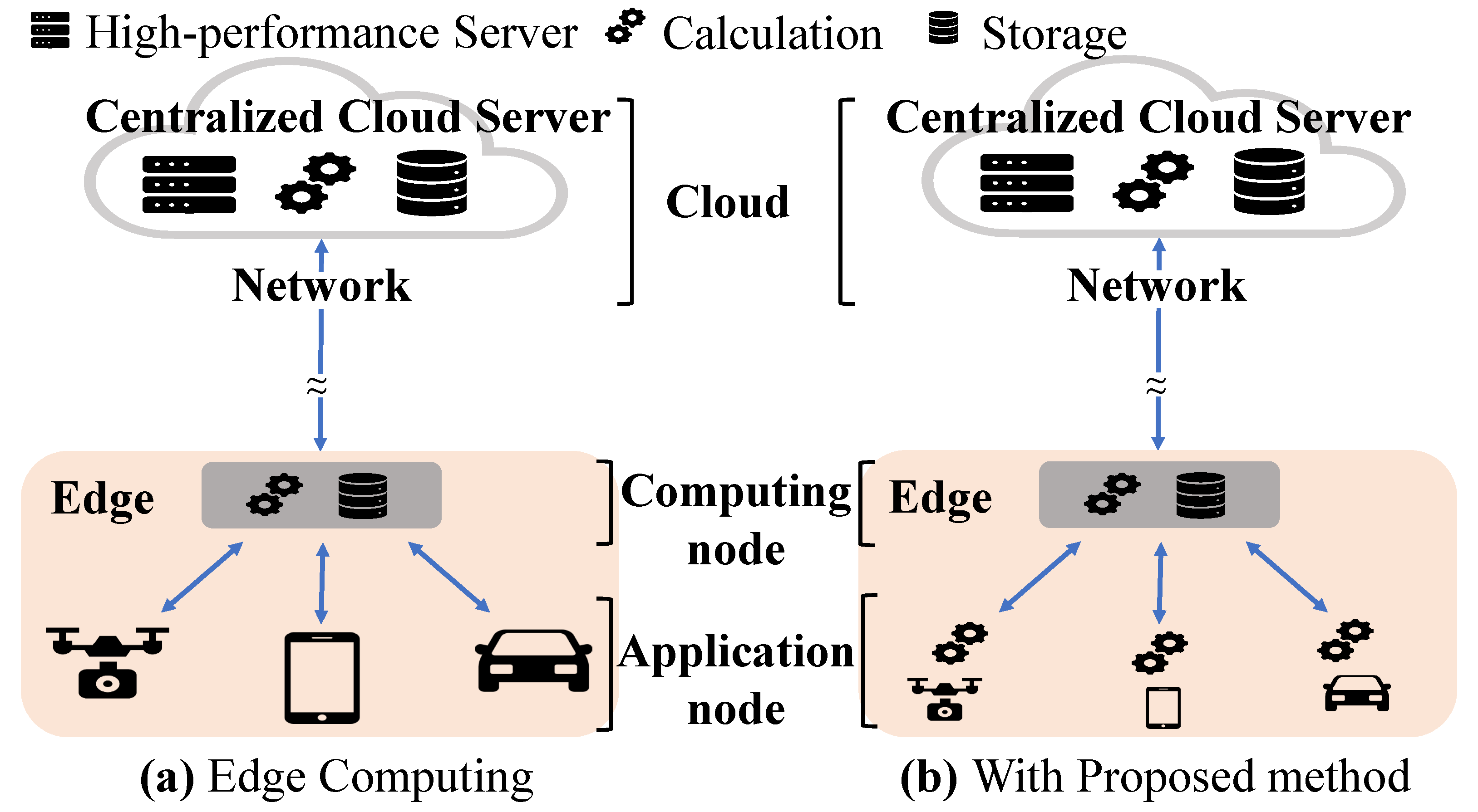
For edge computing, operational systems in the field are typically categorized into application nodes and computing nodes. Illustrated in Figure 1a, the conventional edge computing setup involves an application node responsible for data collection and transmission to the computing node. Subsequently, the computing node handles urgent data processing requests from the collected data, returning results to respective application nodes. Data that necessitate more intricate calculations but lack urgency are routed to the cloud server.

Figure 1.
Comparison of the edge computing.
When the number of application nodes is extensive, the volume of collected and transmitted data escalates significantly. Consequently, the responsiveness of the computing node in the field diminishes due to the burden of transmission and computation [7]. Various strategies have been proposed to alleviate the data load at the computing node. One approach involves training a learning model or implementing data patterns based on previously gathered data. These methods compare the collected data with future data sets, enabling the identification and removal of redundant or irrelevant data. Despite their effectiveness in reducing data processing requirements, these training or patterning techniques still rely on computation at the computing node. Thus, as the number of applications increases, the computational burden on the computing node persists. Addressing this challenge necessitates a reduction in the volume of data transmitted to the computing node, providing a fundamental solution to the computational burden issue.
One potential approach is to delegate some of the computational burden that would typically be performed at the computing node to the application node. Figure 1b depicts the proposed system architecture in edge computing. Here, the collected data undergo preprocessing directly at the application node. This preprocessing may involve tasks such as noise filtering or data reduction, aimed at removing irrelevant or redundant data. Following preprocessing, the refined data are then transmitted to the computing node. Consequently, not only are the data streamlined before transmission, but the burden on data transmission is also alleviated. A micro-controller unit (MCU) is applied to edge computing as application nodes typically because it includes all principle elements as a computer such as the processing unit, memory, ADC, and power supply in a chip. When transferring a portion of the computing node’s workload to the application node, the primary concern arises from the energy consumption incurred by the preprocessing. Typically, application nodes are designed with a focus on data collection and transmission, characterized by small form factors and minimal battery size. Consequently, increasing battery consumption due to preprocessing could render the application node incapable of fulfilling its original tasks. Therefore, rather than just allocating the preprocessing workload to the MCU core, it is required to preprocess effectively using a new IP. In particular, the preprocessing should operate with low power considering application nodes that are sensitive to power consumption because they must generally operate on batteries.
To address this energy issue, this paper proposes the design of customized IP specifically tailored for preprocessing. By allowing collected data to pass through the preprocessing system directly, without the need for additional core-based computations via a high-performance bus, the application node can execute preprocessing tasks with minimal energy consumption. In this paper, rather than replacing the core, we proposed and implemented an IP specialized for data collection and processing as a side-kick along with the core. Then, we verified the performance and area/power consumption. We initially implement the preprocessing system within the FPGA simulation environment, wherein the collected data undergo processing through noise filters and data reduction modules. We analyze the relationship between the data reduction ratio and the extent of signal alteration. Then, the optimal data size considering data corruption is figured out. Subsequently, we synthesize the MCU core and peripherals on the BUS architecture using an open library. Then, we validate the area and power consumption of the preprocessing circuit within the entirety of an MCU system.
We confirm a reduction in data transmission by 50% under 72 of RMSD and 99% data similarity threshold. Additionally, we observe that the area and power consumption of the preprocessing system constitute only 3% and 13% of the entire MCU system, respectively.
The contribution of this paper is summarized as follows:
- the MCU architecture with the preprocessing system is introduced;
- the preprocessing system is implemented as IP modules;
- the trade-off between data reduction and signal corruption is analyzed;
- the complete MCU system is synthesized with an open library, and the size and power of the proposed preprocessing system are evaluated.
The research trend for the edge computing and related concerns are described in Section 2. The proposed preprocessing system for the IoT data collection is introduced in Section 3. The reduction in the data transmission by the preprocessing system are evaluated in Section 4, in which the implementation of the preprocessing in the MCU is discussed. This paper is concluded in Section 5.
2. Related Work
In the wireless IoT network system, the amount of data transmission is the main burden because of the long distance between the computing node and the cloud server. One of the key methods to reduce the transmission data is to send only essential data with efficient data pruning methods. For example, a learning model is trained based on previously collected data. Then, the model is compared with newly collected data to remove meaningless data before sending the data to the computing node. The ratio of the data loss by the removing operation varies by multi-element decision-making algorithms. Depending on the applied models and decision-making algorithms, it is possible to minimize the data loss while sustaining the reduced transmission data.
Unnecessary data are simply identified and removed by analyzing patterns of previously collected data [8,9]. The data reduction algorithm is based on a pattern system consisting of a pattern library and a pattern classifier. The redundant or repetitive data are removed. Another data reduction to remove noise or duplicated data is introduced [10]. This method is performed by data filtering with average values of the previously collected valid data. The data filtering process is feasible in real time if this process is performed in the high-performance computing node. Some studies propose the prediction-based data compensation and compression methods [11,12]. Proposed models predict the future data or missing data between measured time intervals, based on previous collected data with step-size least-mean square algorithm and neural networks. The compensated data are then compressed using various lossless compression methods such as Huffman encoding. All data reduction methods described above are performed on computing nodes. Therefore, the computational burden may become more severe when high-performance algorithms or models are applied.
There are several methods to relieve the burden on computing devices. A way to reduce the computation burden at computing nodes is to control the frequency for the data collection [13]. The frequency is set based on the computational burden at the computing node, the power consumption at the application node, and the number of applications per one computing node. Balancing the computational burden among the computing node is another way. For example, a computing node bypasses a part of receiving data to another computing node if the amount of data is too much [14]. However, they are not fundamental methods to resolve the computational burden at the computing nodes. Rather, they are solutions to allocate a part of the process for reducing transmission data to application nodes such as collecting data without noise nor redundant bits.
Typically, when performing noise filtering and data reduction within an MCU, it is common practice to utilize the MCU’s Arithmetic Logic Unit. Despite the widespread use of this preprocessing for collected data, there is little research on the design of separate IPs for incorporation into MCUs to achieve low power.
3. Preprocessing System
MCU is used in a variety of IoT applications due to its advantage of being easily controllable using programming language. There are various MCU products sold on the market depending on their performance, and the appropriate MCU is selected depending on the field and level of use. Patch size application nodes that collect data by attaching them to humans, animals and plants for health care and smart farms have recently been in the spotlight. In these applications, the devices absolutely require the use of batteries. So, not only high performance but also efficient power management is essential [15]. In response to this demand, low-power and high-performance embedded chips are being released on the market these days. Kontron, a company in the IoT and embedded computing technology field, has launched a single board computer (SBC-EKL) that can perform real-time computing and graphics processing while managing low power [16]. Even though it is able to play a variety of roles as a computing node in edge computing, the chip size is still large, and the power consumption is not low enough to be used as an application node for health care and smart farms.
Therefore, it is necessary to directly design an MCU for an application node that can be attached to something. In addition to simply requiring a small chip size and low power consumption, there is also a need to reduce the amount of data transmission to send data to the computing node. To resolve this complicated problem, we propose a preprocessing system.
3.1. Preprocessing Approach
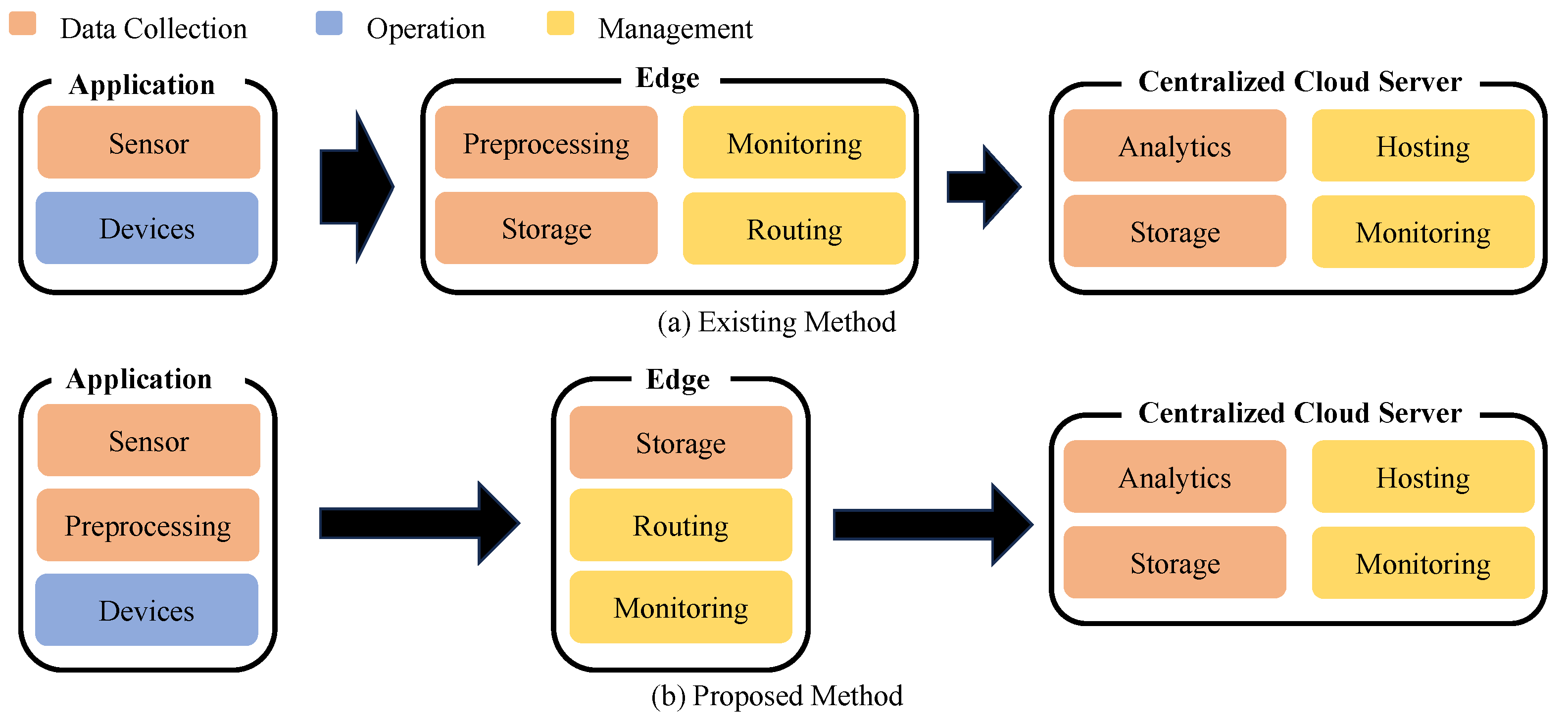
Figure 2 shows the existing and proposed methods for data collection and transmission to the computing node for operations such as analysis and calculation. The existing method transmits large amounts of data collected from applications to computing nodes as shown in Figure 2a. Then, computing nodes perform the operation after data preprocessing. This method places a burden on data transmission from applications to computing nodes. Moreover, computational burden by the preprocessing still remains in the computing node.
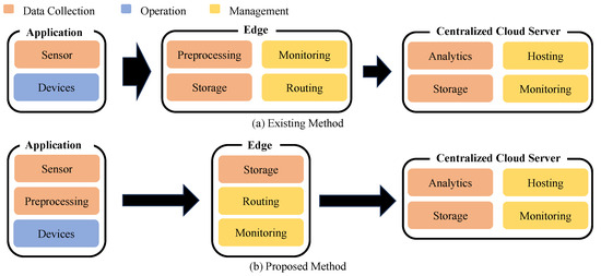
Figure 2.
Method comparison.
Unlike existing edge computing, we propose a system where applications collect data and perform preprocessing as shown in Figure 2b. However, there are some key requirements for the preprocessing in the application:
- operation within the MCU architecture;
- low computing power and system size;
- use of low-power bus for data transfer.;
First, preprocessing is operated within the MCU architecture. As mentioned in Section 1, the application node is made with MCU architecture. If we attach another MCU for the preprocessing, it requires greater system size and power consumption. Second, the preprocessing at the application node should require low computing power consumption and area. If the preprocessing is operated by the core of the MCU, we need a core with higher computing power. In typical, application nodes are attached to mobile devices and collect data with very small power consumption. For example, application nodes are operated with only photovoltaic panels or small-size batteries. Therefore, a purpose-designed processing module should be designed inside of the MCU. Third, data collecting and preprocessing should be performed in low-power bus architecture to satisfy the energy issue at the application node. Otherwise, the battery actually causes limitations in data collection activity. To resolve the above requirements, we suggest a preprocessing approach, which is suitable to the application node.
3.2. Proposed MCU BUS Archtecture
3.2.1. MCU Concept
We design a preprocessing module for data filtering and reducing in the MCU architecture. Figure 3a shows a typical MCU architecture for data collection and transmission. The data are collected by the I/O module and validated with a debug system module. The data are modified as a packet for wireless communication by the core. The packet is transmitted via the peripheral module. Figure 3b shows the MCU architecture for preprocessing. The yellow square is the purpose-designed preprocessing module. This module is used for data reduction, meaningless data removing, data filtering, etc. Therefore, it is possible to modify the collected data as a first step that suits users’ purpose.
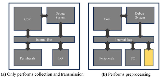
Figure 3.
MCU diagram.
3.2.2. BUS Architecture
Typical Advanced Microprocessor Bus Architecture (AMBA) typically consists of two types of buses: Advanced Peripheral Bus (APB) and Advanced High Performance BUS (AHB). Figure 4 shows the two bus lines. APB is designed for connectivity to the peripherals such as communications. The operation is simple and requires relatively low power consumption. AHB is for high-speed interconnection to the memory or processor, which is marked blue in Figure 4. For the high data transmission, the AHB controller (AHB CTRL) includes multiplexers for several signal senders (masters) and receivers (slave) and an arbiter for managing the multiplexers. There is an AHB/APB bridge between AHB and APB to exchange the data. Due to this bridge, the data from outside are stored into the memory and manipulated by the processor.
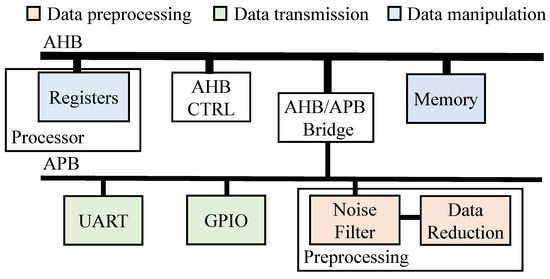
Figure 4.
Proposed BUS architecture.
When multiple masters need to use the same bus in AMBA, the arbiter mediates the order of the usage of the bus with the round robin method or fixed priority method. The round robin method allows each master to access the bus in order, and the fixed priority method allows the master with the highest priority to access the bus first.
Sending and receiving data through the bus is controlled by the handshaking method. When the master requests the arbiter to use the bus, and the arbiter grants the master permission to use the bus through above arbitration methods. The master then sends a signal to the slave to check whether the slave is ready to send or receive data. Once confirmation is complete, data are transferred through the BUS.
3.2.3. AMBA as Application Nodes
The main role of the IoT application nodes is to collect the key data from environment. Then, the data are stored in the memory or sent to the computing node with wireless communication. The collected data are entered to the AMBA by general-purpose input and output (GPIO). Many kinds of serial communication protocols such as UART, SPI and are used with GPIO. The peripherals for the data communication is marked green in Figure 4. The data are sent to the memory on the AHB through AHB/APB bridge. Then, the data can be manipulated by the processor or are sent to the outside by GPIO or UART.
However, from the energy perspective, most application systems are operated with battery. So, low-power operation is one of the most important concerns for the application sensor nodes. Therefore, it is better to use low-power APB peripherals for the data manipulation rather than use the high-speed processor on the AHB.
3.2.4. Preprocessing Modules
The red modules in Figure 4 show the preprocessing modules: noise filter and data reduction. For the low-power operation, the modules are attached on the APB. The preprocessing consists of two steps: (1) noise filtering and (2) data reduction or compression. When collected data come in through GPIO, the data are sent to the filter module to remove noise or meaningless data. There are various noise filter circuits in the academia and industry. But, in this paper, we only discuss digital filters such as the digital low-pass filter. The operation requires low energy compared with operation in the processor unit.
Then, the data reduction process is designed to reduce the size of the data for the wireless transmission. Because of the limitation of the lossless data compression, lossy compression can be an option for the wireless data transmission. Thanks to the sufficiently advanced filters and compression methods, the information lost during the preprocessing is not that large. On the other hands, the amount of data for the transmission is directly related to the traffic and workload to the computing node.
3.3. Preprocessing Operation
Figure 5 illustrates the preprocessing operations comparing conventional and proposed processes, with architectures depicted in a simplified manner from Figure 4.
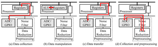
Figure 5.
Conventional preprocessing operation via AHB and APB (a–c) and proposed preprocessing operation via APB only (d).
In the conventional preprocessing workflow (Figure 5a–c), the initial step involves storing the collected data, received from the analog–digital converter (ADC), in registers via the AHB/APB bridge. Subsequently (Figure 5b), the processor unit manipulates the data to execute preprocessing tasks such as noise filtering and data reduction using typical instruction-based operations. Finally (Figure 5c), the processed data are transmitted via GPIO. However, this conventional approach often results in significant energy consumption due to the involvement of the processor in data preprocessing.
In contrast, the proposed preprocessing system (Figure 5d) transfers collected data directly to preprocessing modules, enclosed within a dashed box. After undergoing filtering and reduction, the processed data are then forwarded to GPIO or a buffer for transmission. Notably, all preprocessing tasks are executed by IP-based operations through APB, requiring low-speed but low-power consumption since the processor unit remains uninvolved in these operations. The detailed implementation of the noise filtering and data reduction are explained in Section 4.1.2 and Section 4.1.1, respectively. The power and area consumption of the preprocessing modules are estimated in Table 1 and Table 2.

Table 1.
Area of modules in AMBA.
Table 2.
Power of modules in AMBA.
The proposed preprocessing modules are connected to the APB as a slave, and the data collected from GPIO are transmitted to the preprocessing module in accordance with the handshaking signal. The preprocessing result through the noise filter and data reduction can eventually be delivered to another IP according to the handshaking signal.
4. Evaluation
We evaluate preprocessing from two perspectives. The first is the amount of the data reduction and related information loss by the preprocessing in Section 4.1. The validation is performed with the RTL simulation using open experimental data. The second is the area and power consumption of the preprocessing module in the practical application node in Section 4.3. The preprocessing is implemented with the AMBA structure where the LEON3 core and IPs for AHB/APB control and test are designed by the MCU open library.
4.1. Evaluation Setup
We adopt a case study where the application node uses the electrocardiogram (ECG) sensor to collect biological data. The peak amplitude of the ECG waveforms is in millivolts (mV), which is easily affected by noise during the measurement. Therefore, it is difficult to analyze the patient’s symptoms if the noise is mixed with the ECG waveform. It is mandatory to use an efficient data filter to remove the noise components.
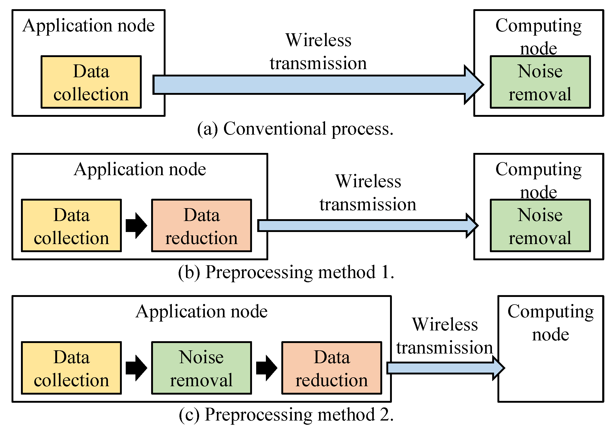
Figure 6 shows the scenarios in the case study that include the proposed preprocessing system. Figure 6a shows the conventional IoT system. The collected data are sent to the computing node without data reduction. Therefore, the amount of wireless transmission is relatively large. The process of noise removal is performed in computing node, and the result is stored in a memory to prepare transmission to the cloud server. Figure 6b shows preprocessing method 1 that performs the data reduction in the application node to alleviate wireless transmission volume. The noise removal process in the computing node is following the transmission. Preprocessing method 2 in Figure 6c includes data collection, noise removal and data reduction in the application node. After all preprocessing, the result is sent to the computing node. In this case, there is nothing to do in the computing node for data manipulation.
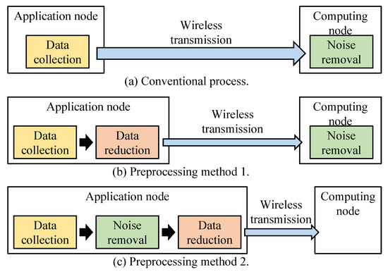
Figure 6.
Case study scenarios to validate the preprocessing system.
4.1.1. Data Reduction
The data reduction is performed by just removing lower bits to reduce the amount of transmission. For example, an 8-bit binary datum 01110 1101 is sent as higher 6-bit 0110 11. Then, lower bits are filled with zeros such as 0110 1100. As more data are reduced, the transmission burden decreases, while more information will be lost. If the data are reduced before the noise removal process, the proportion of the noise among total information will be increased.
4.1.2. Noise Removal
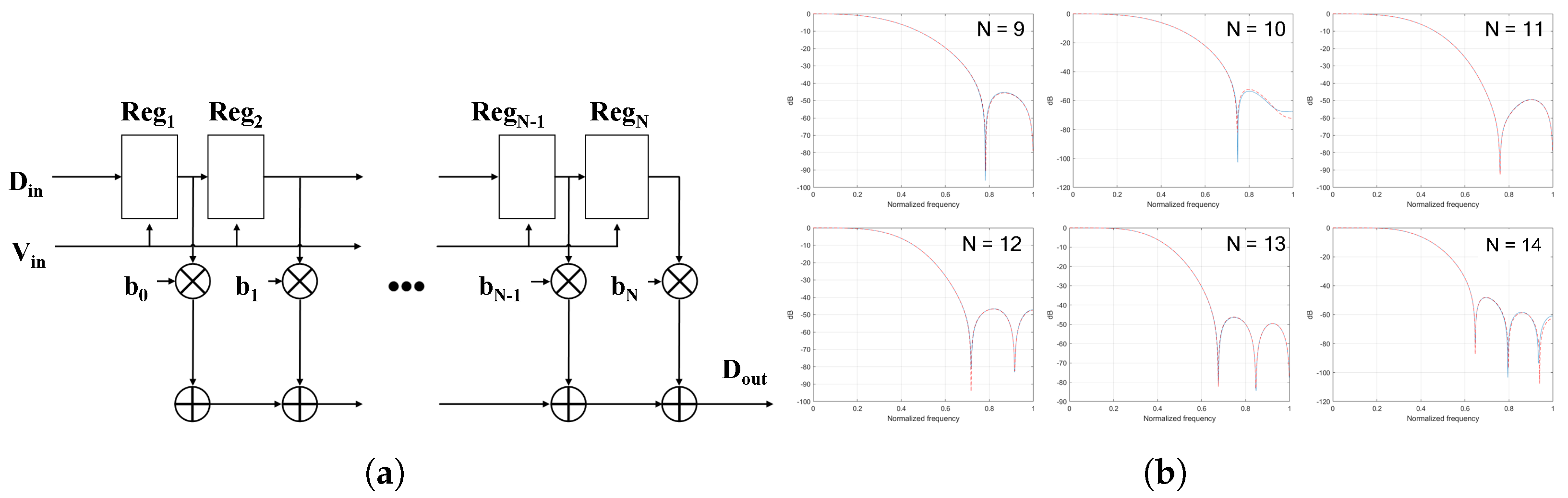
We implement the Finite Impulse Response (FIR) filter for the noise removal process. FIR filter is a typical low-pass filter whose impulse response is of finite duration. Figure 7a shows the structure of the FIR filter in which N registers, N multipliers, and N adders are included. As N increases, the accuracy of the frequency response is enhanced as Figure 7b that shows the frequency response by N.
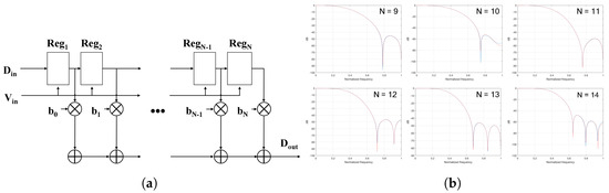
Figure 7.
Implementation of the FIR filter. (a) The structure of FIR filter; (b) The frequency response.
The performance of the FIR filter is determined through Matlab simulation as shown in Figure 7b. Once the coefficient is confirmed for a given application, the circuit is designed accordingly. In the ECG-based experiment, 14 registers are used, and the results are shown in Section 4.2.
4.1.3. Test Environment
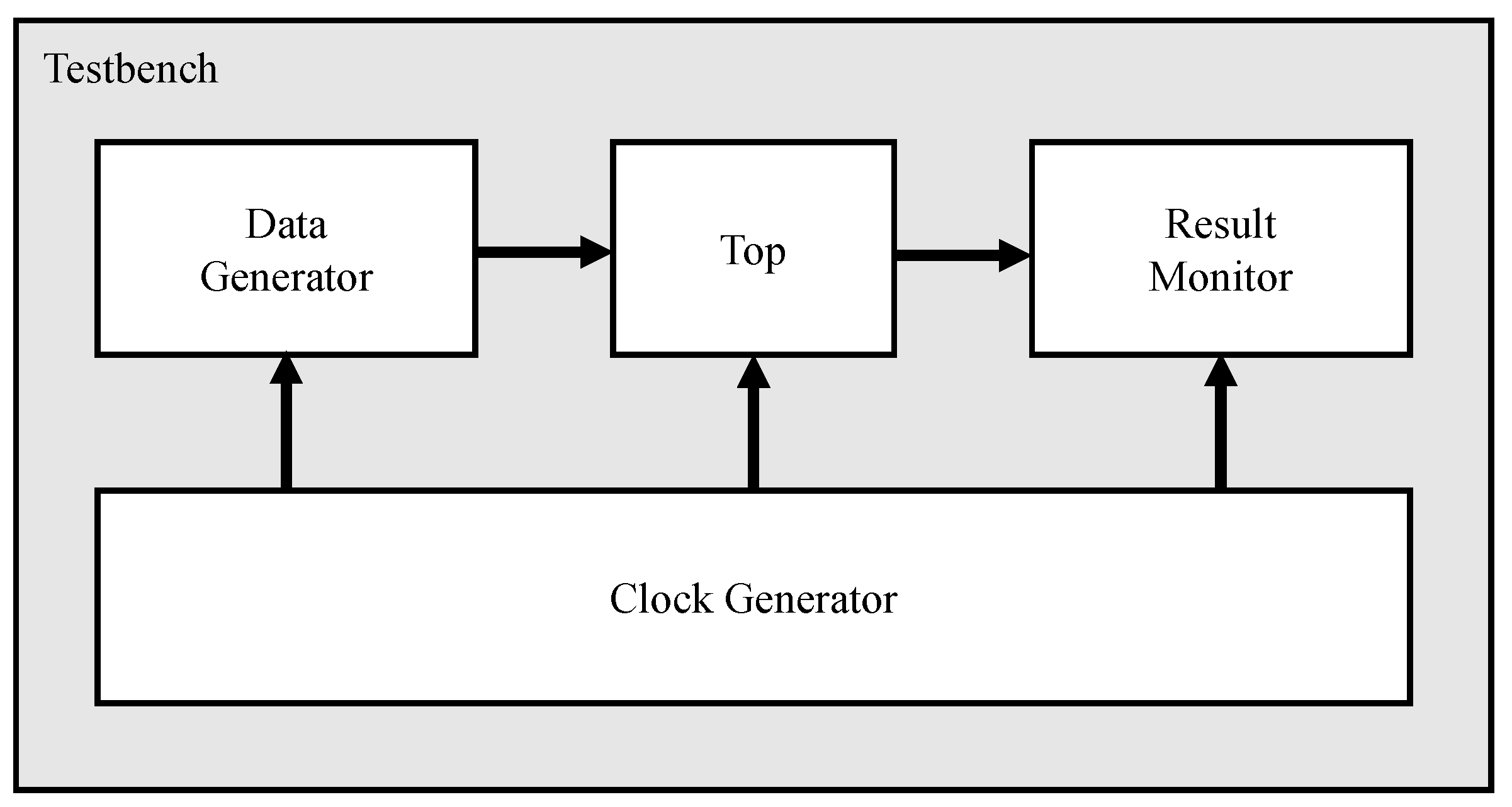
We evaluated the operation in the test environment in Figure 8. The environment is designed with RTL codes using Verilog language. Data generator works like a data collector in Figure 6 that reads the ECG measurement data and sends them to the top module. Top includes data reduction and noise removal modules. The results after the data reduction and noise removal is stored in Result Monitor where the similarity of the preprocessing is performed compared with the conventional process that uses only noise removal.
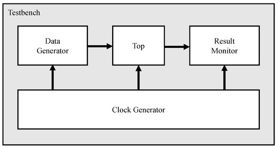
Figure 8.
Test environment.
We use two metrics to evaluate the similarity of the preprocessing results: Root Mean Square Deviation (RMSD) and cosine similarity. RMSD is often used to deal with differences between predicted value and reference value. This metric is used widely to compare the magnitude between two data. The formula is as follows:
where and y are the reference data without data reduction (conventional process) and preprocessing data (method 1 and 2). T means the number of data.
Cosine similarity refers to the similarity between two vectors using the cosine angle without the consideration of signal magnitude. If the directions of the two vectors are exactly the same, the value is 1, and if the directions are opposite, the value is −1. We can check the impact of the noise on the signal.
4.2. Performance Evaluation
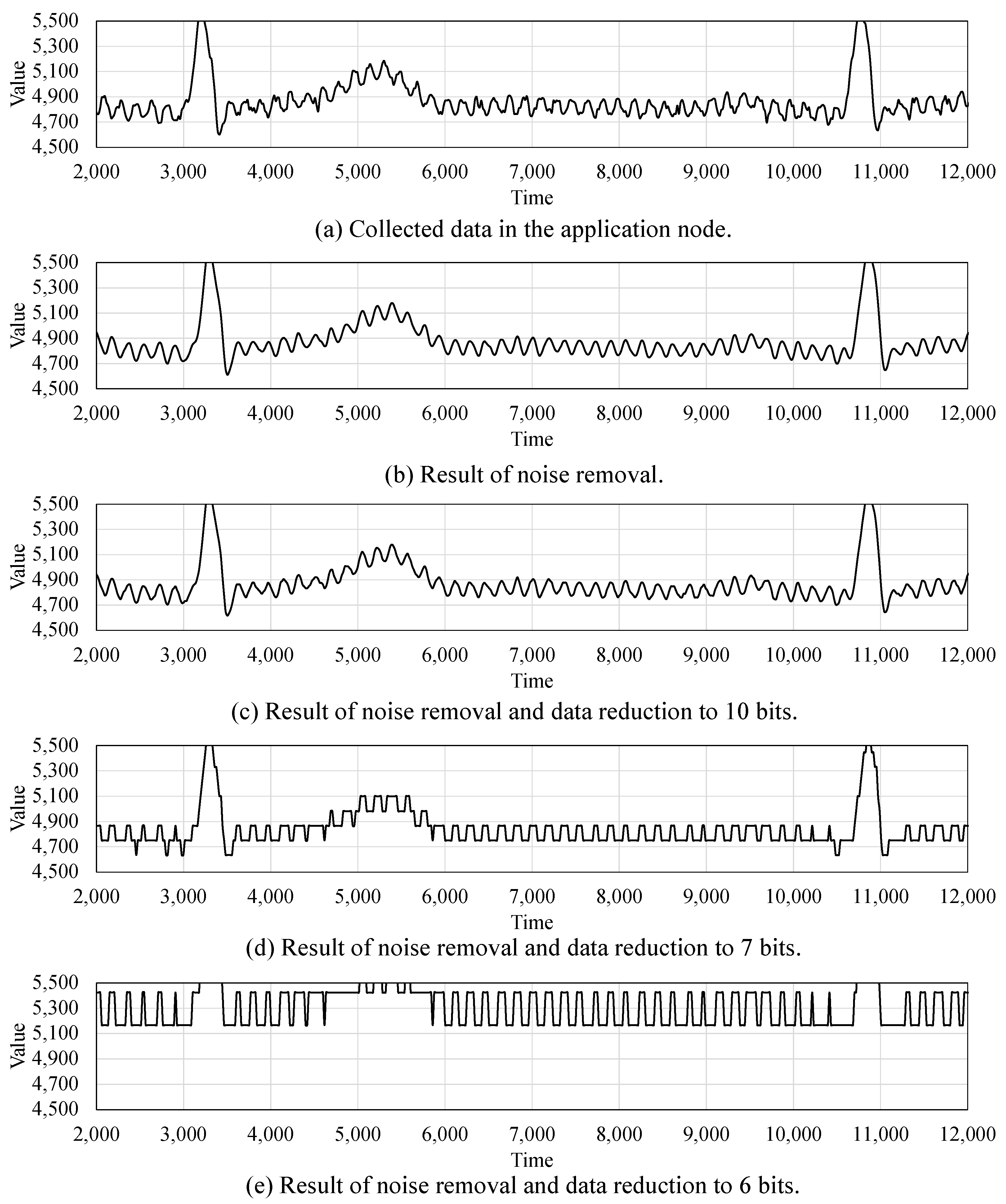
Figure 9 shows the evaluation results of noise removal and data reduction on the 14-bit ECG data. Figure 9a shows the collected data in the application node, which includes the noise term. The results of the noise removal are shown in Figure 9b. Distorted values in Figure 9a are not visible in the result graph. Figure 9c–e are the graphs after data reduction from 14 bits to 10 bits, 7 bits and 6 bits, respectively.
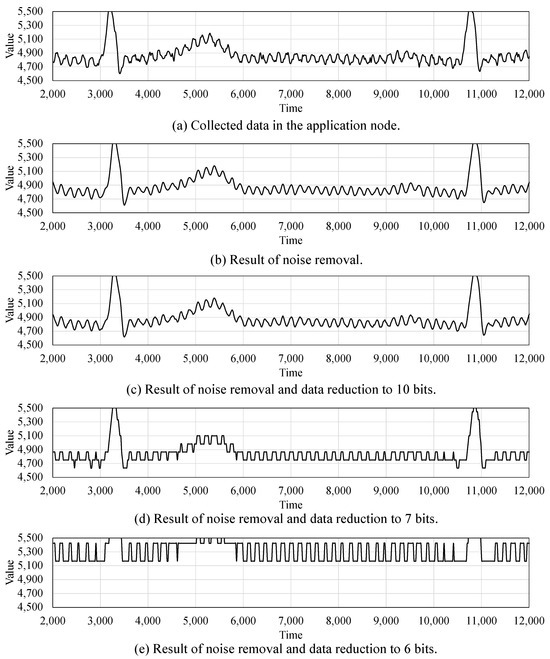
Figure 9.
Data collection (a), noise removal (b) and data reduction results (c–e).
When the data are reduced to 10 bits, signal distortion due to data reduction is almost invisible. However, in the case of the data reduction to 7 bits, there is quite a lot of signal distortion. Finally, in Figure 9e, the amplitude of data is shifted significantly, and the data cannot be restored. As 1 bit of data is reduced, the range of numbers that can be expressed is reduced by half. Therefore, reducing the data size causes significant signal distortion after a certain point.
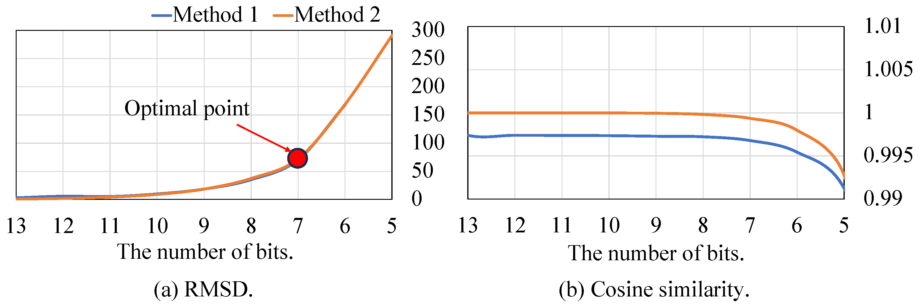
Figure 10 summarizes the preprocessing results in terms of two different costs RMSD and cosine similarity. The blue line means preprocessing method 1 (data reduction → noise removal), and the orange line means method 2 (noise removal → data reduction). Metric RMSD mainly shows the signal distortion based on the amplitude difference. In Figure 10a, in the case of over 10 bits, there is almost no signal distortion because it is possible to cover the signal information with 10 bits. As the number of available bits is decreased lower than 7 bits, the information lost increases sharply. As we see in Figure 9, 7 bits is almost the minimum size for utilizing the information. If the amount of data is reduced further, the amount of transmission will of course be reduced, but it cannot be utilized in computing nodes. In addition, there is little difference between results from method 1 and 2.

Figure 10.
Comparison between the results of method 1 and method 2 in two metrics.
In the metric cosine similarity in Figure 10b, cosine similarity shows less distortion even when the data are reduced less than 6 bits. The main reason is that cosine similarity does not care about signal magnitude and only considers the frequency of the data. In the comparison between two methods, method 2 is better than method 1 with respect to the most number of bits. In the case of method 2, there is no factor causing signal distortion if the number of bits is enough. On the other hand, in method 1, the data reduction is performed while including noise. Therefore, the proportion of the noise among total information is increased, which causes relatively lower cosine similarity.
In summary, if the amount of data is reduced to a certain level (less than 7 bits in this case study), the communication burden can be greatly reduced without information loss. The amount of data transmission is reduced by 50% under acceptable information loss: 72.07 of RMSD and 0.99937 of cosine similarity.
4.3. Area and Power Evaluation
In this section, we validate the area and power consumption of the proposed preprocessing system in an MCU. Therefore, it is mandatory to implement MCU operating under AMBA. We first implement MCU with the open MCU library and attach our preprocessing system to the AMBA. Then, we evaluate the proportion of the preprocessing system in terms of area and power consumption.
4.3.1. MCU Implementation
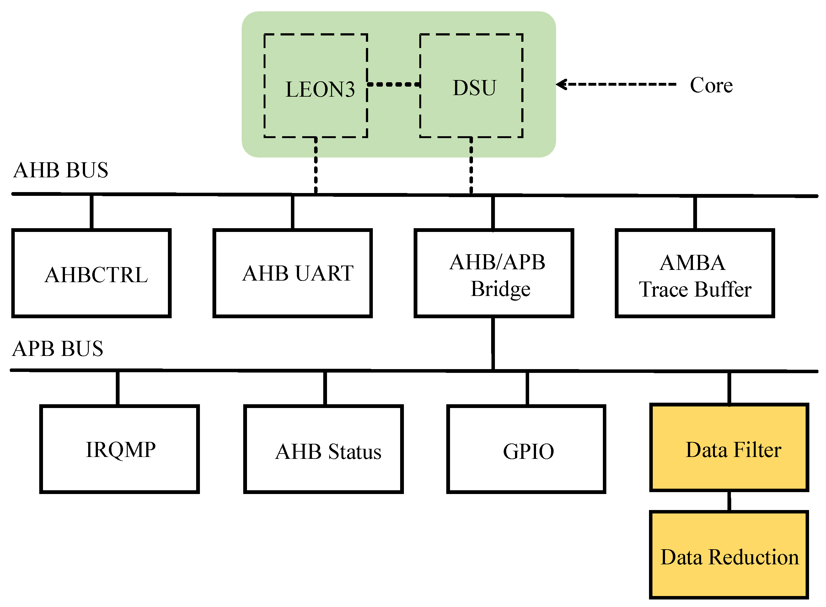
For the MCU implementation, we use the LEON 3 Processor provided by Gaisler to configure and connect the desired IPs based on GRLIB, an open MCU library, that includes the LEON core, debug support unit (DSU), bus controller, AHB/APB bridge and related monitoring modules [17]. Figure 11 shows the implementation of AMBA with GRLIB. The preprocessing modules, the noise filter and data reduction, are attached to the APB bus. The MCU core, LEON3 and DSU, is connected to the AHB bus. Data flow through AMBA is operated through the control of the core.

Figure 11.
AMBA with GRLIB.
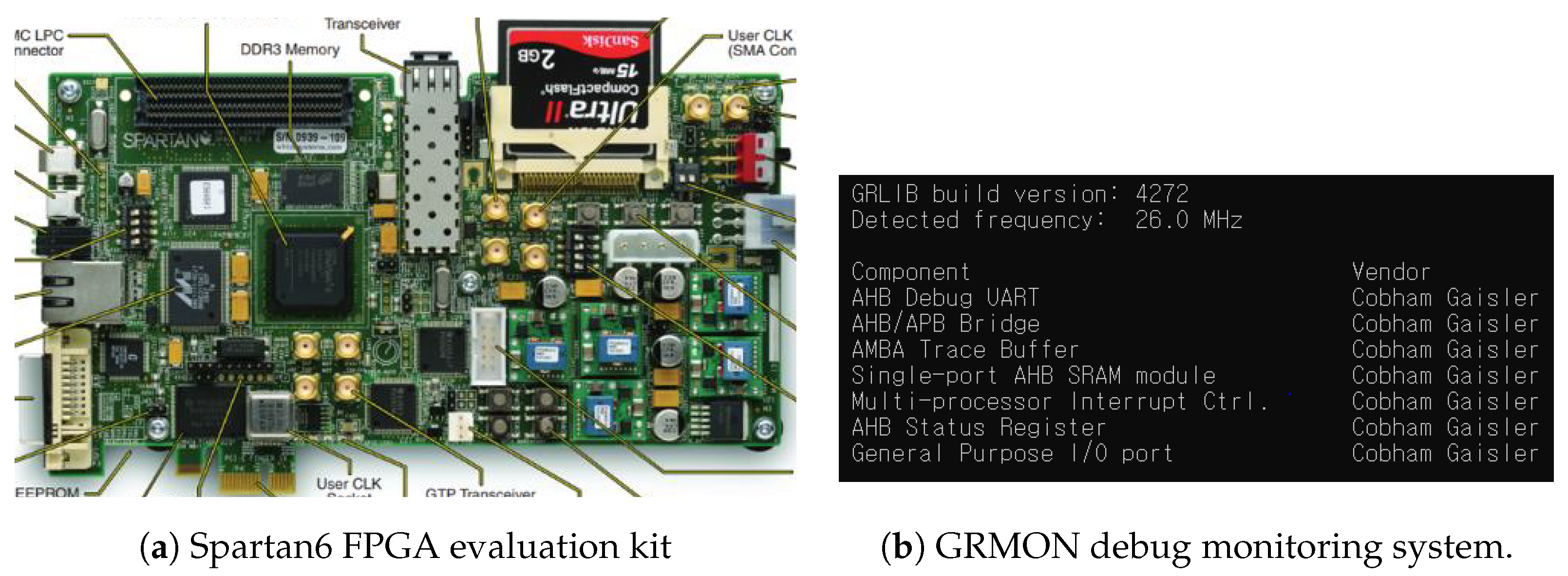
We implement the MCU as VHDL and synthesize it to operate on the Xilinx FPGA board. Figure 12a shows the Spartan6 FPGA evaluation kit where the LEON 3 processor and IPs from GRLIB are implemented. We connect the board to the PC through UART communication to check whether IPs connected to AMBA work properly using GRMON.
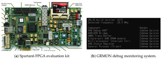
Figure 12.
MCU implementation.
GRMON is a debug monitor designed to debug AMBA based on LEON or NOEL processors. GRMON is connected to the dedicated LEON 3 debug interface, which allows you to read or write various register values within the IO port module via AHB or APB. GRMON checks whether the modules implemented and operated on the AMBA configuration are properly connected to the bus. Figure 12b shows the debug monitoring results showing on the PC monitor. Using GRMON, it is possible to check most IPs connected to AMBA. We confirmed the proper operation of modules on AMBA.
4.3.2. System Evaluation
In order to apply the proposed preprocessing to the MCU for the application node, its size and power consumption should be sufficiently small. For the evaluation of the area and power consumption, we synthesize the MCU VHDL codes for Application-Specific Integrated Circuit (ASIC). We use the Design Compiler of Synopsys [18] and process design kit (PDK) from DB hitek 180 nm technology [19]. The target clock frequency in this synthesis is 84 Mhz. The following Table 1 and Table 2 show the size and power consumption of the preprocessing system among the MCU IPs including LEON3 core. Among the AMBA structures, the preprocessing system occupies only 3.6%, which is sufficiently small. Also, the power consumption is 13.1%, which is little larger than other modules for AMBA. However, we confirmed that the difference is not large because the modules in the Table 2 are only for essential control modules in AMBA. If frequently used IPs are connected to the AMBA, the portion of the preprocessing may be shrunken.
We evaluate the overall power consumption of preprocessing operations with the MCU core and proposed modules. We choose ATmega328 [20], which is a well-known MCU for IoT devices such as Aduino Uno [21]. ATmega328 has various power-saving modes where some modules consuming a lot of power are turned off. Table 3 shows three different power-saving modes and their power consumption. We referred the power consumption in each mode from the datasheet by assuming that the operating frequency is 1 Mhz, operating power is 1.8 V, and temperature is 25 Celsius degree. All devices are working in the active mode, and only the MCU core is turned off under the idle mode. If the system enters the standby mode, most systems, except the main clock (OSC) and interrupts (INT), are turned off. As we know, the MCU core consumes most of the power consumption. We also attached the power consumption of the proposed preprocessing modules based on Table 2, which is scaled down according to the given operating conditions. If the preprocessing is performed only with MCU core, it consumes 360 μW. While if we use preprocessing modules under the idle mode, the overall power consumption is expected to be 92 μW, which means the power consumption is reduced to 74.4%.
Table 3.
Power consumption in different power saving modes of the commercial MCU and scaled power consumption of the preprocessing modules.
5. Conclusions
To alleviate transmission burden on edge computing, we introduce the preprocessing system for MCU to reduce the transmission data with low power consumption. We find the optimal data size to reduce the transmission data as much as possible while preserving the signal integrity. To evaluate the preprocessing system, we design and implement the preprocessing system and MCU system via hardware description language on an FPGA. Also, we synthesize the MCU system to estimate the size and power consumption of the preprocessing system. As the field of use of IoT application expands, the demand to reduce battery consumption when collecting data will steadily increase. In particular, when designing an MCU for data collection and transmission, this preprocessing system is expected to be widely applied to the methodology to reduce the amount of data transmission with low power consumption. Also, as a future work, IoT for autonomous vehicles is a promising area. Naturally, in an autonomous vehicle environment, stable power can be supplied to the sensor node, and data communication is also carried out by wire. In this environment, it is necessary to design considering performance and high bandwidth so that sufficiently accurate values can be transmitted in real time rather than low power.
Author Contributions
Conceptualization, C.R. and D.B.; methodology, C.R. and D.B.; validation, D.K. and C.R.; writing—original draft preparation, D.K., C.R. and D.B.; writing—review and editing, D.K., S.-g.C. and D.B.; supervision, D.B. All authors have read and agreed to the published version of the manuscript.
Funding
This research was supported by Chungbuk National University Korea National University Development Project (2023).
Data Availability Statement
The data are not publicly available by the school of Semiconductor Engineering.
Conflicts of Interest
Author Chanhwi Roh was employed by the company ABOV Semiconductor Co., Ltd. The remaining authors declare that the research was conducted in the absence of any commercial or financial relationships that could be construed as a potential conflict of interest.
References
- Computing, F. Fog computing and the Internet of Things: Extend the Cloud to Where the Things are. Cisco White Pap. 2015, 13, 1–6. [Google Scholar]
- FutureScape IDC. Worldwide Internet of Things 2017 Predictions; IDC Research, Inc.: Framingham, MA, USA, 2016. [Google Scholar]
- Varghese, B.; Buyya, R. Next generation cloud computing: New trends and research directions. Future Gener. Comput. Syst. 2018, 79, 849–861. [Google Scholar] [CrossRef]
- Wu, Y.; Jiang, H.; Ma, Z.; Gou, P.; Lu, Y.; Han, J.; Yin, S.; Wei, S.; Liu, L. An Energy-Efficient Approximate Divider Based on Logarithmic Conversion and Piecewise Constant Approximation. IEEE Trans. Circuits Syst. I Regul. Pap. 2022, 69, 2655–2668. [Google Scholar] [CrossRef]
- Di Meo, G.; Saggese, G.; Strollo, A.G.M.; De Caro, D.; Petra, N. Approximate Floating-Point Multiplier based on Static Segmentation. Electronics 2022, 11, 3005. [Google Scholar] [CrossRef]
- Capra, M.; Peloso, R.; Masera, G.; Ruo Roch, M.; Martina, M. Edge Computing: A Survey on the Hardware Requirements in the Internet of Things World. Future Internet 2019, 11, 100. [Google Scholar] [CrossRef]
- Varghese, B.; Wang, N.; Barbhuiya, S.; Kilpatrick, P.; Nikolopoulos, D.S. Challenges and Opportunities in Edge Computing. In Proceedings of the 2016 IEEE International Conference on Smart Cloud (SmartCloud), New York, NY, USA, 18–20 November 2016; pp. 20–26. [Google Scholar] [CrossRef]
- Larrakoetxea, N.G.; Astobiza, J.E.; López, I.P.; Urquijo, B.S.; Barruetabeńa, J.G.; Rego, A.Z. Efficient Machine Learning on Edge Computing Through Data Compression Techniques. IEEE Access 2023, 11, 31676–31685. [Google Scholar] [CrossRef]
- Idrees, A.K.; Jaoude, C.A.; Al-Qurabat, A.K.M. Data Reduction and Cleaning Approach for Energy-saving in Wireless Sensors Networks of IoT. In Proceedings of the 2020 16th International Conference on Wireless and Mobile Computing, Networking and Communications (WiMob), Thessaloniki, Greece, 12–14 October 2020; pp. 1–6. [Google Scholar] [CrossRef]
- Chen, A.; Liu, F.H.; Wang, S.D. Data Reduction for real-time bridge vibration data on Edge. In Proceedings of the 2019 IEEE International Conference on Data Science and Advanced Analytics (DSAA), Washington, DC, USA, 5–8 October 2019; pp. 602–603. [Google Scholar] [CrossRef]
- Hussein, A.M.; Idrees, A.K.; Couturier, R. Distributed energy-efficient data reduction approach based on prediction and compression to reduce data transmission in IoT networks. IEEE Trans. Veh. Technol. 2022, 35, e5282. [Google Scholar] [CrossRef]
- Jarwan, A.; Sabbah, A.; Ibnkahla, M. Data Transmission Reduction Schemes in WSNs for Efficient IoT Systems. IEEE J. Sel. Areas Commun. 2019, 37, 1307–1324. [Google Scholar] [CrossRef]
- Suryavansh, S.; Benna, A.; Guest, C.; Chaterji, S. A data-driven approach to increasing the lifetime of IoT sensor nodes. Sci. Rep. 2021, 11, 22459. [Google Scholar] [CrossRef] [PubMed]
- Zhang, J.; Guo, H.; Liu, J.; Zhang, Y. Task Offloading in Vehicular Edge Computing Networks: A Load-Balancing Solution. IEEE Trans. Veh. Technol. 2020, 69, 2092–2104. [Google Scholar] [CrossRef]
- The Building Blocks of Edge Computing. Available online: https://www.eetimes.eu/the-building-blocks-of-edge-computing/ (accessed on 24 July 2024).
- Products of Kontron. Available online: https://www.kontron.com/en/products/boards-standard-form-factors/single-board-computer/3.5-/c164338 (accessed on 24 July 2024).
- GRLIB VHDL IP Library. Available online: https://www.gaisler.com (accessed on 24 July 2024).
- Design Compiler. Available online: https://www.synopsys.com/implementation-and-signoff/rtl-synthesis-test/dc-ultra.html (accessed on 24 July 2024).
- DB Hitek Foundry Service. Available online: https://dbhitek.com/eng/ (accessed on 24 July 2024).
- Microchip Technology Inc. megaAVR Data Sheet; Microchip Technology Inc.: Chandler, AZ, USA, 2020. [Google Scholar]
- Arduino Main Page. Available online: https://www.arduino.cc (accessed on 24 July 2024).


Disclaimer/Publisher’s Note: The statements, opinions and data contained in all publications are solely those of the individual author(s) and contributor(s) and not of MDPI and/or the editor(s). MDPI and/or the editor(s) disclaim responsibility for any injury to people or property resulting from any ideas, methods, instructions or products referred to in the content. |
© 2024 by the authors. Licensee MDPI, Basel, Switzerland. This article is an open access article distributed under the terms and conditions of the Creative Commons Attribution (CC BY) license (https://creativecommons.org/licenses/by/4.0/).