Abstract
The main objective of the work is to investigate the capacity of a single magnetoresistance (MR) element to measure AC electrical currents. An instrumentation system is presented to characterize individually the four active elements of an MR bridge current sensor preserving their internal connections. The system suggests the possibility to sense electrical currents using only one element of the bridge opening the way to design new MR sensors based on this concept. Sensitivity, offset and non-linearity deviation were obtained using bridges of tunnel (TMR)- and giant (GMR)-based MR technologies. The single element embedded in a Wheatstone bridge configuration is used for practical current measurements in a 50 Hz line. An electronic circuitry is proposed to measure alternating (AC) currents with a single MR element, including a lock-in amplifier and an interface to properly convert the signal to its root mean square (rms) value with a resolution of 250 mA peak in the 125 A range.
1. Introduction
Magnetoresistance (MR) technology is used to implement electrical current sensors for a wide range of scientific and industrial applications. This sensing technology has applications in various fields, including material inspection [,], industry [,,], medical monitoring [] and smart grid management [], among others.
For current sensing, manufacturers provide MR sensors arranged in a Wheatstone bridge structure. Currently, for this application, tunnel magnetoresistance technology (TMR) is the preferred MR technology, offering a higher percentage variation in resistance (up to 200% at room temperature) compared to previous MR technologies [,,,].
Magnetoresistance effects, well known in magnetic multilayers, have enabled the micro-fabrication of current sensors, either in a commercial package [,,] or for research purposes [,]. In both cases, the sensor is fabricated by combining four MR elements in a Wheatstone bridge configuration. Once implemented, knowledge of the MR variation in each element becomes particularly important. In a quality control process, an excessive mismatch of the resistance between elements at zero current will determine whether the sensor passes or fails. Furthermore, if a substantial difference of this resistance exists, a high offset voltage at the output of the bridge will be generated and it will decrease the common-mode signal rejection of the whole electronic measurement chain. On the other hand, a mismatch in current sensitivity between elements will cause non-linearity in the nominal sensitivity of the bridge.
In this work, the individual characterization of each of the four MR elements in an MR sensor with a Wheatstone bridge configuration will be one of the main objectives. A complete instrumentation system will be designed to individually characterize each of these four MR elements, providing basic parameters such as linearity, sensitivity and offset, while preserving the internal connections and integrity of the bridge. Experimental results will be obtained for the elements of both industrial and custom-designed MR bridges. Three MR technologies have been considered: TMR, giant magnetoresistance (GMR) and spin-valve (SV) technology. Moreover, sensors in different current ranges will be analysed (medium and high current).
The individual analysis of each of the MR elements of the bridge leads us to explore the application of a single MR element for current sensing. Using a single element instead of a Wheatstone bridge will reduce the steps needed in the microelectronic fabrication process, simplifying layout complexities. The sensor bridge requires a symmetrical variation in resistance between its four elements. This issue does not appear when using a single sensor element. In [], the concept of MR shunt was presented and the temperature coefficients of several MR elements (embedded in a bridge and independent) were obtained. Subsequently, a thermal compensation was proposed for both cases, measuring DC current. However, no AC current measurement development was described.
The use of a single resistive sensing element to measure some physical variable has been used successfully in applications such as temperature and pressure [,,,,]. Temperature can be detected by a constant current biasing a platinum resistance detector to monitor junction temperatures in power modules [] or for accurate measurements in industrial installations []. In [], individual electronic processing is carried out for each of the eight piezoresistive elements distributed in a diaphragm for pressure measurement.
In [], a single piezoresistive element is proposed for pressure measurement under harsh environments. In [], a single piezoresistive element is used for pressure measurement reducing the manufactured microelectronic area. However, the application of an MR element in an AC electrical current measurement has not yet been explored.
The lock-in amplifier is an electronic processing tool that offers high rejection of interferences, time drifts and offsets produced in the measurement chain [,]. It is particularly recommended when measuring weak signals immersed in a high-level noisy electronic environment [,,]. The modulation/demodulation function in a lock-in amplifier ensures that only frequencies very close to the carrier frequency can affect the measured signal. In this way, high signal-to-noise ratios are achieved [,,,].
The single element embedded in a Wheatstone bridge configuration is used in this paper for practical current measurement in a 50 Hz line. An electronic circuitry is proposed to measure AC currents with a single MR element, including a lock-in amplifier and an electronic interface to properly convert the signal to its root mean square (rms) value obtaining a resolution of 250 mA peak in the 125 A range.
This paper is organized as follows. Section 2 presents the instrumentation system designed to individually characterize each of the four elements in a Wheatstone bridge sensor providing its basic parameters (linearity, sensitivity, offset, among others), while preserving the internal connections and integrity of the bridge. Experimental results are obtained for the elements of both industrial and custom-designed MR bridges. The characterization process reveals that it is possible to process the information offered by a single MR element and to know the electric current by the development of the MR shunt concept []. In Section 3, the single MR element is used for a practical current measurement in a 50 Hz line. The electronic circuitry includes a lock-in amplifier and an electronic interface to convert the signal to its rms value with a resolution of 250 mA peak in the 125 A range. Section 4 presents experimental results with waveforms and rms characteristics. In Section 5, a discussion takes place, while in Section 6, conclusions are drawn.
2. Characterization of the Sensing Elements in an MR Wheatstone Bridge
This section describes the instrumentation system designed to characterize, as a single sensor, each of the four active elements of an MR Wheatstone bridge. The characterization process will provide parameters such as element sensitivity, offset and its possible nonlinearity.
The electronic circuitry is based on blocking the polarization of the three adjacent bridge elements near the active element under test, as shown in Figure 1. A constant current source Iref was used to bias the MR element under test. Measurement of the voltage V(I) will give information about the current I to be sensed by the MR effect.
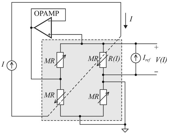
Figure 1.
Individual characterization method of one MR element of the bridge.
If the MR element is working in the linear range, its actual resistance R(I) will be given by
Ro being the MR resistance of the element at zero current and SR its resistance sensitivity. As Figure 1 shows, the operational amplifier (OPAMP) prevents any current from flowing through the bridge resistances adjacent to R(I), ensuring that all the bias current Iref flows through the element R(I) under test. In these conditions, the voltage drop across R(I) will be given by
Substituting Equation (1) into Equation (2) yields the voltage drop V(I) across the MR element:
S being the voltage sensitivity of the element. Hence, the electrical current I to be measured could be obtained by:
An instrumentation system was designed to obtain, sequentially, the linear behaviour of the four elements of the bridge, particularly the resistance Ro at zero current and their voltage sensitivity S. The main idea for the sequential characterization of the four elements is shown in Figure 2. It is based on automatically rotating the bridge terminals around the electronic circuitry needed (a current source, a high input impedance voltmeter and an OPAMP configured as a voltage follower). The rotating sequence to characterize R2, R1, R3 and R4 of Figure 2, with the current I to be measured, is depicted in Table 1.
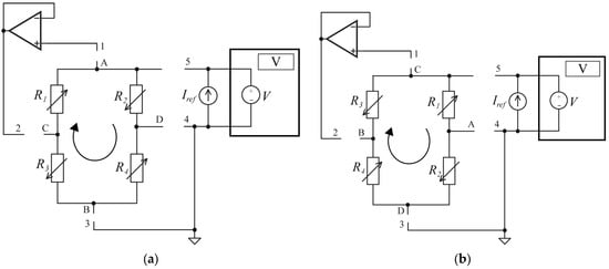
Figure 2.
Rotating procedure to sequentially characterize the resistance of the four MR elements of the bridge. (a) Characterization of R2; (b) characterization of R1.

Table 1.
Terminal connection to test the four MR elements.
Figure 3 shows the experimental set-up. The current source and the voltage meter were implemented by the source-and-measure unit (SMU) 2400 from Keithley, Cleveland, OH, USA. The OP07 biased by a ±15 V voltage source has been used as OPAMP. The current I to be sensed by the MR element was generated by a four-quadrant bipolar power supply (BOP6-125 from Kepco, Naju, Republic of Korea) circulating across a copper trace or a copper bar depending on the current level to measure. To establish the connections indicated in Table 1, a 7709-switching matrix (six rows per eight columns) from Keithley, Cleveland, OH, USA, was used, working inside the 2700 digital multimeter mainframe (from Keithley, Cleveland, OH, USA). In the present design, the OPAMP and the SMU were connected to the first two rows of the 7709-switching matrix and the bridge elements R1, R2, R3 and R4 with the first four columns, as shown in Figure 4. Notice that the system can be implemented by different available electronic hardware, i.e., replacing the switching matrix by digital controlled relays or substituting the SMU by a controllable breadboard-designed current source, as in []. However, a power current source is needed in any case to supply the electrical current measured by the element under test and its size will be determined by the maximum permissible full-scale range of the element.
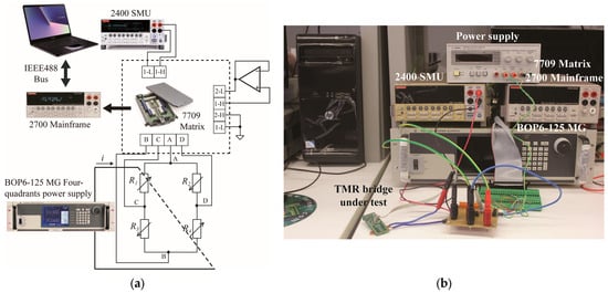
Figure 3.
(a) Block diagram of the designed instrumentation system and (b) its experimental set-up.
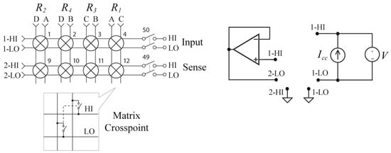
Figure 4.
Bridge and electronic equipment connections with the switching matrix.
A LabView-based routine was designed to control the electronic equipment and to carry out the acquisition process of measurements. Figure 5 shows the flow diagram and the logic states considered to implement the virtual instrument. To achieve this, the user must enter the current interval (I) that will flow through the copper conductor; the current level that will bias the element under test (Iref, provided by the SMU) and the file where all the measurements will be saved. At the end of the current sweep, the software routine will show graphically the voltage drop V(I) against electrical current I.
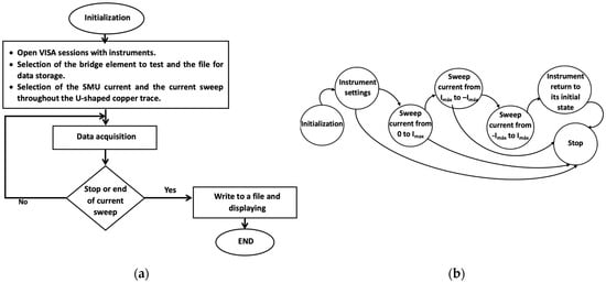
Figure 5.
(a) Flow diagram and (b) logic states of the developed virtual instrument.
With this instrumentation system, the elements of three Wheatstone MR bridges were tested, two custom-microfabricated [] and one commercially available []. The elements under test were biased with a DC current Iref provided by the SMU and subjected to an electrical DC current sweep I. The voltage V(I) generated was acquired by the 2700 mainframe.
The first custom-designed bridge, named TMR37, was implemented using TMR technology with the four elements active to the external electric field generated by the current. With a current sweep I from −10 A to +10 A and applying the rotating procedure described previously, the voltage V(I) developed by each of the four elements was acquired. Figure 6 shows measurements obtained biasing each element with Iref = 1 mA. An imbalance in sensitivities can be observed in the R2–R3 pair of the sensor bridge as well as the existence of an offset voltage at zero current, as predicted by Equation (3). Results in Figure 6 show that a deviation from the best linear fit was obtained between 0.03% and 0.3% for the ±10 A interval with a correlation coefficient between 0.994 and 0.996. In this figure, Si (i = 1, 2, 3, 4) is the voltage sensitivity of the element obtained from the best linear fit of the measurements taken.
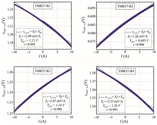
Figure 6.
Voltage drop developed by each of the four elements of the TMR37 bridge corresponding to a current sweep from −10 A to +10 A.
The instrumentation system was also used to characterize the behaviour of the four elements of a commercial bridge current sensor based on the GMR effect. In this specific case, we focused on the AAH004-00 part from NVE Corporation, Eden Prairie, MN, USA []. Figure 7 shows the experimental measurements obtained for a current sweep from −20 A to +20 A, biasing the element with Iref = 1 mA.
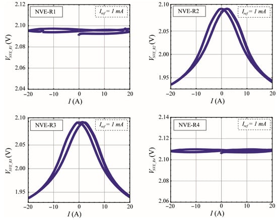
Figure 7.
Voltage drop developed by each of the four elements of a commercial GMR bridge (AAH004-00 from []) corresponding to a current sweep I from −20 A to +20 A.
Results in Figure 7 show that the MR variation with the electrical current (I) only affects two elements of the bridge (R2, R3). The other two adjacent elements (R1, R4) do not exhibit any MR variation because they are shielded from the magnetic field generated by the current, as stated in references [,,]. Additionally, it is evident from the characteristic of the active elements that the same voltage polarity corresponds to two opposite current values as it is common in this type of GMR current sensors [,,]. Notably, there is a different voltage drop path depending on the direction of the current sweep (hysteresis).
Finally, a custom-microfabricated [] full active bridge based on an SV technology MR sensor, named SV_V4, was analysed. This sensor was designed to measure higher electrical current levels. To meet this requirement, the sensor was placed a distance from a separate copper bar according to the scheme shown in Figure 8.
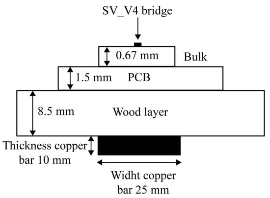
Figure 8.
Cross section view (not to scale) of the arrangement made for bridge SV_V4 to test its four MR elements for a current sweep from −125 A to +125 A. Copper bar on bottom.
Figure 9 shows experimental measurements obtained for a current sweep from −125 A to +125 A, biasing each element with Iref = 100 μA. Table 2 summarizes electrical parameters obtained from the characterization process. It shows the maximum, minimum and average values of the SV_V4 bridge elements and their % variation with respect to the average value. The magnetoresistance at zero current (offset resistance, Ro) was also calculated considering a complete current sweep cycle (0 A → +125 A → −125 A → 0 A). A maximum variation of about 0.6 Ω was observed due to the hysteresis behaviour of the magnetic materials used to implement the MR elements. In this figure, Si (i = 1, 2, 3, 4) is the voltage sensitivity of the element obtained from the best linear fit of the measurements taken.
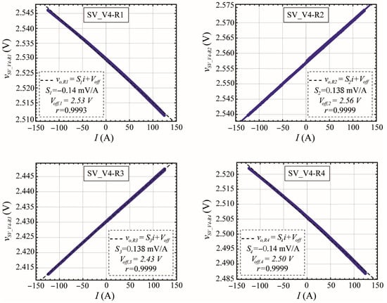
Figure 9.
Voltage drop measured between terminals of each of the four elements of the SV_V4 bridge corresponding to a current sweep from −125 A to +125 A with a polarization of Iref = 100 μA.
Table 2.
Characterization results of the elements R1, R2, R3 and R4 for the SV_V4 bridge under the 0 A → +125 A → −125 A → 0 cycle of current.
From Figure 9 and Table 2, the four elements of the bridge match MR behaviour concerning MR % variation, current sensitivity and offset resistance with good linearity within the test current interval. The measurements carried out with the designed instrumentation system also allowed us to obtain the output characteristic of the sensor bridge as well as its input resistance seen from the power terminals (Figure 10). In this figure, S is the voltage sensitivity of the bridge obtained from the best linear fit of the measurements.
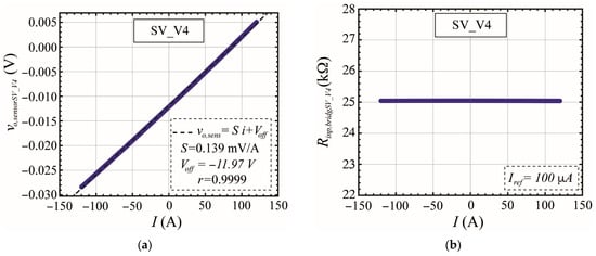
Figure 10.
(a) DC current-to-voltage characteristic of the SV4_V4 sensor bridge and (b) its input resistance seen from power supply terminals.
According to Figure 10, the response of the sensor bridge is highly linear with the current to be measured, showing a sensitivity that matches the sensitivities obtained by independently characterizing each of the four elements (see Figure 9 for their sensitivities). This result is what would be expected for a sensor bridge with the four elements active two by two. It is possible to see how the resistance of the bridge remains unchanged around 25 kΩ, corresponding to the resistance of any of the four elements at zero current (offset resistance, Ro, see also Table 2).
3. AC Current Measurement with MR Shunt and Lock-In Processing
In this section, one single element of the SV_V4 bridge (in this case R2), analysed in a previous section, has been used to monitor 50 Hz AC currents up to a maximum of 125 A peak. Figure 11 shows the electronic interface designed to process the signal from the MR element to measure the 50 Hz AC current i(t), which includes a lock-in amplifier and an electronic interface to properly convert the signal to its rms value.
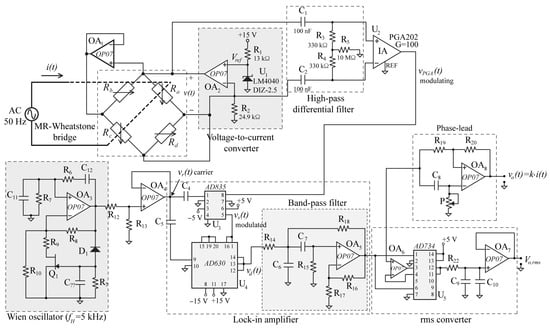
Figure 11.
Electronic interface based on lock-in processing to measure AC current by an MR shunt.
In the circuit of Figure 11, the OPAMP OA1, configured as a voltage follower, prevents the current delivered by the OPAMP OA2 from flowing through the bridge element Rb. The OA2–R1–R2–U1 components implement a current source (Vref = 2.5 V) in this design 100 μA. Thanks to OA1, Iref circulates entirely through the element of the bridge Ra.
Similar to Equation (4), the AC current i(t) to be measured can be obtained from
where the ratio v(t)/S reflects the concept of an MR shunt. The voltage v(t) generated by the sensing element Ra is associated with the current to be sensed i(t) due to the TMR effect (sensor sensitivity S). The reference current Iref flowing through Ra serves only to polarize, but the current to be sensed i(t) does not pass through it as it happens in a conventional resistive shunt, thus isolating the magnetoresistance and preventing its self-heating.
Equation (5) states that there is a DC term (Iref Ro/S) dependent on the sensor parameters S and Ro (resistance of the element at zero current). For an output v(t) dependent only on the AC current i(t) without an additional offset level, a high-pass differential filter, consisting of the network C1–C2–R3–R4 [] in Figure 11, eliminates this DC term because it does not give relevant information. Resistor R5 is necessary to provide a flow path for the input bias currents of the following instrumentation amplifier (IA) U2. In this design, the PGA202 model configured with gain G = 100 has been used []. Its output voltage vPGA(t) will act as a modulating signal for the lock-in processing
where
- peak amplitude of the sensed current (experimentally 125 A);
- (experimentally 1.75 V for the maximum value of the sensed current Ipk);
- angular frequency of the current (2 π 50 Hz);
- phase shift of the current.
The carrier signal vr(t) was implemented using a sinusoidal Wien bridge oscillator [] with automatic stabilization of the amplitude vr at this output (0.52 V). The oscillator was designed for a carrier frequency fH of 5 kHz. A suppressed carrier modulator was implemented using a four-quadrant multiplier U3, (AD835, []) whose output voltage vs(t) is given by
where
- (experimentally 0.43 V);
- (constant of the multiplier);
- .
The synchronous detection required by a lock-in amplifier is implemented by the AD630 component (U4 in Figure 11). It is configured as a synchronous demodulator with constant []. Its output voltage vd(t) will be carried out by the product:
According to Equation (8), the demodulated voltage vd(t) has frequency components in wL, 2wH + wL and 2wH − wL. A band-pass filter [] centred on wL is connected at the output of the demodulator rejecting the high-frequency components 2wH + wL and 2wH − wL. The gain kf of the filter at wL is given by (calculated as 2.65). A phase adjustment circuit (phase lead) [] is connected to compensate for time delays made by the previous circuits. Its output voltage vo(t) is proportional to the amplitude of the current to be measured and retains its frequency dependence.
with (experimentally 4.8 mV/A).
At the output of the band-pass filter, a rms-to-DC circuit was also implemented by means of the AD734 component (U5) to obtain the rms value of the voltage vo(t) [].
4. Experimental Results
In this section, the main output waveforms of the circuit in Figure 11 are presented when a 50 Hz AC current sweep i(t) up to 125 A peak is applied. The current i(t) was generated by the four-quadrant bipolar power supply (BOP6-125 Kepco, Naju, The Republic of Korea) and measured with a current probe (A603 Tektronix, Beaverton, OR, USA) as the reference. Figure 12a shows the current sensed by the reference probe and the output voltage of the designed interface corresponding to 125 A peak current i(t). A certain distortion in the sinusoidal signal is observed in the reference probe due to working close to its measurement limit, but it is not observed in the signal provided by the electronic interface. Figure 12b shows the same signals corresponding to a 10 A peak current i(t).
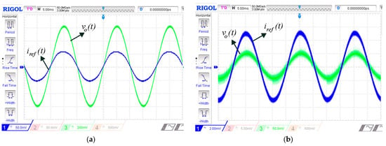
Figure 12.
(a) Green trace: output voltage provided by the electronic interface; blue trace: reference current iref(t), from an AC current probe (A6303, Tektronix) for a 125 A peak current i(t). (b) Same signals corresponding to 10 A peak current i(t).
With the values obtained for k and considering a full-scale current of 125 A, an amplitude of 0.6 V is expected for vo(t).
The MR shunt was subjected to several current sweeps recording the voltage provided by the rms-to-DC interface. Figure 13 shows the response of the rms converter to a sweep from 0 to 125 A peak.
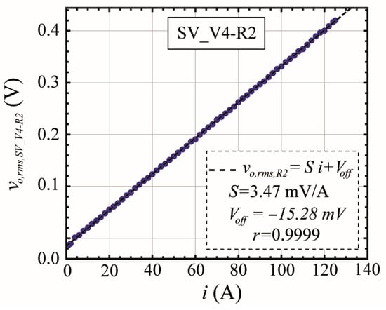
Figure 13.
Output voltage (Vo,rms) response of the rms-to-DC converter for a current variation from 0 to 125 A peak.
Figure 14 shows the response of the rms converter when current variations of 0.25 A peak amplitude are made.
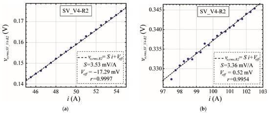
Figure 14.
Response of the rms converter in two current intervals, (a) medium interval, (b) high interval, each with a step of 0.25 A peak amplitude.
Figure 15 shows an experimental arrangement of the proposed electronic system. The sensor is located on a wooden block insulated from the copper conductive bar (arranged at the bottom, see Figure 8).
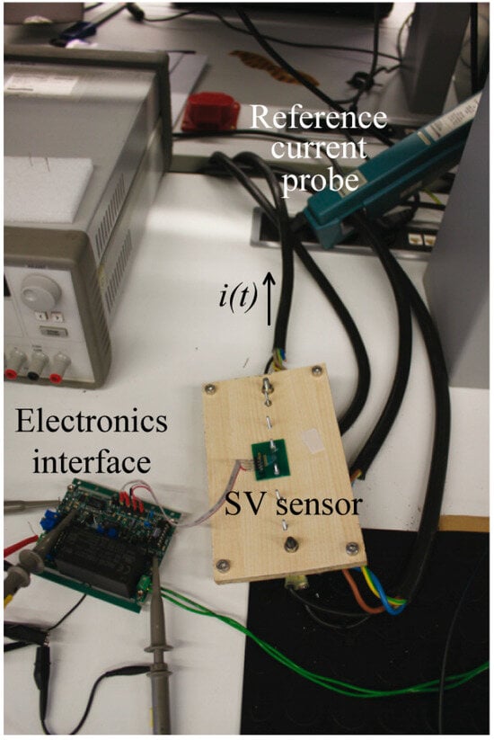
Figure 15.
Experimental set-up of the proposed electronic interface for an MR shunt.
5. Discussion
The proposed instrumentation system shown in Section 2 allows to characterize the four elements of a bridge MR sensor. The solution implemented in the work is based on test and measurement equipment available at laboratories or control quality rooms. If the four elements must be measured in industrial environments like plant production lines or in situations where various test points are needed, solutions based on electronic components and subsystems could be adopted. As an example, using a data acquisition card (DAQ) will allow us to replace the SMU by a designed current source [], measuring the voltage drop across the element by one DAQ analogue input channel. The switching actions needed by the rotating method (Figure 2 and Table 1) developed by the acquisition frame and its switching matrix could be implemented using low-cost relays controlled by the DAQ digital outputs. Nevertheless, in any case, a software installed in a computer or microcontroller unit is needed to interface and control the electronic hardware and a power unit must be used to generate the current sweep measured by the elements under test.
The results obtained in the characterization process of the bridge elements have suggested the possibility of measuring an electric current using a single bridge element as a sensor. Isolated MR elements were not available at the time the work was carried out, so an interface was developed that blocks the polarization of three bridge elements, leaving only one active, although it would be desirable to have independent elements to achieve simpler electronic interfaces.
The fully differential high-pass filter in Figure 11 must be omitted in DC current measurement applications. In this case, the offset term introduced by the sensor at zero current should be compensated (Equation (5)). However, this offset is not associated with mismatches in the manufacturing of four elements in a sensor bridge. In the case of a sensor element, the offset can be more easily controlled in the microelectronic fabrication process and its subsequent compensation is simpler by requiring a high-level positive voltage.
Synchronous demodulation prevents thermocouple effects, 1/f noise, DC drifts in the electronics or external pick-up noise from causing current measurement errors [,]. Notice that the designed electronic interface of Figure 11 allows for different developments. The carrier signal vr(t) can also be implemented by means of a square wave generator [,]. The modulator was implemented using a four-quadrant multiplier. This circuit requires a different supply voltage than the rest of the electronics (±5 V instead of ±15 V). This implies an additional conversion stage to achieve it (not included in the circuit of Figure 11). The band-pass filter limits the frequency spectrum to a band centred on the frequency of interest (line frequency), rejecting undesired frequency components such as those produced in the demodulation. While a low-pass filter would have been sufficient, a band-pass filter was chosen to further reduce potential low-frequency interferences. The final circuit implements an all-pass function [] without gain but is capable to adjust the phase of the demodulated signal by recovering the electrical current i(t) in its entire form. In this development, a phase-lead circuit was used to make the phase match with the signal offered by the reference current probe. An rms-to-DC conversion circuit was also implemented in the final stage. This conversion might not be necessary in cases where digital intelligence with sufficient computing power is available (e.g., digital signal processor or field-programmable gate arrays).
6. Conclusions
The work has proposed an instrumentation system able to characterize individually the four elements of an MR Wheatstone bridge current sensor. Based on the described rotating method, the characterization process obtains the sensitivity, offset and non-linear deviation of each element of the bridge, preserving their internal connections. Results for custom-designed and industrial sensors were obtained. The system uses cost-effective electronic equipment and some general electronic components. It can be reproduced easily in a laboratory or developed in an industrial sensor production line. It is an efficient tool to obtain statistical information of the sensor imbalances or to take decisions if the sensor parameters are or not within some specific limits of tolerance. The experimental measurements presented show that using one element (MR shunt) is enough to sense an electrical current simplifying the electronic interface. With a sensor element, the same sensitivity is obtained as with a sensor bridge but with less microelectronic complexity.
The work has proposed an electronic circuit to interface the MR shunt to a lock-in amplifier. The 50 Hz AC current measurements were both obtained in the time domain in rms format with high linearity behaviour. Peak values up to 125 A were covered with a resolution of 0.25 A. The lock-in amplifier offers great rejection capacity for low-frequency noise, high-frequency interference, offsets in the measurement chain and time drifts.
Regarding a single MR sensor element, biased with constant current, it is possible to measure the electrical current i(t) by the MR effect by only measuring the voltage drop v(t) between its terminals, as demonstrated in a conventional shunt resistor. However, the current i(t) does not physically flow through the sensor element.
Current sensing using an MR element offers application possibilities in fields such as current measurements in electrical substations, energy metering of industrial or domestic loads or to control the energy charging process in electric vehicles.
Author Contributions
Conceptualization, D.R.-M.; methodology, D.R.-M. and R.G.-G.; software, D.R.-M.; validation, D.R.-M., R.G.-G. and S.S.-D.; formal analysis, D.R.-M. and R.G.-G.; investigation, D.R.-M., R.G.-G. and S.S.-D.; resources, D.R.-M. and R.G.-G.; data curation, D.R.-M., R.G.-G. and S.S.-D.; writing—original draft preparation, D.R.-M. and R.G.-G.; writing—review and editing, D.R.-M. and R.G.-G.; visualization, D.R.-M. and R.G.-G.; supervision, D.R.-M. and S.C.; project administration, S.C.; funding acquisition, S.C. and P.P.F. All authors have read and agreed to the published version of the manuscript.
Funding
INESC MN acknowledge funding of the Research Unit from the FundaçÃo para a Ciência e a Tecnologia (FCT) through the BASE (UIDB/0536/2020) [doi: https://doi.org/10.54499/UIDB/05367/2020] and PROGRAMATICO (UIDP/0536/2020) [doi: https://doi.org/10.54499/UIDB/05367/2020] Programs. We would also like to acknowledge the funding from Project ATE: Agenda for the Energy Transition, investment project nr. 56, from the Incentive System to Mobilising Agendas for Business Innovation, funded by the Recovery and Resilience Plan and by European Funds NextGeneration EU.
Data Availability Statement
Data are contained within the article.
Conflicts of Interest
The authors declare no conflicts of interest.
References
- Jin, Z.; Arif, M.; Oogane, M.; Ando, Y. Serial MTJ-Based TMR Sensors in Bridge Configuration for Detection of Fractured Steel Bar in Magnetic Flux Leakage Testing. Sensors 2021, 21, 668. [Google Scholar] [CrossRef] [PubMed]
- Rifai, D.; Abdalla, A.N.; Razali, R.; Ali, K.; Faraj, M.A. An Eddy Current Testing Platform System for Pipe Defect Inspection Based on an Optimized Eddy Current Technique Probe Design. Sensors 2017, 17, 579. [Google Scholar] [CrossRef] [PubMed]
- Sreevidya, P.V.; Borolea, U.P.; Kadama, R.; Khana, J.; Barshiliaa, H.C.; Chowdhurya, P. A novel AMR based angle sensor with reduced harmonic errors for automotive applications. Sens. Actuators A 2021, 324, 112573. [Google Scholar] [CrossRef]
- Ripka, P.; Blažek, J.; Mirzaei, M.; Lipovský, P.; Šmelko, M.; Draganová, K. Inductive Position and Speed Sensors. Sensors 2020, 20, 65. [Google Scholar] [CrossRef] [PubMed]
- Dabek, M.; Wisniowski, P.; Kalabinskia, P.; Wronac, J.; Moskaltsova, A.; Cardoso, S.; Freitas, P.P. Tunneling magnetoresistance sensors for high fidelity current waveforms monitoring. Sens. Actuators A 2016, 251, 142–147. [Google Scholar] [CrossRef]
- Beheraa, B.; Borolea, U.P.; Sivajia, A.; Khana, J.; Kumarb, P.; Ananda, C.M.; Barshiliaa, H.C.; Chowdhurya, P.; Jadhavd, J.J. Design and development of GMR based low range pressure sensor for medical ventilator application. Sens. Actuators A 2021, 321, 112581. [Google Scholar] [CrossRef]
- Ouyanga, Y.; Wanga, Z.; Zhaoa, G.; Hua, J.; Jia, S.; Hea, J.; Wang, S.X. Current sensors based on GMR effect for smart grid applications. Sens. Actuators A 2019, 294, 8–16. [Google Scholar] [CrossRef]
- Parkin, S.S.P.; Kaiser, C.; Panchula, A.; Rice, P.M.; Hughes, B.; Samant, M.; Yang, S.H. Giant tunneling magnetoresistance at room temperature with MgO (100) tunnel barriers. Nat. Mater. 2004, 3, 862–867. [Google Scholar] [CrossRef] [PubMed]
- Freitas, P.P.; Ferreira, R.; Cardoso, S.; Cardoso, F. Magnetoresistive sensors. J. Phys. Condens. Matter 2007, 19, 165221. [Google Scholar] [CrossRef]
- Freitas, P.P.; Ferreira, R.; Cardoso, S. Spintronic Sensors. Proc. IEEE 2016, 104, 1894–1918. [Google Scholar] [CrossRef]
- Ravelo, S.I.; Ramírez, D.; Cardoso, S.; Ferreira, R.; Freitas, P.P. Total ionizing dose (TID) evaluation of magnetic tunnel junction (MTJ) current sensors. Sens. Actuators A 2015, 225, 119–127. [Google Scholar] [CrossRef]
- Sensitec, Magneto Resistive Current Sensors. Available online: https://www.sensitec.com (accessed on 15 July 2024).
- Non-Volatile Electronics. Available online: https://www.nve.com/#&panel1-2 (accessed on 15 July 2024).
- Honeywell. Available online: https://sensing.honeywell.com/sensors/linear-and-angle-sensor-ics (accessed on 15 July 2024).
- Sánchez, J.; Ramírez, D.; Amaral, J.; Cardoso, S.; Freitas, P.P. Electrical ammeter based on spin-valve sensor. Rev. Sci. Instrum. 2012, 83, 105113. [Google Scholar] [CrossRef] [PubMed]
- Lopes, A.; Cardoso, S.; Ferreira, R.; Paz, E.; Deepak, F.L.; Sánchez, J.; Ramírez, D.; Ravelo, S.I.; Freitas, P.P. MgO Magnetic Tunnel Junction Electrical Current Sensor with Integrated Ru Thermal Sensor. IEEE Trans. Magn. 2013, 49, 3866–3869. [Google Scholar] [CrossRef]
- Ramírez-Muñoz, D.; García-Gil, R.; Cardoso, S.; Freitas, P. Characterization of Magnetoresistive Shunts and Its Sensitivity Temperature Compensation. Sensors 2024, 24, 3047. [Google Scholar] [CrossRef] [PubMed]
- Baker, N.; Dupont, L.; Beczkowski, S.M.; Iannuzzo, F. Proof-of-Concept for an On-Chip Kelvin-Emitter RTD Sensor for Junction Temperature Monitoring of IGBTs. IEEE Trans. Compon. Packag. Manuf. Technol. 2024; early access. [Google Scholar] [CrossRef]
- Elangovan, K.; Chandrika, A. An Efficient Digital Readout for Four-Lead Resistance Thermometers. IEEE Sens. Lett. 2023, 7, 6009504. [Google Scholar]
- Kumar, S.; De, R.; Kumar, A.; Kumar, S. Novel MEMS Piezoresistive Sensor with Hair-Pin Structure to Enhance Tensile and Compressive Sensitivity and Correct Non-Linearity. J. Electron. Test. 2020, 36, 509–517. [Google Scholar]
- Haisheng San, H.; Zhang, H.; Zhang, Q.; Yu, Y.; Chen, X. Silicon-glass-based single piezoresistive pressure sensors for harsh environment applications. J. Micromech. Microeng. 2013, 23, 075020. [Google Scholar]
- Meena, K.V.; Mathew, R.; Leelavathi, J.; Ravi Sankar, A. Performance Comparison of a Single Element Piezoresistor with a Half-Active Wheatstone Bridge for Miniaturized Pressure Sensors. Measurement 2017, 111, 340–350. [Google Scholar] [CrossRef]
- Wilmshurst, T.H. Phase-sensitive Detectors Methods. In Signal Recovery from Noise in Electronic Instrumentation, 2nd ed.; CRC Press: Boca Raton, FL, USA, 1990; pp. 29–43. ISBN 9780750300582. [Google Scholar]
- Gerstenhaber, M.; Murphy, M. Synchronous System Measures µΩs, Analog Devices. Available online: https://www.analog.com/media/en/technical-documentation/application-notes/AN-306.pdf (accessed on 15 July 2024).
- Blair, D.P.; Sydenham, P.H. Phase sensitive detection as a means to recover signals buried in noise, 1975. J. Phys. E Sci. Instrum. 1975, 8, 621. [Google Scholar] [CrossRef]
- Sydenham, P.H.; Thorn, R. (Eds.) Handbook of Measurement Science, Signal-to-Noise Ratio Improvement. In Volume 1: Theoretical Fundamentals; John Wiley & Sons: New York, NY, USA, 1996; pp. 444–459. ISBN 978-0-471-10037-9. [Google Scholar]
- Analog Devices. Available online: https://www.analog.com/en/products/ad630.html (accessed on 15 July 2024).
- Meade, M.L. Basics concept in lock-in recovery. In Lock-in Amplifiers: Principles and Applications; Peregrinus, P., Ed.; IEE Electrical Measurement Series; Institution of Engineering and Technology: London, UK, 1983; pp. 7–30. [Google Scholar]
- Pallás-Areny, R.; Webster, J.G. Amplitud Demodulation. In Analog Signal Processing; John Wiley & Sons: New York, NY, USA, 1999; pp. 255–269. ISBN 0471125288. [Google Scholar]
- Smith, C.H.; Schneider, R.W. Low Field Magnetic Sensing with GMR Sensors. In Proceedings of the Sensors EXPO, Baltimore, MD, USA, 5–7 May 1999. 13p. [Google Scholar]
- Smith, C.H.; Schneider, R.W. The Growing Role of Solid-State Magnetic Sensing. In Proceedings of the Sensors EXPO, Detroit, MI, USA, 21–22 March 1997; pp. 139–149. [Google Scholar]
- Daughton, J.; Brown, J.; Chen, E.; Beech, R.; Pohm, A.; Kude, W. Magnetic Field Sensors Using GMR Multilayer. IEEE Trans. Magn. 1994, 30, 4608–4610. [Google Scholar] [CrossRef]
- Casas, O.; Pallás-Areny, R. Basics of Analog Differential Filters. IEEE Trans. Instrum. Meas. 1996, 45, 275–279. [Google Scholar] [CrossRef]
- Texas Instruments. Available online: https://www.ti.com/lit/ds/symlink/pga202.pdf (accessed on 15 July 2024).
- Franco, S. Signal Generators. In Design with Operational Amplifiers and Analog Integrated Circuits, 4th ed.; McGraw-Hill Education, Inc.: New York, NY, USA, 2015; pp. 541–548. ISBN 978-0-07-802816-8. [Google Scholar]
- Analog Devices. Available online: https://www.analog.com/en/products/ad835.html (accessed on 15 July 2024).
- Mancini, R. Active Filter Design Techniques. In Op Amps for Everyone; Texas Instruments: Dallas, TX, USA, 2002; pp. 16-27–16-33. Available online: http://web.mit.edu/6.101/www/reference/op_amps_everyone.pdf (accessed on 15 July 2024).
- Stout, D.F.; Kaufman, M. Time and Phase Circuits. In Handbook of Operational Amplifier Circuit Design; McGraw-Hill: New York, NY, USA, 1976; pp. 26-1–26-5. [Google Scholar]
- Analog Devices. Available online: https://www.analog.com/en/products/ad734.html (accessed on 15 July 2024).
- Stitt, R.M. Implementation and Applications of Current Sources and Current Receivers, Texas Instruments. Available online: https://www.ti.com/lit/an/sboa046/sboa046.pdf (accessed on 15 July 2024).
Disclaimer/Publisher’s Note: The statements, opinions and data contained in all publications are solely those of the individual author(s) and contributor(s) and not of MDPI and/or the editor(s). MDPI and/or the editor(s) disclaim responsibility for any injury to people or property resulting from any ideas, methods, instructions or products referred to in the content. |
© 2024 by the authors. Licensee MDPI, Basel, Switzerland. This article is an open access article distributed under the terms and conditions of the Creative Commons Attribution (CC BY) license (https://creativecommons.org/licenses/by/4.0/).