Article

Multifrequency Impedance Characterization for Radio Frequency Identification Chip

1
RFID-OC Team of the ACSE Department, IM2NP UMR 7334, ISEN Yncrea Mediterranée Place G. Pompidou, 83000 Toulon, France
2
STMicroelectronics, Avenue COQ, 13790 Rousset, France
*
Author to whom correspondence should be addressed.
Electronics 2024, 13(15), 3059; https://doi.org/10.3390/electronics13153059
Submission received: 31 May 2024 / Revised: 14 July 2024 / Accepted: 16 July 2024 / Published: 2 August 2024

Abstract

:
This article introduces an innovative methodology for measuring the impedance of RFID (Radio Frequency Identification) chips. The primary objective is to develop a technique that enables impedance measurement across a range of frequencies, centered around the critical operational frequency of RFID systems, specifically 13.56 MHz. Unlike conventional methods, which typically focus solely on the impedance at 13.56 MHz, this approach utilizes the reflection coefficient of the device under test (DUT) to measure impedance over a broader frequency spectrum. This spectrum encompasses the frequencies within the ISO14443 communication bandwidth. The excitation signal is carefully selected to closely mimic an actual RFID communication frame. The experimental results demonstrate the feasibility of this method by comparing the impedance measurements of passive component pairs against those obtained using a vector network analyzer (VNA). Subsequently, the technique is applied to an RFID chip, underscoring its practical applicability and accuracy.

1. Introduction

Radio Frequency Identification (RFID) is a wireless communication technology that operates on RF communication through magnetic coupling using AM modulation at 13.56 MHz. RFID systems are composed of two primary elements: the reader, also known as the proximity coupling device (PCD); the tag, referred to as the proximity integrated circuit card (PICC). The PICC, which contains an integrated circuit (IC), is powered by the magnetic field generated by the PCD. Communication between the PCD and PICC is facilitated by backscattering, also known as load modulation, where the PICC modulates the signal transmitted by the PCD.
Passive high-frequency (HF) RFID chips are extensively utilized for object identification and tracking across various sectors such as logistics, inventory management, access control, and product traceability. The performance and reliability of RFID systems are critically dependent on the characteristics of the RFID chips. Consequently, characterizing these chips is essential to ensure their optimal functionality in specific application environments like in payment transaction or in identification [1,2]. This characterization involves determining the chips’ electrical and electromagnetic properties, including supply voltage, current consumption, and impedance.
Understanding these properties is crucial for selecting the most suitable RFID chips for particular applications and ensuring their interoperability with different readers available on the market. Manufacturers aim to develop generic products that meet the needs of a broad range of integrators for diverse end-user needs, such as electronic payments, identity verification, and access control. The constraints faced by integrators can vary significantly based on operating conditions, including temperature, magnetic field intensity, bit rate, and operating distance. In-depth knowledge of a chip’s characteristics allows for the optimization of its integration environment, thereby maximizing its potential. Additionally, this knowledge can help direct parts produced during manufacturing to the most appropriate applications and recover parts considered defective by placing them in favorable environments, thereby reducing production losses and carbon footprint.
Several methods for measuring chip characteristics exist [3,4,5,6]. Many of these rely on network parameter measurements [3,5], particularly the reflection coefficient, S11, at the carrier frequency of 13.56 MHz. All these methods are used in direct contact with wires. With no use of coil antennas, the purpose is to measure the RFID chip’s impedance on a power range independently of magnetic coupling. However, this study proposes a novel approach that extends the analysis to a broader frequency spectrum. This paper presents a methodology for the impedance characterization of passive HF RFID chips, emphasizing not only the carrier frequency but also all frequency components constituting the signal.
An AM type B signal is selected to power the device under test (DUT), as its spectrum includes frequencies found in real communication scenarios, with a well-distributed power proportion among different frequencies. A real communication is a signal that can be found during a transaction payment or during an identification process. To validate this methodology, it is initially applied to elementary passive systems, and the results are compared with reference values obtained using a vector network analyzer (VNA). Subsequently, the method is applied to RFID chips, modeling their impedance through a parallel resistor–capacitor circuit, a widely used model in the literature [7].
Based on the impedance characteristics of a chip as a function of frequency, adjustments in both amplitude and phase of each frequency component of the signal are performed. This pre-distorted signal is designed to emulate the signal that would be obtained if combined with an antenna in a field use case, ensuring that the chip receives the expected power proportion for each frequency. The cumulative power of all frequencies corresponds to a signal with temporal characteristics emulating an RFID communication signal. The ultimate goal is to emulate RFID communication in direct contact, observe the chip’s characteristics, and certify its correct operation.

2. Quality Criteria Definition

2.1. Introduction

The objective of this method is to find the behavior of an RFID card chip by emulating the communication between a reader and a card within RFID systems. This necessitates characterizing the chip across the entire spectrum of frequencies that constitute the modulated signal, ensuring the appropriate power ratio among the different frequency components.
To accurately determine the chip’s characteristics as a function of frequency, it is essential to take into account both the accepted and reflected signals by the chip. Given that signal strength diminishes with increasing frequency, acquiring the highest frequency components presents a significant challenge. An initial step involves evaluating the frequency ranges that need characterization based on the target communication bit rate. The selected frequency range should enable the emulated signal to conform to normative quality criteria.
The first critical step is to identify the minimum frequency range required to accurately reconstruct an RFID signal. Through signal correction, it is possible to pre-distort the emitted signal to resemble the actual operating signal, while considering the established quality criteria. This approach ensures that the emulated signal accurately reflects real-world RFID communication scenarios, facilitating a comprehensive understanding of the chip’s behavior.

2.2. Processing Method

The process for determining the minimum frequency range necessary to reconstruct a typical signal in RFID communications is outlined below and illustrated in Figure 1:
-
Generate an “ideal” target signal in MATLAB with consistent rise and fall times throughout the entire frame length, and noise free.
-
Perform a fast Fourier transform (FFT) on this target signal to obtain its frequency spectrum. It is the upper grey arrow on Figure 1.
-
Select a portion of the frequency range around the carrier frequency from the target signal’s spectrum.
-
Reconstruct a transient signal using this restricted spectrum via an inverse fast Fourier transform (IFFT), producing our reconstructed signal. This is represented by the bottom grey arrow on Figure 1.
-
Perform I/Q demodulation on both the transient signals to obtain signal envelopes.
-
Compare the transition times and envelope amplitudes of the target and reconstructed signals.
-
To determine the minimum frequency range, iterate the process by progressively widening the frequency range around the selected carrier frequency. The carrier frequency, denoted as “fc”, is 13.56 MHz.
Two quality criteria are used to study the frequency range required for the next step: the first is the state transition times, between the rising edge and the falling edge of the waveform. Tolerance values are given in the RFID system standard [1]. Table 1 shows the tolerances according to bit rate.
The second criterion is the signal envelope. A point-to-point difference is made between the original signal and the reconstructed one. This verifies that the amplitude difference does not exceed a certain percentage. The study was carried out for different percentages, but the one chosen was 0.5%. This value was chosen because it is the most difficult required by the standard. Table 2 shows the envelope tolerance found in the ISO 14443 RFID product standard [1], depending on the communication rate. As described in the norm [1], type A is an AM signal with an index modulation of 100%, where three sequences, called X, Y, and Z, are used to code the information on a carrier at 13.56 MHz. The X sequence codes a 1 logic and the Y sequence codes a 0 logic. The Z sequence is used if the communication starts with a 0 or if we have two or more contiguous instances of 0. This prevents the loss of synchronization between the PCD and the PICC. Type B is an AM signal with an index modulation varying between 10 and 30%; a logic 0 is a code with a modulated sequence and a logic 1 is a code with an unmodulated sequence.
The entire communication frame is meticulously analyzed. If any single transition time or point fails to meet the tolerance defined by the quality criterion, the frequency range is deemed to be insufficient for accurate signal reconstruction, necessitating an expansion of the frequency range.
The signals utilized in this study are typical of those employed in RFID systems, a type B AM signal will be used, with a modulation index of 10%. The logical information coded by signal is not a suite of logical 01010101, …; rather, it is a random scheme. Each frame during 1 ms to ensure consistent discretization in the frequency domain across frames.
The study examines a set of signals with varying bit rates, presenting results for three specific bit rates: fc/128, fc/16, and fc/2. These bit rates are selected to cover the entire range encountered in contemporary RFID communications, from the slowest (fc/128) to the fastest (fc/2), including an intermediate rate (fc/16).
For each bit rate, state transition times, which vary according to RFID communication standards, are also considered. The goal is to encompass the widest possible range, with transition times derived from the standard depending on the bit rate. The study includes a set of rise and fall times that adhere to the specified tolerances, represented as points within a diamond diagram (Figure 2). Each capital letters represent the fall and rise time values between the rising edge and the falling edge of the waveform, for several bit rate.
Point D: Represents the least restrictive transition times, corresponding to the slowest rise and fall times.
Point A: Represents the fastest transition times. Although the standard specifies zero transition times for point A, a practical bound of 1/fc is used in this study.
Point G: Represents an intermediate transition time.
This study does not consider scenarios with differing rise and fall times, as the frequency spacing for such cases is narrower than for the fastest rise times.
In the standards, the values of the rise and fall times are different for the points in the diamond for each bit rate. The rise time for the D point for a bit rate of fc/128 is equal to 16; this means that, to go from a 0 logic to a 1 logic, the signal ramps up during 16 periods of the carrier frequency (a carrier frequency at 13.56 MHz has a period of 73.74 µs). At point D, for a bit rate of fc/16, the rise time has to be 8. Points G and D use the values of the norm.

2.3. Results

Following the application of the previously described method to signals corresponding to points D, G, and A, and at bit rates fc/128, fc/16, and fc/2, the results are summarized in Table 3. This table displays the outcomes based on bit rate and the associated transition time point, in accordance with the tolerance criteria set by the standard for transition times and an envelope percentage of 0.5%.
The results show with the Table 3 indicate the compliance of each signal with the specified tolerance criteria for transition times and the envelope, providing a clear assessment of the frequency range required for accurate signal reconstruction across different bit rates and transition times.

2.4. Discussion

With the results from the previous section presented in Table 3, the lower limit of the frequency range that is necessary to reconstruct signals correctly, in accordance with the quality criteria set out in Section 2.2, is determined to be 1 MHz. This limit ensures the accurate reconstruction of signals for various data rates and transition times.
The upper limit of the frequency range appears to be dependent on the speed of the transition times: the faster the transition from one state to another, the wider the required frequency range is. Similarly, a higher data rate necessitates a broader frequency range. For the most restrictive transition times (point A), the upper limit of the frequency range is 38.4 MHz for a data rate of fc/128 and 48 MHz for a data rate of fc/16. For the fc/2 rate, a wider bandwidth is required for the point with the slowest transition times (point D). At this point, the transition time exceeds the time required to maintain a state, leading to an erosion of the modulation index. This phenomenon seems to need a broader frequency range for accurate signal reconstruction. The upper limit for the fc/2 rate is 53.64 MHz.
This preliminary study allows us to determine the set of frequency ranges that are necessary to reconstruct signals as closely as possible to the expectations of the RFID standards. Our impedance measurement method must, therefore, provide results within these frequency ranges to be valuable in future work. By characterizing a device over a frequency range from 1 to 55 MHz, it will be possible to consider the chip characteristics so that the power accepted by the chip emulates the desired signal.

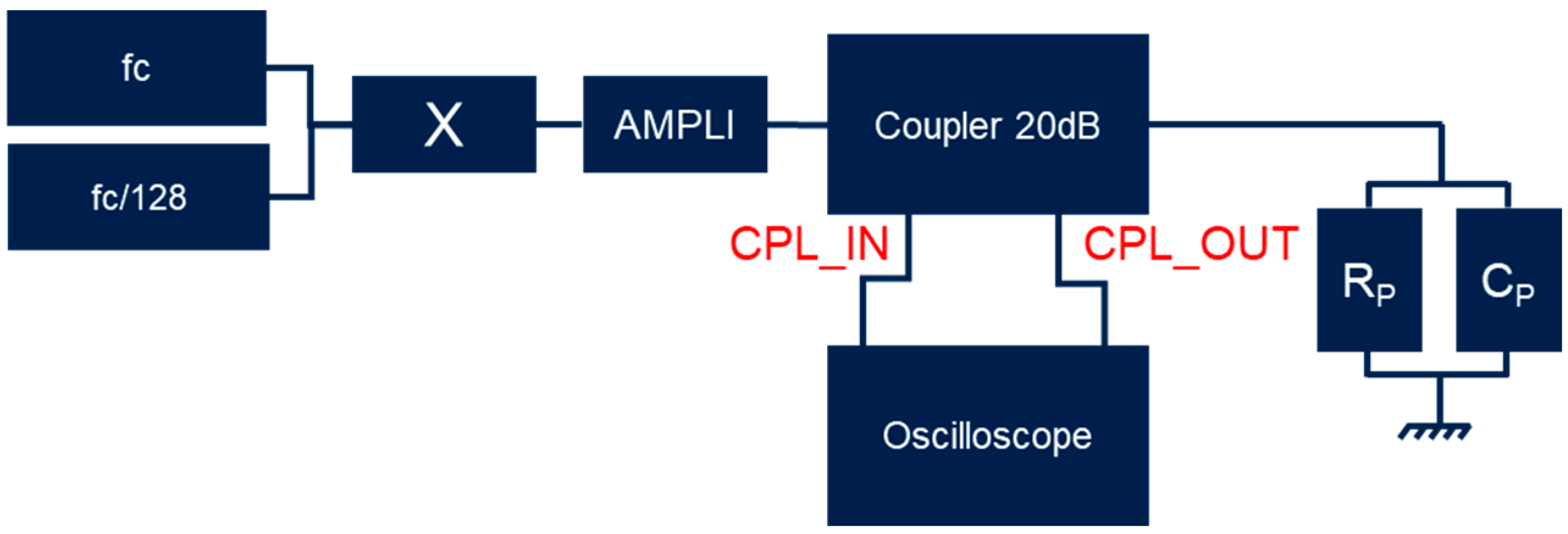
3. Multifrequency Impedance Measurement

3.1. Measurement Principle

The calculation of the impedance value is based on the knowledge of the ratio between the wave reflected by the DUT and the wave delivered to it. To obtain an image of each of these two waves, a bidirectional coupler is used. A coupler with 20 dB attenuation between the main and coupled ports was selected, as this attenuation level enables minimal power absorption to occur while maintaining a sufficient signal-to-noise ratio (SNR) to visualize the waves on the coupled channels with minimal noise impact.
s 11 ( f ) = R V D w a v e ( f ) F W D w a v e ( f ) ,
Using the obtained reflection coefficient value, it is possible to determine the impedance value associated with the DUT. The relation between the reflection coefficient and the impedance value of the DUT is given by Equation (2). Z0 is the characteristic impedance used to normalize all impedances, with the one used by the generator, at 50 Ohms.
Z D U T ( f ) = Z 0 1 + S 11 ( f ) 1 S 11 ( f ) ,
Using the obtained impedance value of the DUT, it is possible to determine the values of the components associated with a given model. The representation of the RFID chip impedance is a parallel capacitor/resistor pair. Cp represents the parallel capacitor. Rp represents the parallel resistor. YDUT is the admittance, the inverse of the impedance. The admittance is used to simplify the equation to represent the system via a pair of parallel components. The values of the components in this pair can be obtained from the following Equations (3)–(5):
Y D U T ( f ) = 1 Z D U T ( f ) ,
R p ( f ) = 1 r e a l ( Y D U T ( f ) ) ,
C p ( f ) = i m a g ( Y D U T ( f ) ) 2 π f ,
In previous work, this method was applied to monochromatic (or unmodulated) signals [6,7]. However, in this study, the aim is to extend the measurement over a frequency range. The use of spectra enables the determination of the reflection coefficient for each of the signal frequencies of interest. This procedure is also applied to the signals used for bench calibration.
The calibration type used for the measurements is SOL, which includes short, open, and load calibrations. This step enables the obtention of error terms that are subsequently applied to the device under test (DUT) measurement results. Calibration is needed for each bit rate, and the various error terms are calculated for each of the signal frequencies of interest using Equations (6)–(8) (EDF—forward directivity; ESF—forward source match; ERF—forward reflection tracking) [8].
EDF ( f ) = S 11 L O A D ( f ) ,
ESF ( f ) = S 11 _ O P E N ( f ) + S 11 S H O R T ( f ) 2 E D F ( f ) S 11 _ O P E N ( f ) S 11 _ S H O R T ( f ) ,
ERF ( f ) = 2 ( S 11 _ O P E N ( f ) E D F ( f ) ) ( S 11 S H O R T ( f ) E D F ( f ) ) S 11 _ O P E N ( f ) S 11 _ S H O R T ( f ) ,
Once these error terms have been calculated, a correction is made to the reflection coefficient value obtained from the DUT measurement using Equation (9).
S 11 M ( f ) = S 11 ( f ) E D F ( f ) E S F ( f )   S 11 ( f ) E D F ( f ) + E R F ( f )

3.2. Measurement Setup

The measurement setup is shown in Figure 3. The DUTs are mounted on a printed circuit board (PCB) that can accommodate an RFID chip. A 2.54 mm connector is used to insert a differential or passive probe, which enables the measurement of the voltage available at the DUT terminals. A set of pins is connected to the various ports in the chip package, allowing access to the internal product voltages. An SMA connector connects the PCB to the measurement environment.
An arbitrary signal generator (AWG) is used to generate modulated or unmodulated frames. An important consideration is the choice of excitation signal. The aim of this step is to determine the frequency characteristics of the chip. Different types of signals can be used to excite the DUT over a given frequency range. However, the excitation signal must necessarily be at a frequency of 13.56 MHz (called fc). This frequency is used to polarize our chip and provide the power needed to bring the chip into an operating state. Additionally, other frequencies are needed to study the chip’s response.
One approach would be to add a frequency sweep to our fc frequency signal. However, it is unclear whether the chip reacts in the same way to a wave composed of only two frequencies—fc and the frequency used in the sweep—as it does to a wave composed of several frequencies, like a typical RFID signal. To avoid this problem, we used a signal as close as possible to a conventional communication signal. We chose a type B amplitude-modulated signal. The DUT is excited with this type of signal, with a constant modulation scheme, alternating between modulated and unmodulated parts. This type of signal has the advantage of exciting the DUT with frequencies present in the signals used in RFID communications. It also has the advantage of spectrally consistent power dispersion with RFID communication signals.
The measurement environment also includes a bidirectional coupler, which collects a portion of the incident wave offered to the chip and the wave reflected by the chip. These signals are used to calculate the impedance of the DUT over a given frequency range. An oscilloscope acquires all the frames used in post-processing. An RF amplifier can be added to exceed the 23 dBm provided by the AWG. All this equipment is managed remotely using a Python program, which controls the bit rate, power range, and data files.

4. Validation of the Method on Passive Components
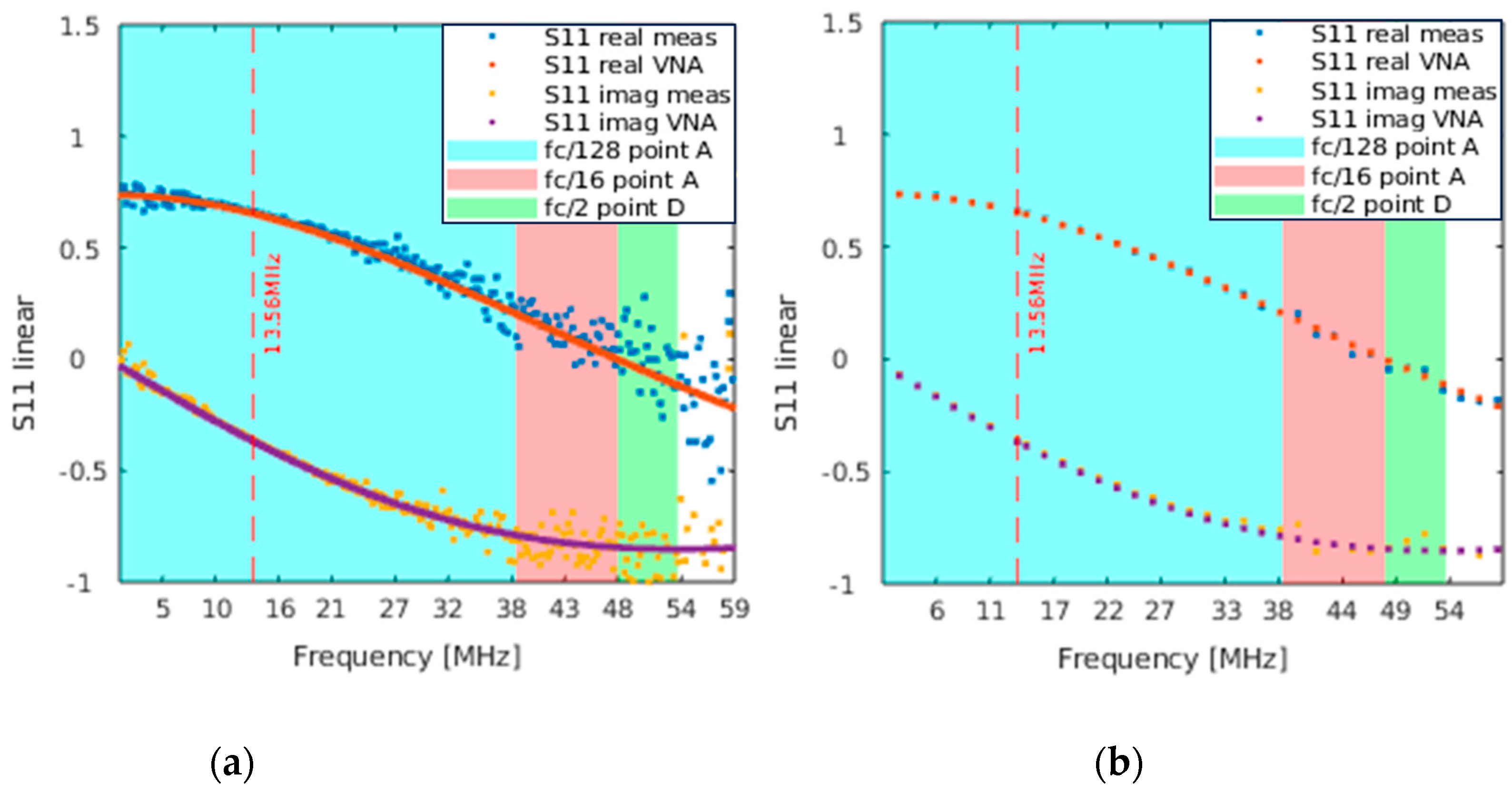
4.1. S11 Measure

The objective of this section is to demonstrate that the proposed method can be used to obtain accurate reflection coefficient and impedance values over a wide frequency range. The frequency range of interest is from 1 MHz to 55 MHz. To validate the method, it is first applied to a pair of passive components, specifically an RpCp pair, which is the model commonly used to represent an RFID chip [7]. The measurement environment described in Section 2.2 is used for this purpose. For the discrete component pair, a parallel resistance of 330 Ohms and a parallel capacitance of 56 pF are chosen. Measurements are taken with several bit rates, specifically fc/128, fc/64, fc/32, and fc/16. However, only the results for fc/128 and fc/16 are relevant and presented here.
To obtain a reference value, a measurement of the component pair is performed using a vector network analyzer (VNA).
The results obtained using the proposed multifrequency method are presented in Figure 4a. The measurements were taken with a bit rate of fc/128 and a generator setpoint power of 10 dBm. The red and purple curves in the figure represent the real and imaginary parts of the reflection coefficient, respectively, measured using a vector network analyzer (VNA) with a passive component pair. The blue and yellow points in the figure represent the real and imaginary parts of the reflection coefficient, respectively, measured using the proposed method.
As shown in the figure, the results obtained using the proposed method are consistent with the reference values obtained using the VNA. However, the measurements begin to diverge beyond a certain frequency range. This divergence appears to be due to the deterioration of the SNR as the power decreases with increasing distance from the carrier frequency of the signal.
To improve the accuracy of the reflection coefficient measurement over a wider frequency range, two approaches can be considered. The first approach is to increase the power of the input signal. The second approach is to increase the bit rate of the communication signal. By increasing the bit rate, the frequencies of the modulating signal are further away from the carrier frequency and stronger, which should improve the SNR over a wider frequency range. However, this comes at the expense of spectral richness, as there are fewer frequencies in the frequency range.
Figure 4b shows a comparison of the reflection coefficient of the passive component pair measured using the proposed method with an exciter signal having a bit rate of fc/16. As expected, increasing the bit rate improves the accuracy of the reflection coefficient measurement over the entire frequency range. However, the number of frequency measurement points is reduced, which could be a problem for systems with reflection coefficients that vary significantly over small frequency ranges. In such cases, interpolation may be difficult, and a polynomial fit may be necessary to obtain intermediate values.

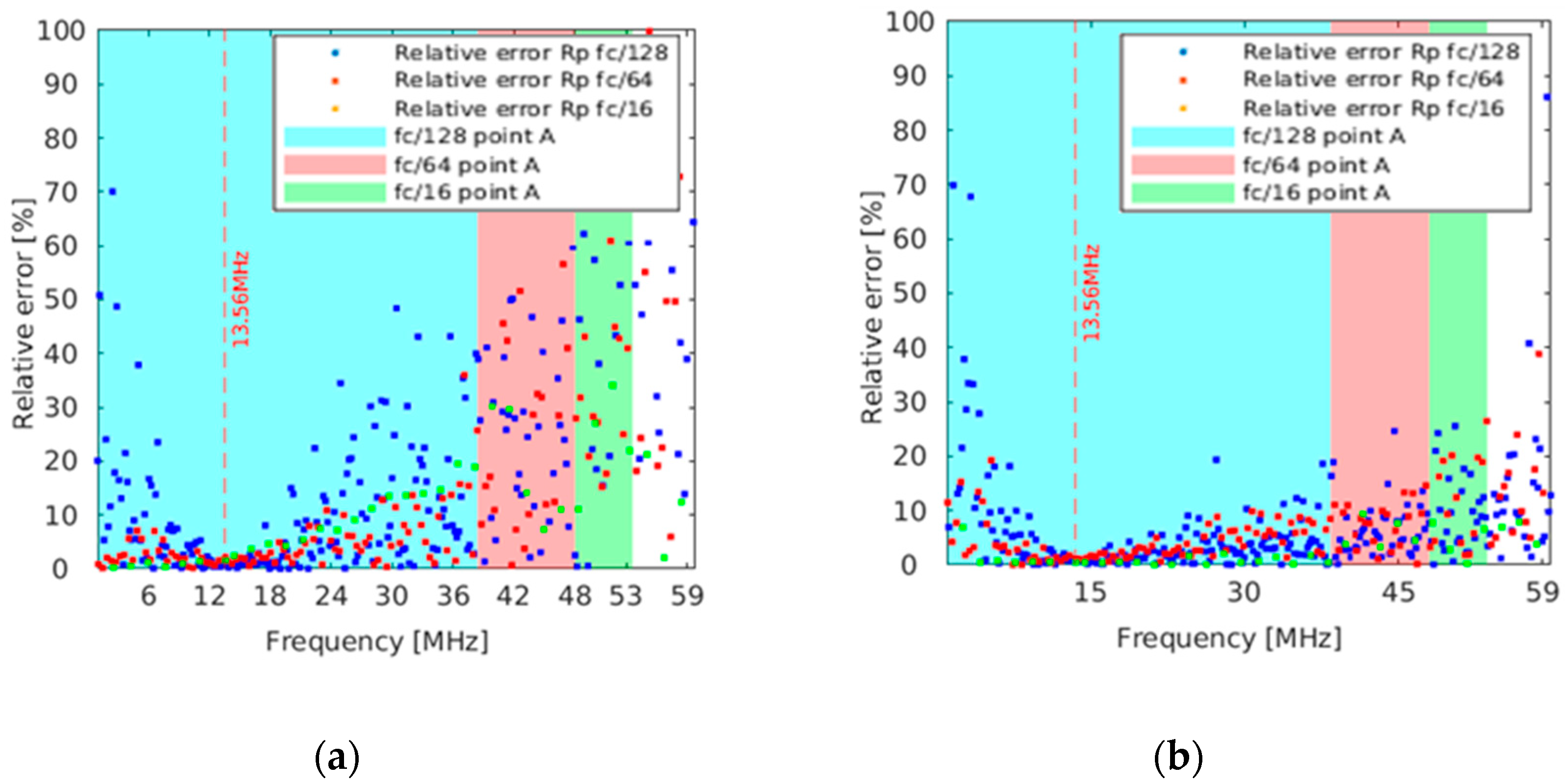
4.2. Equivalent RpCp Model

Using the reflection coefficient measurements obtained from the multifrequency method and Equations (1)–(5), it is possible to determine the equivalent component values of a parallel resistor–capacitor pair for all signal frequencies of interest. The results are presented in Figure 5, which shows the impedance of the parallel resistor and capacitor measured for two different bit rates. The left side of the figure corresponds to a bit rate of fc/128, while the right side corresponds to a bit rate of fc/16.
Based on the information provided, it appears that using a frame rate of fc/16 is sufficient to achieve accurate measurements of the components of an RpCp pair over the entire frequency range of 1 MHz to 55 MHz, with an accuracy of under 30%. This is shown in Figure 6.
The goal of the measurement is to characterize a chip within its operating range where communication is possible. For the chip being studied, the power-on reset (POR) is approximately 10 dBm. The POR is determined by sending an REQA command to the chip and gradually increasing the power delivered to the chip until it begins to respond. The power at which the chip responds is considered to be the POR. It is important to note that system protections start to activate around 15 dBm.
The information provided suggests that the multifrequency method proposed in this study can be used to accurately measure the reflection coefficient and impedance of a chip within its operating range, using a frame rate of fc/16. This method can be useful for characterizing RFID chips and other passive components in various applications.

5. On Chip Measurement

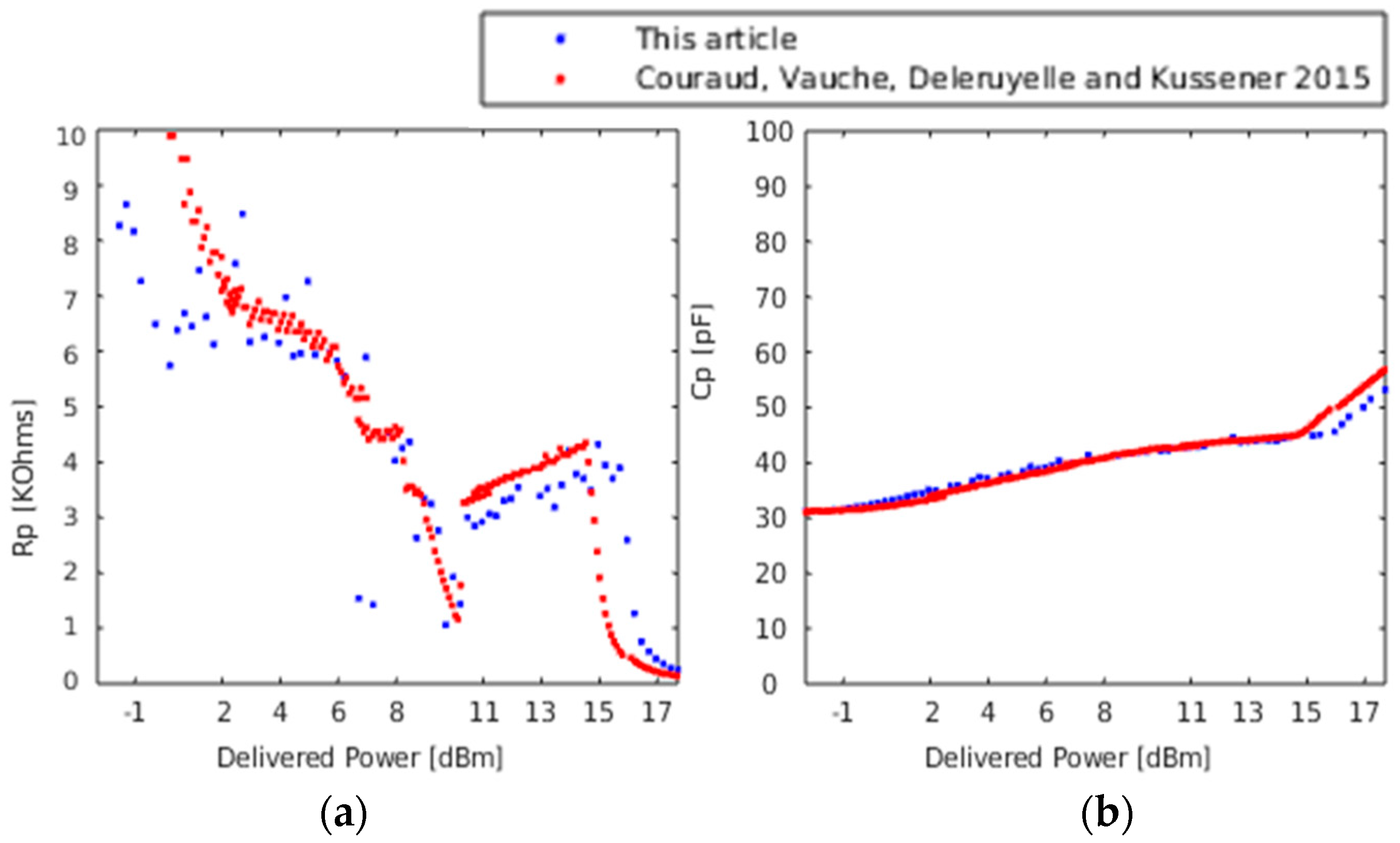
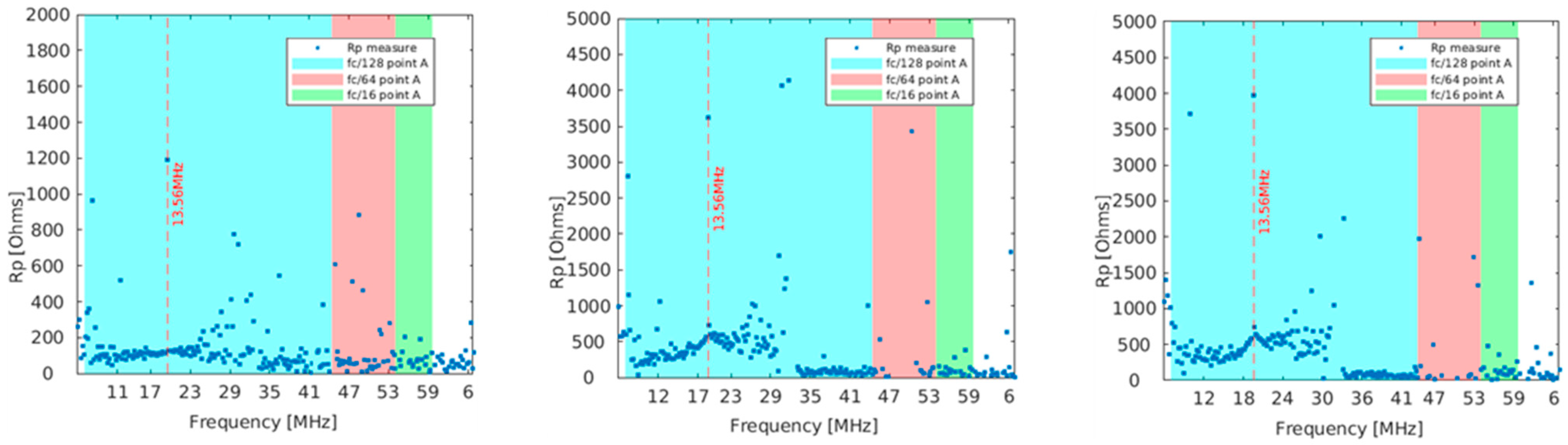
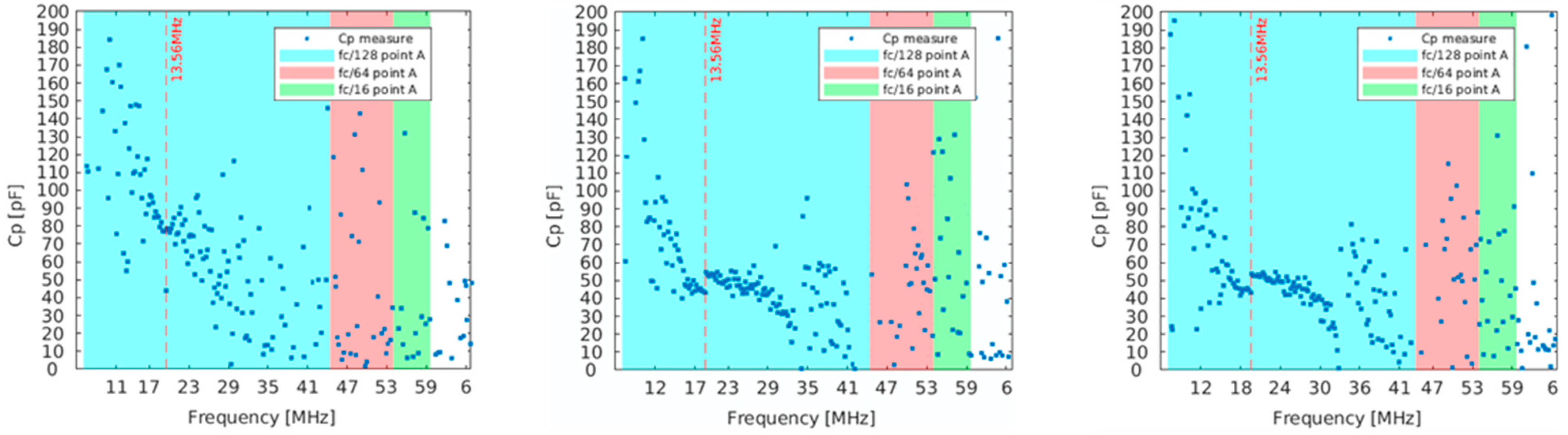
5.1. Mono-Frequency Comparison

Applying the multifrequency method to an RFID chip, the first step is to consider only the carrier frequency of the signal. The obtained results are compared with the impedance results obtained using another method, as described in Ref. [5]. In both methods, the chip impedance is measured upon contact with the wire. Figure 7 shows the comparison of the parallel resistance and capacitance values that were obtained using the two methods for an RFID chip.
The results obtained using the multifrequency method are consistent with those obtained using the reference method. However, there is an offset of approximately 1 dBm at the point where the chip’s protection systems activate, causing a significant drop in the parallel resistance value. The cause of this offset has not yet been determined.

5.2. Multifrequency Measurement

In a second step, this method is applied by considering all the frequencies of interest for each power value. These results are shown in Figure 8 for the parallel resistance value and Figure 9 for the parallel capacitor value.

6. Discussion

The results obtained from the multifrequency method for characterizing RFID chips show that the variation in parallel resistance as a function of frequency and power supplied by the source is consistent with that observed at a single frequency. However, around a carrier frequency of 13.56 MHz, the resistance decreases rapidly and sharply. This phenomenon can be observed in Figure 8.
For the capacitor values shown in Figure 9, at the power-on reset (POR) of 10.5 dBm, the value at 13.56 MHz is slightly less than for the nearby frequencies. As the power increases, the nearby capacitor values come closer to the 13.56 MHz value, but an offset between the frequencies under and over 13.56 MHz is present. The values of the capacitor in the range of power at 13.56 MHz are the same as those found in Figure 7b.

7. Conclusions

In this article, a new methodology for characterizing RFID chips has been presented. This method enables the measurement of chip impedances over the entire frequency band to be considered for contactless communication. The advantage of this method is that the power ratios in the entire spectrum considered are consistent with those applied in communication.
The study has shown that a frequency band from 1 to 55 MHz is sufficient to reconstruct a transient signal according to quality criteria. It has also been demonstrated that using a signal with a bit rate of fc/16 provides the best accuracy over the frequency range. However, a higher bit rate could provide better accuracy but with fewer frequency points in the frequency range.
To achieve the best results, the use of multiple bit rates during the measurement process seems to be the best choice. This approach allows for the maximum number of points in the central area of the spectrum, where the frequencies have the highest power ratio.
Future work could involve delivering a pre-distorted signal to the chip under test to emulate communication in contact with the chip. The integration of a balun could also enable the use of this process in differential mode. Additionally, a complementary study could be conducted to determine the impact of measurement errors on the reconstructed transient signal, considering the transient quality criteria.

Author Contributions

Writing—original draft, B.S.; Writing—review & editing, T.D., A.L. and O.A. All authors have read and agreed to the published version of the manuscript.

Funding

This research received no external funding.

Data Availability Statement

Data is contained within the article.

Conflicts of Interest

Authors Thibaut Deleruyelle and Alain Loussert were employed by the company STMicroelectronics. The remaining authors declare that the research was conducted in the absence of any commercial or financial relationships that could be construed as a potential conflict of interest.

References

  1. ISO/IEC 14443-2:2020/Cor 2:2023; Cards and Security Devices for Personal Identification—Contactless Proximity Objects—Part 2: Radio Frequency Power and Signal Interface. ISO: Geneva, Switzerland, 2010. Available online: https://www.iso.org/standard/50941.html (accessed on 1 May 2022).
  2. Standard ISO/IEC 18000-3; Information Technology—Radio Frequency Identification for Item Management—Part 3: Parameters for Air Interface Communications at 13.56 MHz. ISO: Geneva, Switzerland, 2019. Available online: http://www.iso.org/ (accessed on 1 May 2022).
  3. Grosinger, J.; Deutschmann, B.J.B.; Zoscher, L.; Gadringer, M.; Amtmann, F. HF RFID Tag Chip Impedance Measurements. IEEE Trans. Instrum. Meas. 2022, 71, 1–11. [Google Scholar] [CrossRef]
  4. Sandler, S.M. Extending the usable range of the 2-port shunt through impedance measurement. In Proceedings of the 2016 IEEE MTT-S Latin America Microwave Conference, Puerto Vallarta, Mexico, 12–14 December 2016; pp. 1–3. [Google Scholar] [CrossRef]
  5. Couraud, B.; Vauche, R.; Deleruyelle, T.; Kussener, E. A low-cost impedance measurement method for integrated circuits. In Proceedings of the 2015 IEEE 16th International Conference on Communication Technology (ICCT), Hangzhou, China, 18–20 October 2015; pp. 13–16. [Google Scholar]
  6. Trois méthodes de Mesures D’impédances avec un Analyseur de réseau Vectoriel (VNA). Mesures du Coefficient de Self-Induction de Bobines et de la Capacité de Condensateurs en Radiofréquence (HF, VHF, UHF, SHF). Jean-François Flamée, UBA Liège, 2020; pp. 1–83. Available online: https://on5vl.org/wp-content/uploads/2024/06/Mesures_Impedances.pdf (accessed on 1 May 2022).
  7. Finkenzeller, K. RFID Handbook—Radio-Frequency Identification Fundamentals and Applications; Wiley: New York, NY, USA, 1999; ISBN 0-471-98851-0. [Google Scholar]
  8. Dunsmore, J.P. Handbook of Microwave Component Measurements with Advanced VNA Techniques; Wiley: New York, NY, USA, 2020; ISBN 978-1-119-47713-6. [Google Scholar]
Figure 1. Processing method to determine the bandwidths of interest.
Electronics 13 03059 g001
Figure 2. Representation of the different rise and fall timings for several bit rates, according to the RFID standards.
Electronics 13 03059 g002
Figure 3. Diagram of the measurement setup used to apply the method described in this article.
Electronics 13 03059 g003
Figure 4. S11 imaginary and real part VNA vs. Measure. (a) On the left, bit rate of the exciter signal fc/128; (b) on the right, bit rate of the exciter signal fc/16. Showing the three bandwidths for the most-constraining points (see Table 3).
Electronics 13 03059 g004
Figure 5. (a) On the left, see the measurements of Rp and Cp for a bit rate of fc/16; the green and red lines represent the references obtained via a VNA measurement. (b) On the right, see the measurements of Rp and Cp for a bit rate of fc/128; the green and red dots represent the references obtained via a VNA measurement.
Electronics 13 03059 g005
Figure 6. (a) On the left, see the error in percentage between Rp and the value measured from a VNA for several bit rates. (b) On the right, see the error in percentage between Cp and the value measured from a VNA for several bit rate. Showing the three bandwidths for the most-constraining point, according to Table 3.
Electronics 13 03059 g006
Figure 7. (a) On the left, see the Rp values. (b) On the right, see the Cp values.
Electronics 13 03059 g007
Figure 8. Parallel resistance value as a function of power output and frequency. Exciter signal bit rate at fc/128. Power from right to left: 10.5 dBm, 13 dBm, and 15 dBm.
Electronics 13 03059 g008
Figure 9. Parallel capacitor value as a function of power output and frequency. Exciter signal bit rate at fc/128. Power from right to left: 10.5 dBm, 13 dBm, and 15 dBm.
Electronics 13 03059 g009
Table 1. Tolerance on the rise and fall timing for different bit rate.
Type and Bit RateType A fc/128Type B fc/N
Target tolerance±1%±0.5%
Table 2. Tolerance on envelop for several bit rate.
Bit Rate fc/NN = 128N = 64N = 32, 16, 4, 2
Bit Rate Mbps0.1060.2120.424, 0.847, 3.39, 6.78
Target tolerance±1/fc±0.5/fc±0.3/fc
Target tolerance [µs] ±73.74±36.87±24.58
Table 3. Results of the study on the necessary bandwidths to be able to recreate a temporal signal correctly for different bit rates.
Bit Rate fc/NPoint Lowest Frequency [MHz]Highest Frequency [MHz]
N = 128D10.6316.67
G10.0325.05
A1.0138.04
N = 16D6.2919.99
G1.8825.96
A1.0047.99
N = 2DF1.0053.64
G1.0051.00
A1.0650.92
Disclaimer/Publisher’s Note: The statements, opinions and data contained in all publications are solely those of the individual author(s) and contributor(s) and not of MDPI and/or the editor(s). MDPI and/or the editor(s) disclaim responsibility for any injury to people or property resulting from any ideas, methods, instructions or products referred to in the content.

