
Module Tester for Positron Emission Tomography and Particle Physics
 ,
, 
Abstract
:1. Introduction
2. Module Tester
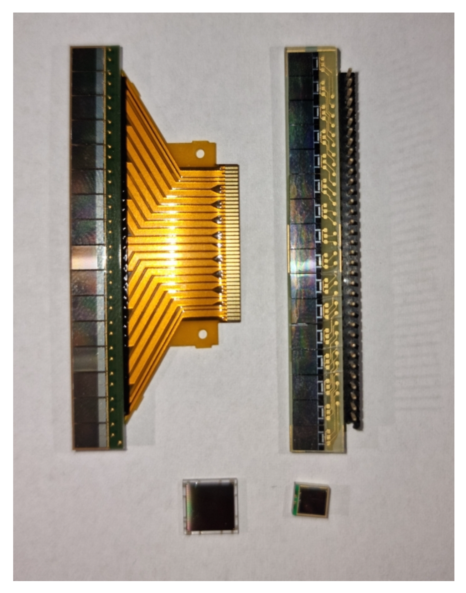
2.1. SiPM Sensors
- 1.
- Breakdown voltage refers to the voltage at which the silicon APDs within the SiPM enter Geiger mode, initiating the avalanche multiplication process. It is a critical parameter as it determines the operational voltage range of the SiPM and influences its sensitivity and noise characteristics. Because with the predecessor of SiPMs PMT used high voltage (thousands of Volts), the operating voltage is still called HV, although it is typically around 30–60 V.
- 2.
- Gain represents the amplification factor of the SiPM, indicating how many electron–hole pairs are generated per incident photon. It is typically expressed as the ratio of output charge (in photoelectrons) to input charge (number of incident photons).
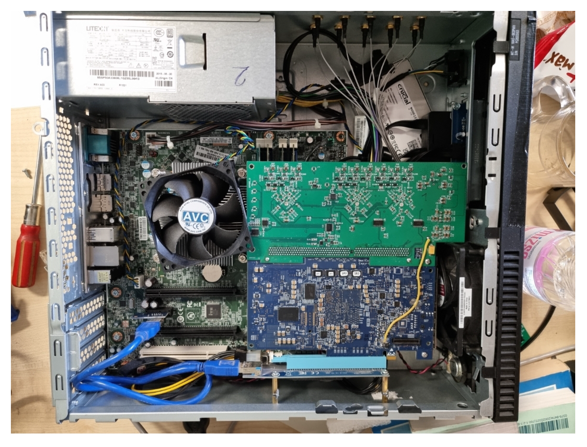
2.2. CMS BTL Tester
2.3. Backend
2.4. GUI
3. Measurements
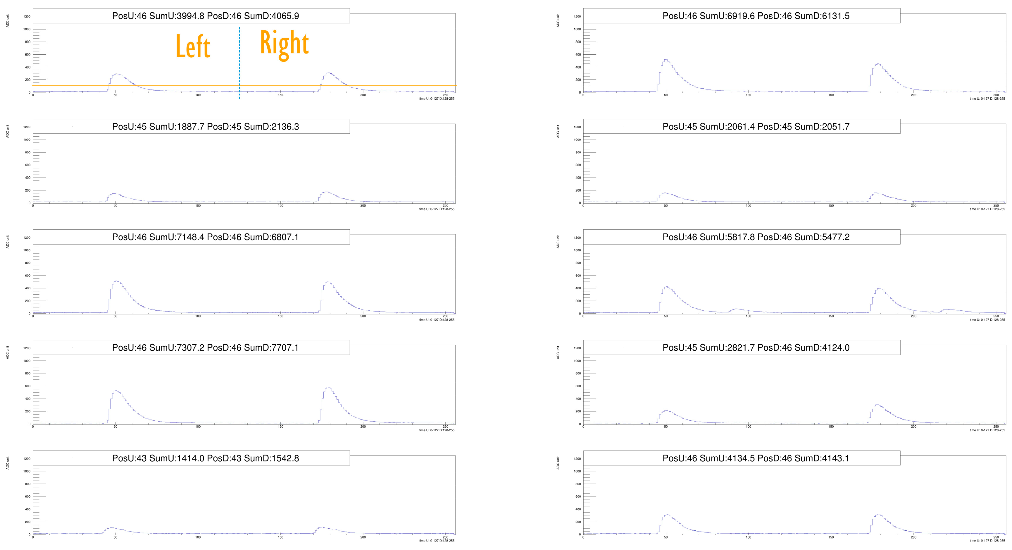
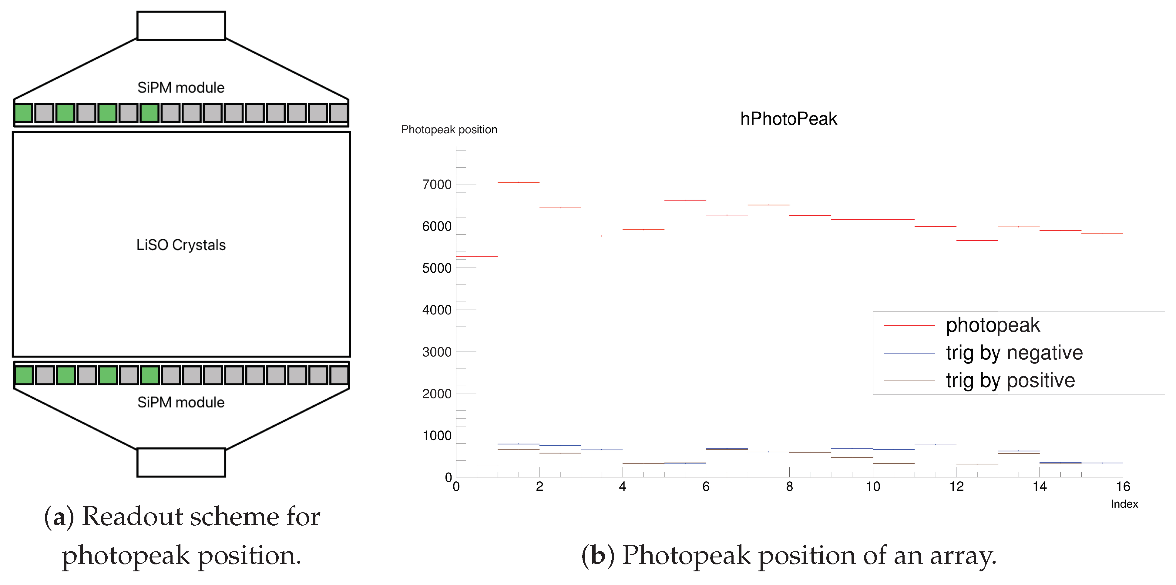
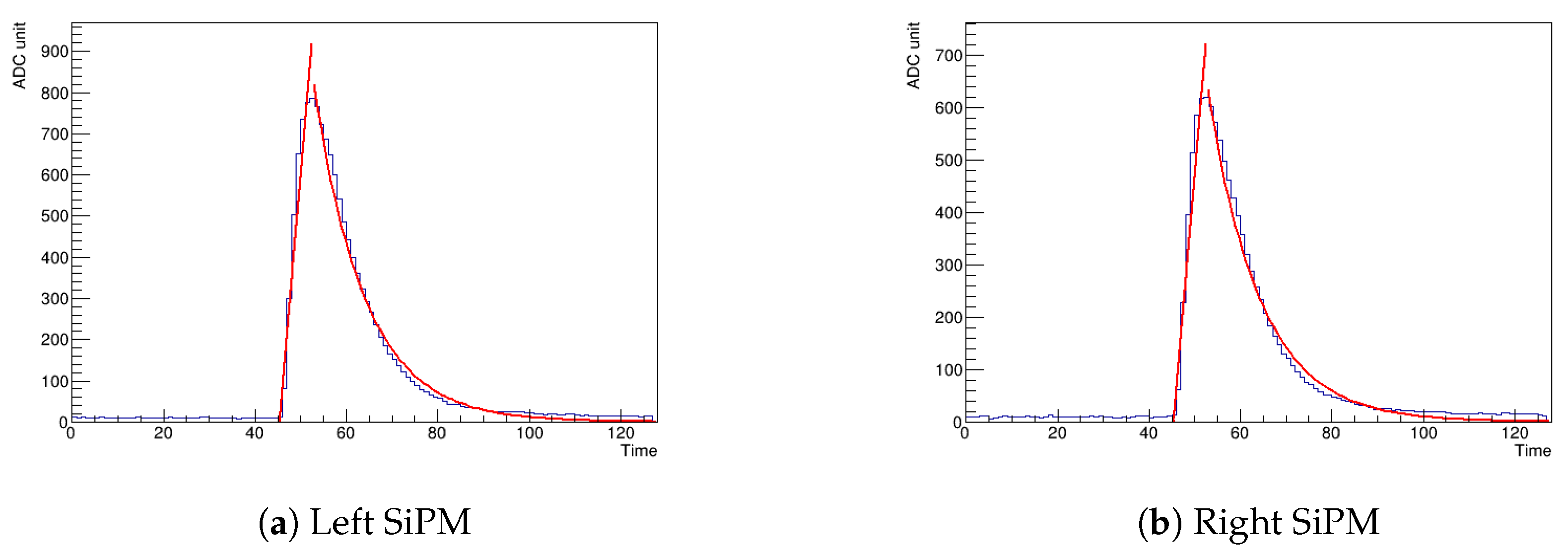
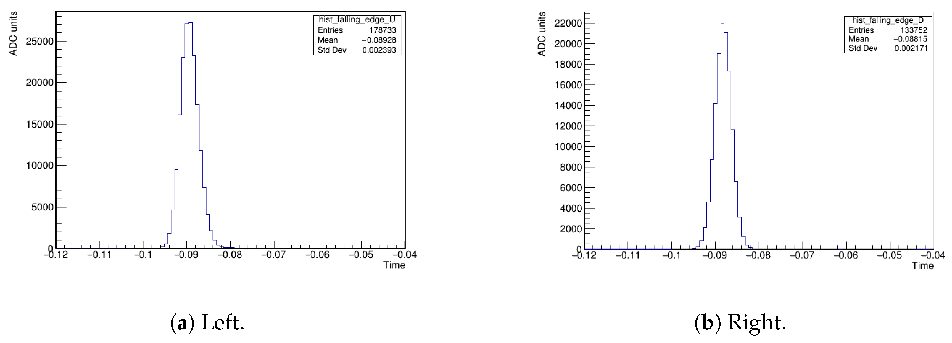
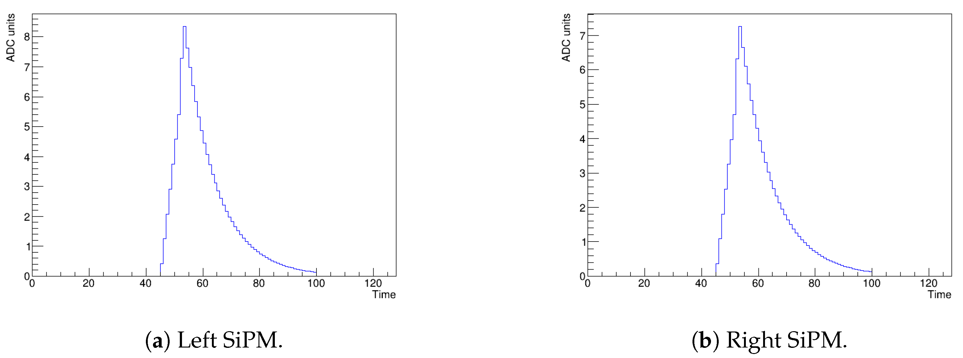
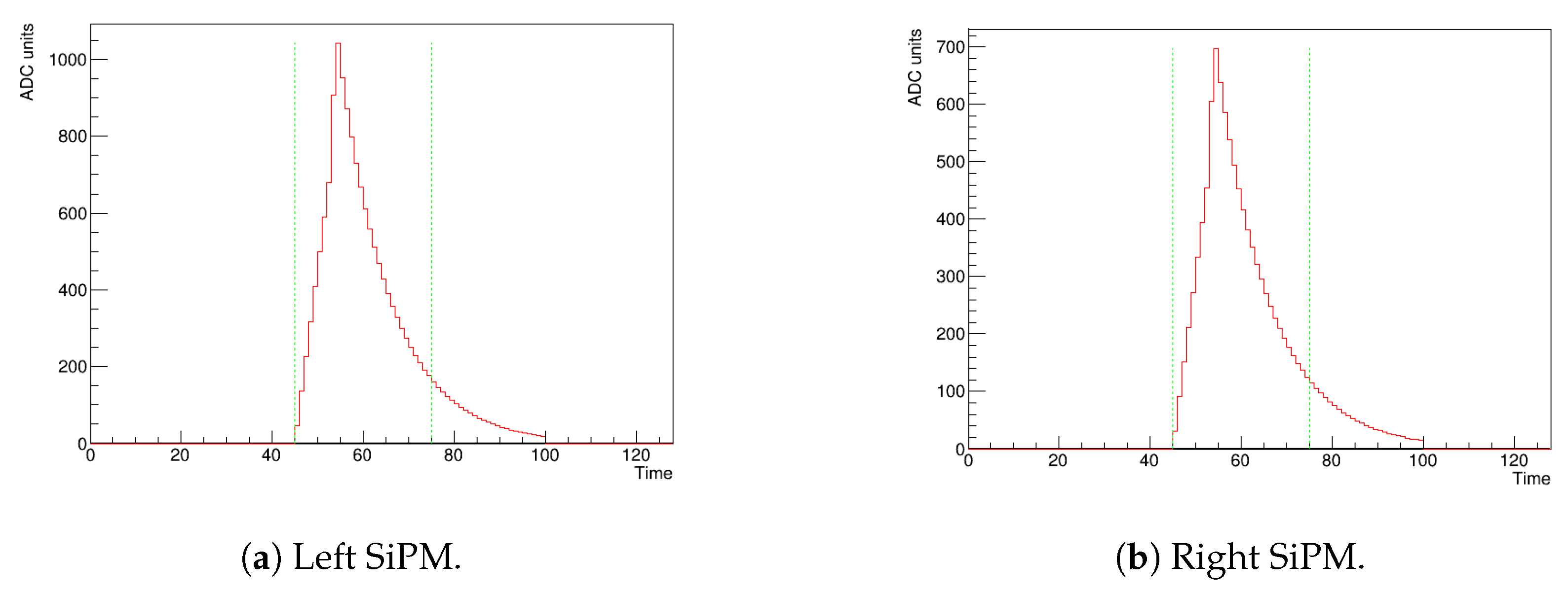
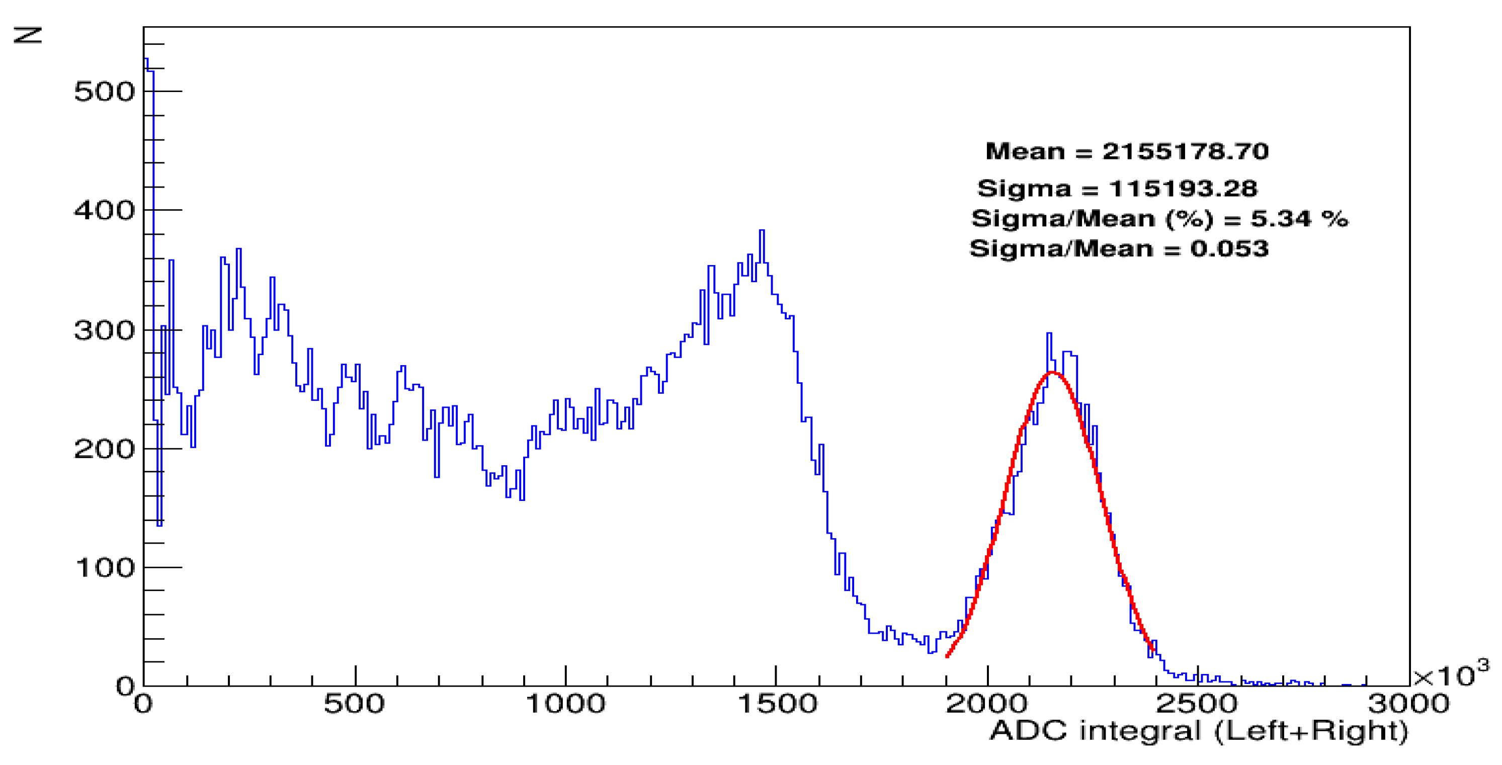
3.1. Photopeak Position
- 1.
- Different breakdown voltages and PDEs of the opposite sensors. A detailed test of the SiPMs is a must to minimise this differences.
- 2.
- Different geometries of the LYSO crystal are tested (https://indico.cern.ch/event/1091653/contributions/4592080/attachments/2347379/4003069/MTD_Poster.pdf (accessed on 31 July 2024)).
- 3.
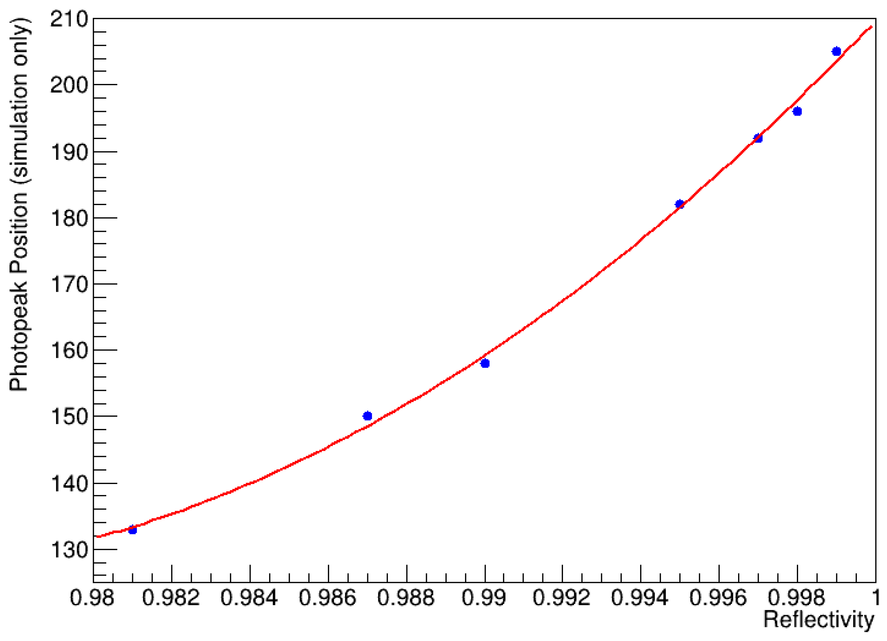
- The reflective index of the coating and quantity of the gluing can be estimated with this measurement and simulations.
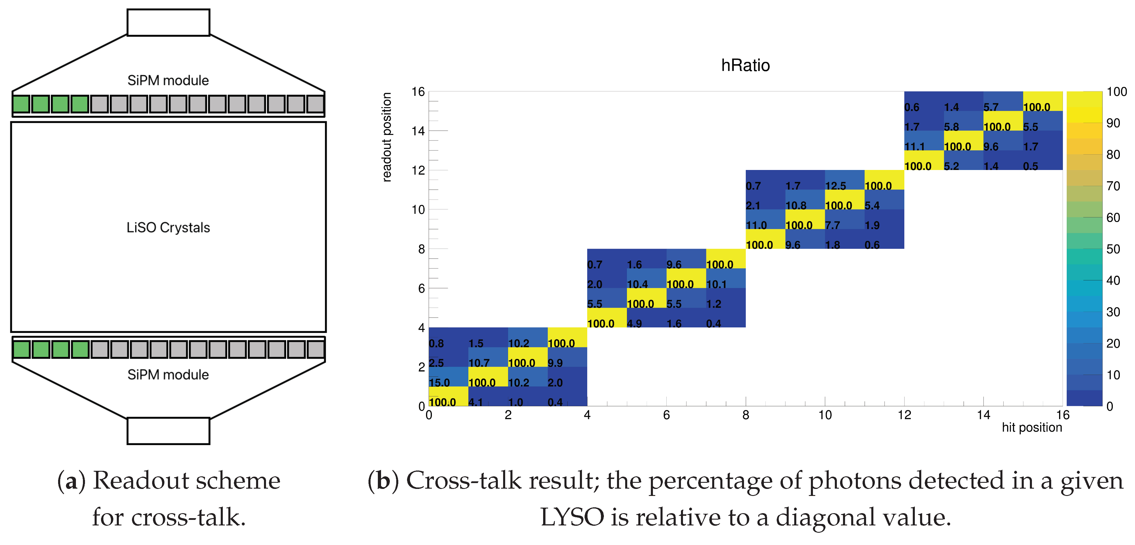
3.2. Optical Cross-Talk
4. GEANT4 Simulation of the Module
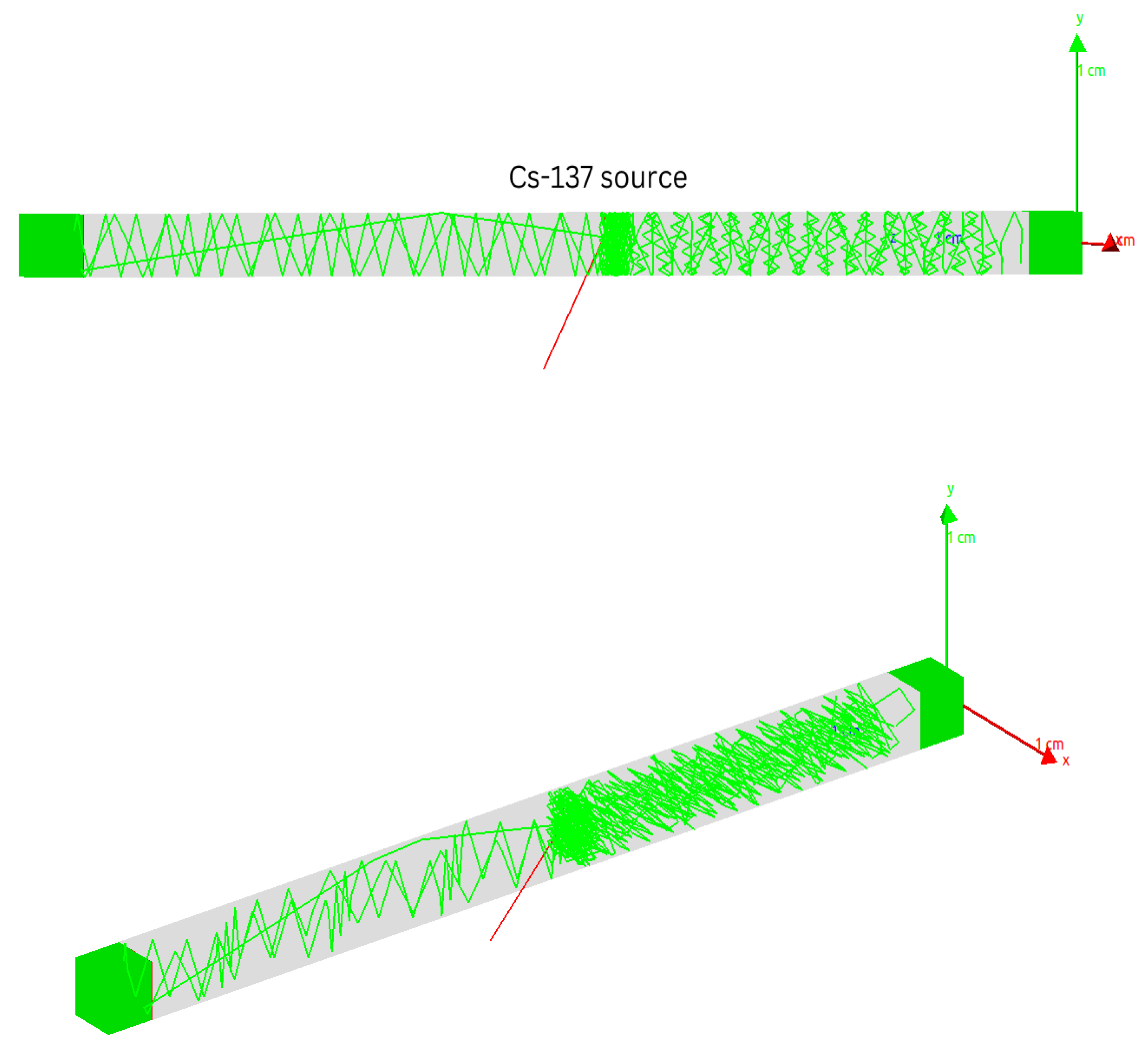
4.1. GEANT4 Simulation
4.2. Cs-137 Spectrum from Simulation
5. Discussion
Author Contributions
Funding
Data Availability Statement
Conflicts of Interest
Abbreviations
| ADC | Analog-to-Digital Converter |
| APD | Avalanche Photodiode |
| ASIC | Application-Specific Integrated Circuit |
| BGO | Bismuth Germanate |
| CERN | Conseil Européen pour la Recherche Nucléaire, European Organisation for Nuclear Research |
| DAQ | data acquisition |
| GEANT4 | Geometry ANd Tracking, CERN simulation framework for particle interaction |
| LIDAR | Light Detection And Ranging |
| LYSO | Lutetium Yttrium Oxyorthosilicate |
| MSPS | Megasamples Per Second |
| MRI | Magnetic Resonance Imaging |
| PCB | Printed Circuit Board |
| PET | Positron Emission Tomography |
| PMT | Photomultiplier Tube |
| PDE | Photon Detection Efficiency |
| SiPM | Silicon Photomultiplier |
| YSO | Yttrium OrthoSilicate |
| FPGA | Field-Programmable Gate Array |
References
- CMS Collaboration. A MIP Timing Detector for the CMS Phase-2 Upgrade. CERN Document Server. Available online: https://cds.cern.ch/record/2667167/files/CMS-TDR-020.pdf (accessed on 4 October 2023).
- Santanastasio, F. Precision Timing in the CMS MTD Barrel Timing Layer with Crystal Bars and SiPMs. IEEE Trans. Nucl. Sci. 2020, 67, 2105–2110. [Google Scholar] [CrossRef]
- Willeke, F.; Beebe-Wang, J. Electron Ion Collider Conceptual Design Report 2021; U.S. Department of Energy: Washington, DC, USA, 2021. [CrossRef]
- Khalek, R.A.; Accardi, A.; Adam, J.; Adamiak, D.; Akers, W.; Albaladejo, M.; Al-bataineh, A.; Alexeev, M.G.; Ameli, F.; Antonioli, P.; et al. Science Requirements and Detector Concepts for the Electron-Ion Collider: EIC Yellow Report. Nucl. Phys. A 2022, 1026, 122447. [Google Scholar] [CrossRef]
- CMS Collaboration. Phase 1 upgrade of the CMS Hadron Barrel Calorimeter. Nucl. Instrum. Methods Phys. Res. Sect. Accel. Spectrometers Detect. Assoc. Equip. 2022, 1042, 167389. [Google Scholar] [CrossRef]
- Yokoyama, M.; Minamino, A.; Gomi, S.; Ieki, K.; Nagai, N.; Nakaya, T.; Nitta, K.; Orme, D.; Otani, M.; Murakami, T.; et al. Performance of multi-pixel photon counters for the T2K near detectors. Nucl. Instrum. Methods Phys. Res. Sect. Accel. Spectrometers Detect. Assoc. Equip. 2010, 622, 567–573. [Google Scholar] [CrossRef]
- The CALICE Collaboration. Construction and commissioning of the CALICE analog hadron calorimeter prototype. Nucl. Instruments Methods Phys. Res. Sect. Accel. Spectrometers Detect. Assoc. Equip. 2019, 926, 85–100. [Google Scholar]
- Brun, R.; Rademakers, F.; Panacek, S. ROOT, an object oriented data analysis framework. Nucl. Instrum. Methods Phys. Res. A 1997, 389, 81–86. [Google Scholar] [CrossRef]
- Luxium Solutions. LYSO Scintillation Crystal. Available online: https://www.luxiumsolutions.com/radiation-detection-scintillators/crystal-scintillators/lyso-scintillation-crystals (accessed on 3 July 2024).
- GEANT4 Collaboration. GEANT4: A Simulation Toolkit. Available online: https://geant4.web.cern.ch (accessed on 3 July 2024).
- Agostinelli, S.; Allison, J.; Amako, K.; Apostolakis, J.; Araujo, H.; Arce, P.; Asai, M.; Axen, D.; Banerjee, S.; Barrand, G.; et al. Geant4—A simulation toolkit. Nucl. Instrum. Methods Phys. Res. A 2003, 506, 250–303. [Google Scholar] [CrossRef]
- Lucchini, M.; on behalf of the CMS Collaboration. Development of the CMS MIP timing detector. Nucl. Instrum. Methods Phys. Res. A 2020, 958, 162090. [Google Scholar] [CrossRef]


Disclaimer/Publisher’s Note: The statements, opinions and data contained in all publications are solely those of the individual author(s) and contributor(s) and not of MDPI and/or the editor(s). MDPI and/or the editor(s) disclaim responsibility for any injury to people or property resulting from any ideas, methods, instructions or products referred to in the content. |
© 2024 by the authors. Licensee MDPI, Basel, Switzerland. This article is an open access article distributed under the terms and conditions of the Creative Commons Attribution (CC BY) license (https://creativecommons.org/licenses/by/4.0/).
Share and Cite
Baranyai, D.; Oniga, S.; Gyongyosi, B.; Ujvari, B.; Mohamed, A. Module Tester for Positron Emission Tomography and Particle Physics. Electronics 2024, 13, 3066. https://doi.org/10.3390/electronics13153066
Baranyai D, Oniga S, Gyongyosi B, Ujvari B, Mohamed A. Module Tester for Positron Emission Tomography and Particle Physics. Electronics. 2024; 13(15):3066. https://doi.org/10.3390/electronics13153066
Chicago/Turabian StyleBaranyai, David, Stefan Oniga, Balazs Gyongyosi, Balazs Ujvari, and Attia Mohamed. 2024. "Module Tester for Positron Emission Tomography and Particle Physics" Electronics 13, no. 15: 3066. https://doi.org/10.3390/electronics13153066