Abstract
A novel Gm-C structure of a second-order continuous-time filter is proposed that allows for the independent control of the filter’s natural frequency (ω0) and quality factor (Q). The structure consists of two capacitors and four transconductors. Two transconductors together with the capacitors form a lossless second-order circuit with tunable ω0. The other two transconductors form a variable gain amplifier (VGA) which realizes an adjustable loss and thereby adjustable Q. The proposed solution can be used to implement low-voltage and low-power tunable front-end filter banks for fully integrated CMOS cochlear implants and edge intelligence accelerators. An example filter bank powered by 0.5 V and consuming 40 nW of power per single filter is designed and simulated using a 180 nm CMOS process. Circuitries for the adaptive control of transistor bias at a reduced supply voltage are proposed. The ω0 and Q control circuitries are also proposed: a delay-locked loop (DLL)-based system for fine ω0 tuning and a binary-weighted current mirror for Q adjustment. The proposed solution allows for the independent regulation of ω0 and Q within the ranges of 0.25–8 kHz and 1–14, respectively, with a relative tolerance of up to 5% across a filter bank.
1. Introduction
The natural auditory process takes place, in simple words, in three stages: the conversion of a mechanical sound wave to an electrical signal, the decomposition of the wide sound spectrum to narrower bands, and neural processing [1]. This natural scheme is energy- and computationally efficient and is exploited in bio-inspired electronic devices such as hearing aids, cochlear prosthesis implants [2,3,4,5,6,7], and edge AI accelerators [8,9,10,11,12,13,14]. In these devices, the sound wave is converted to a voltage signal by a MEMS transducer and then applied to a set of band-selective filters which divide the sound spectrum into a number of adjacent channels. The channel signals are then shaped and converted into pulses that stimulate the patient’s auditory nerves or drive artificial neural networks in edge devices.
The filter set, referred to as a filter bank, typically contains up to sixteen filters with different frequency and selectivity [15,16]. The parameters are set individually to each filter in a bank depending on the content and dynamics of sound, patient characteristics, etc. Commercial solutions widely use digital filters because their characteristics are practically insensitive to process, voltage, and temperature (PVT) variations. However, research on analog filter banks is still being carried out worldwide [5,6,7,9,10,11,12,13,14,17,18,19,20,21,22,23,24], and in recent years, several solutions have been reported with very competitive performance in terms of power consumption, e.g., [9,10,11,12,13,14]. Thus, analog filters can be energy-efficient, but their limited tunability, relatively high sensitivity to technological imperfections, and limited dynamics at low supply voltage are still a challenge for designers. A supply voltage of, e.g., 0.5–0.6 V [7,10,11,19,22] means in practice that MOS transistors are biased slightly above the triode region. As a consequence, the transistor output resistance is reduced, which limits a filter selectivity (a filter quality factor). Thus, at low supply voltages, additional control circuits are necessary to prevent the transistors from entering the triode region. The tunability problem is related to the fact that known topologies of continuous-time filters [23] feature a not fully independent (separated) control of the filter frequency and quality factor [24]. This fact complicates the tuning of a whole filter bank and makes it more difficult to control the filter characteristics under PVT variations.
The continuous-time filter presented in this paper addresses the requirements of full tunability and low-voltage operation. The solution exploits the new proposed Gm-C schematic of a biquadratic filter with the separate control of the natural frequency (ω0) and quality (Q) factor. The following sections present the concept, theoretical analysis, transistor-level schematic, and simulation results of the filter designed in the X-Fab 180 nm CMOS process, together with a DLL-based frequency tuning system and circuits controlling the bias and threshold voltage of transistors. An example filter bank is also presented.
2. Filter
Figure 1a shows the Gm-C topology of the proposed filter. The transconductance amplifiers Gm1 and Gm2 together with the capacitors C1 and C2 are a second-order, lowpass, and lossless circuit with a natural (resonance) frequency ω0 [24]. The loss is introduced to the circuit by a negative feedback loop established on the transconductors Gm3 and Gm4.
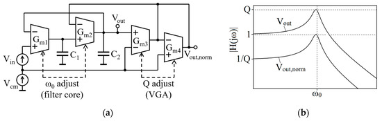
Figure 1.
Proposed lowpass filter: (a) Gm-C topology; (b) typical amplitude characteristic (the vertical scale is logarithmic).
The input AC voltage Vin is applied to the filter with respect to a common (DC) potential Vcm. The filter’s main output terminal is Vout. The filter’s AC transmittance is
where
To simplify the filter design, Gm1 and Gm2 as well as C1 and C2 can be assumed to be equal, i.e., Gm1 = Gm2 = Gm1,2, and C1 = C2 = C1,2. With these assumptions, (2) simplifies to
The CMOS realization of the Gm-C structure is shown in Figure 2a. The transconductors have an identical topology composed of a differential pair (M1, M2) loaded with a current mirror (M3, M4). The consecutive differential pairs are biased with the currents IB1 to IB4 generated by the transistors MB1 to MB4. The transistors M5, M6, and additional capacitors of 20 pF over M5 compose the DC voltage shifters to increase the drain-source voltage of the M2 transistors [23].
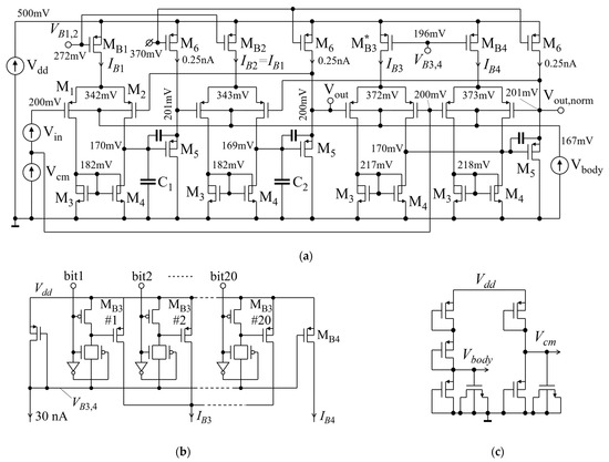
Figure 2.
The CMOS realization of the filter: (a) electrical diagram; (b) programmable current mirror generating IB3 and IB4; and (c) the generator of Vcm and Vbody. The node voltage values are with IB1 = IB2 = 10 nA, IB3 = IB4 = 30 nA, and temperature 27 °C.
The transconductance of the i-th (i = 1…4) transconductor, Gmi, is equal to the transconductance of the transistors M1 and M2 (gm1 = gm2 = gm1,2) in the respective differential pair, i.e., Gmi = (gm1,2)i. M1 and M2 operate in saturation and weak inversion regions; thus,
where i = 1…4, Vt = kT/q is the thermal voltage, and n is a technology-dependent parameter [21,22].
The bias currents IB1 and IB2 are equal (IB1 = IB2 = IB1,2), so the natural frequency and quality factor of the filter can be expressed as follows
As indicated by (5), Q is determined by the ratio of the bias currents IB4 and IB3. Therefore, Q can be adjusted by means of a scalable (programmable) current mirror shown in Figure 2b where a current ratio, once programmed, does not change with PVT. However, ω0 depends on the absolute values of the parameters IB1,2, n, and Vt, so it varies with process and temperature, and thus, a tuning system based on a PLL or DLL is necessary.
It is worth noting that the filter operates in a unity gain buffer configuration [25]. The filter is covered with a global negative feedback loop (established by connecting a Vout terminal to an inverting input of the amplifier Gm1), which forces Vout to follow Vin at low frequencies. As a result, the filter gain at low frequencies is 1 V/V regardless of mismatch and PVT variations. Note also that at the additional output, Vout,norm, the filter peak gain is unity, as the graph in Figure 1b shows.
The detailed data on the transistor sizes and bias conditions are given in Table 1.

Table 1.
DC operating point simulated at the following: Vdd = 0.5 V, Vcm = 0.4Vdd, Vbody = Vdd/3, IB1 = IB2 = 10 nA, IB3 = IB4 = 30 nA, and T = 27 °C. Nominal corner.
2.1. Effect of Reduced Resistance
With a Vdd of 0.5 V, the transistor drain-source voltages (VDS) are significantly reduced, so they are only slightly above saturation voltages (VDSsat). According to detailed data in Table 1, the saturation margin |VDS| − |VDSsat| is 80–150 mV across all transistors. The low VDS voltages result in the reduced output resistance (rds) of the transistors. E.g., the output resistance of M2 is rds2 = 980 MΩ at VDS = 170 mV and would be 1.5 GΩ when assuming VDS = 270 mV. The reduced transistor resistance causes the actual Q value to be smaller than its ideal value given by (3).
Including the output resistances, the actual ω0 and Q are
where Ro1,2 = Ro1 = Ro2 = rds2 ‖ rds4 is the output resistance of the transconductors Gm1 and Gm2, and k is the voltage gain of the VGA,
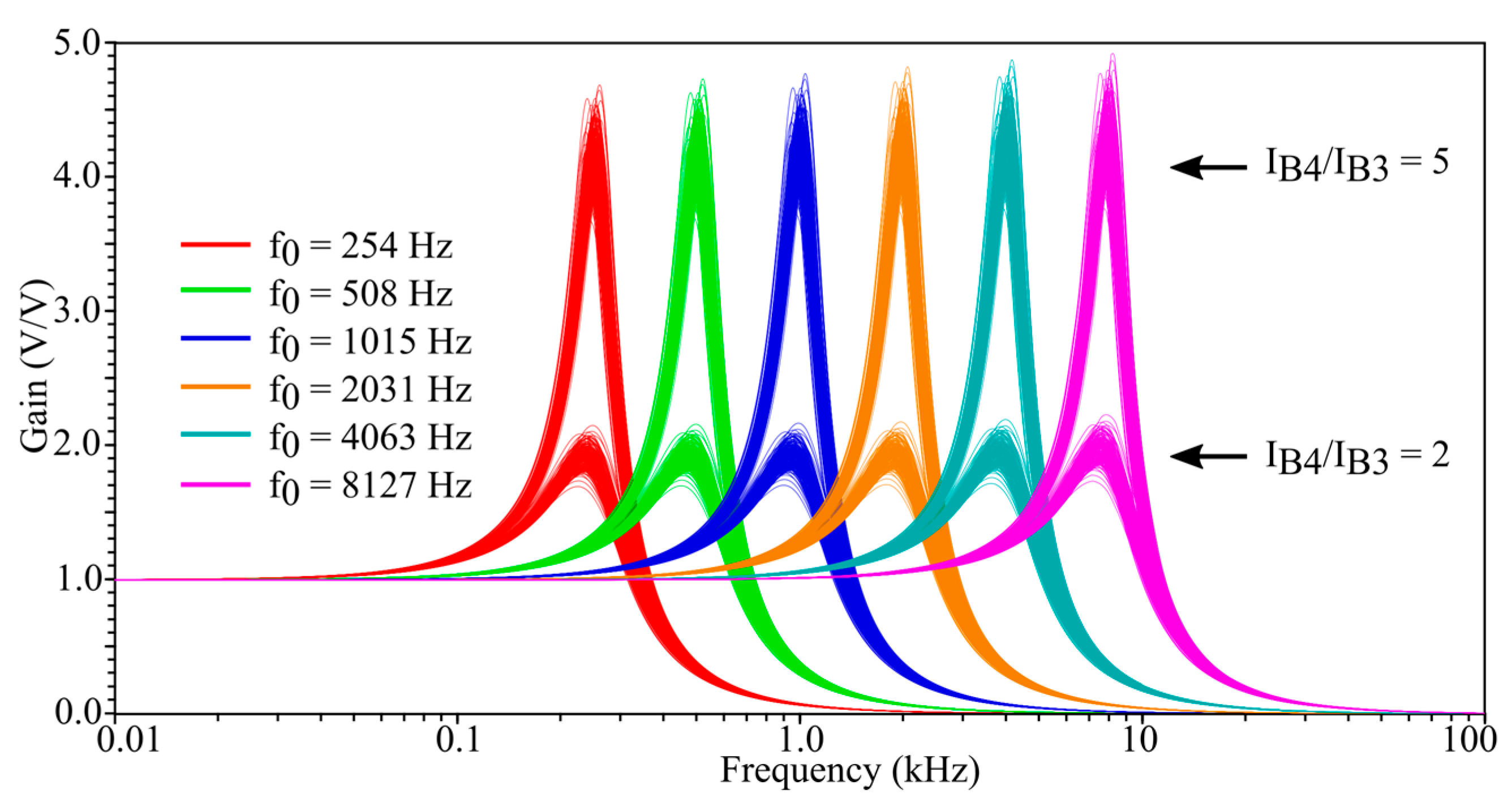
Since the transconductor’s gain (Gm1,2Ro1,2) remains approximately constant and equal to Gm1,2Ro1,2 ≈ 100 over a wide range of IB1,2, the actual ω0 is practically equal to its ideal value (3), as indicated by (6). On the other hand, the finite Gm1,2Ro1,2 ≈ 100 reduces Q by 10–30% with respect to its ideal value (3), i.e., Qactual = 0.7(Gm4/Gm3) for high Q values, and Qactual = 0.9(Gm4/Gm3) for low Q. Figure 3 presents the simulated filter characteristics where IB1,2 is set to 5, 10, and 20 nA (the ω0 adjustment), and IB4/IB3 is programmed as 2, 4, 10, and 20 (the Q adjustment). The resulting Q values are reduced by 15–35% with respect to the IB4/IB3 ratios, which is caused by the reduced resistances, as mentioned, and in addition by the inequality Gm4/Gm3 ≅ IB4/IB3. However, the Q values are well repeatable at different ω0.
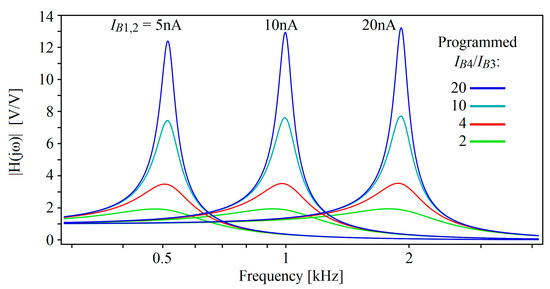
Figure 3.
Simulation of ω0 and Q adjustments. Nominal corner. C1,2 = 24 pF. T = 27 °C.
2.2. Bias and Threshold Voltage Control
Due to the low supply voltage, the threshold voltages of the selected transistors are reduced using the body effect. Thus, the bodies of the n-channel devices (M3, M4) are connected to the higher potentials at their gates (n-channel transistors on insulated p-wells, available in the X-Fab process, are used). The bodies of the p-channel pairs (M1, M2) are connected to the low reference potential Vbody. The Vbody is regulated depending on the supply voltages Vdd to prevent the forward biasing of the body-source (p-n) junctions in M1 and M2. The common potential Vcm is also regulated so that the transistor drain-source voltages (VDS) are maximized. The simple and effective control scheme with Vbody = Vdd/3 and Vcm = 0.4∙Vdd is used in this design. The Vcm and Vbody are generated by the active dividers, shown in Figure 2c, that have simple topology and are immune to PVT variations. With this adaptive bias, the transistors are kept in saturation for a wide range of Vdd, from 1.8 V down to 0.4 V. Unfortunately, the simple dividers in Figure 2c transmit AC noise from the Vdd line to the Vbody and Vcm lines, which reduces the power supply rejection ratio (PSRR) of the entire filter. However, additional grounded capacitors connected to the Vbody and Vcm lines effectively reduce the Vdd noise. Simulations show that the additional capacitors of about 25 pF result in a PSRR of 72 dB and 51 dB at 10 Hz and 1 kHz, respectively (the mismatch of the differential pairs and current mirrors was included in the PSSR simulations). The grounded capacitors can be made from n-channel transistors, as shown in Figure 2c.
3. Frequency Tuning System
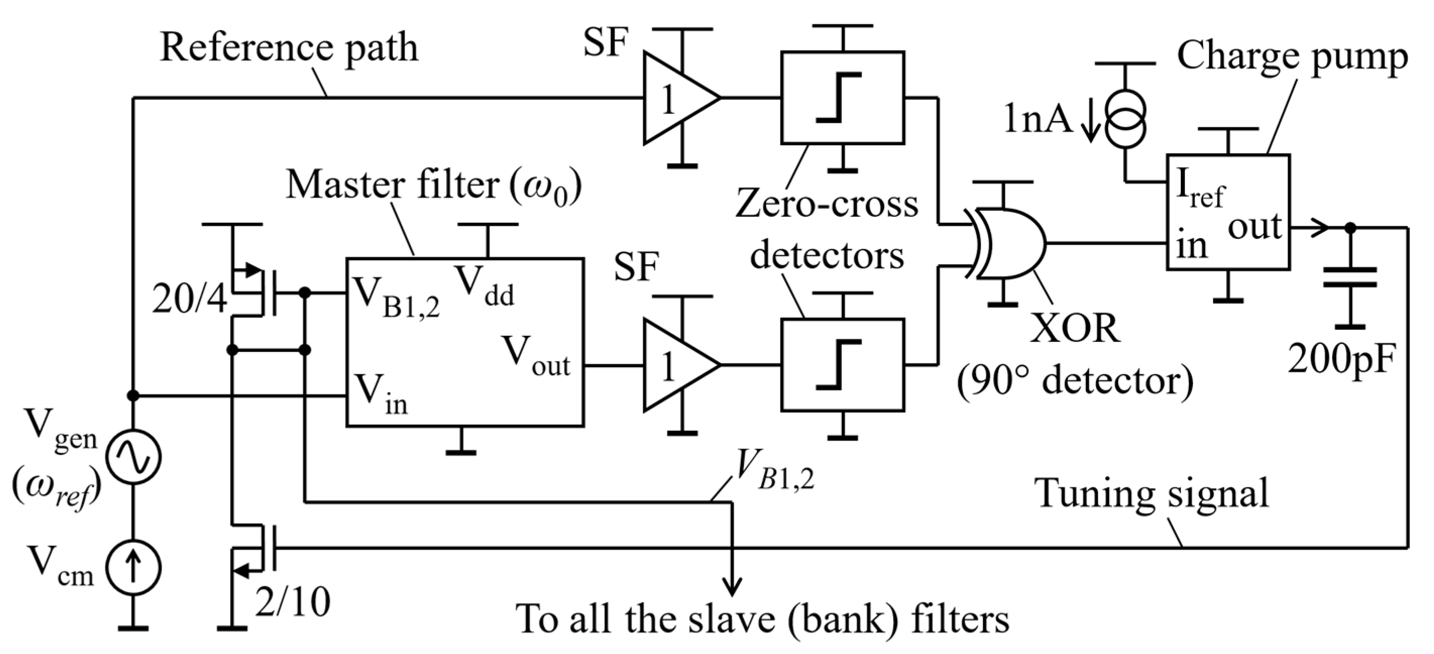
Due to PVT variations, continuous-time filters require an automatic frequency tuning system. The most common way to tune Gm-C filters is through a master–slave structure [26,27,28,29,30]. This approach requires a good match between master and slave circuits. To achieve the best match, the proposed tuning system, shown in Figure 4, uses a copy of one of the filters from the filter bank as the master circuit.
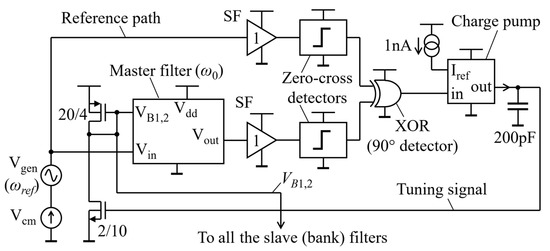
Figure 4.
DLL-based tuning system.
The system in Figure 4 is a typical delay-locked loop which utilizes the fact that biquadratic lowpass filters have a phase shift of −90° (−π/2) at ω0. Thus, the reference sine signal (Vgen) with a frequency of ωgen is transmitted along two paths: the reference and filter paths. If the signal after passing through the (master) filter is delayed exactly by 90° with respect to the reference path, this means that the natural frequency of the (master) filter is equal to the reference frequency, i.e., ω0 = ωgen. If the 90° shift remains constant, then the XOR gate generates a square wave with a constant duty cycle of exactly 50%. As a result, the charge pump equally charges and discharges its capacitor, and consequently, a voltage on the tuning signal line remains constant.
The amplitude of the input reference sine is limited by the dynamics of the filter and is Vgen = 20–50 mVpp for the filter with Q = 1 and Vdd = 0.5 V. The phase detector, based on a simple digital XOR gate, requires high amplitude signals. Therefore, weak sine signals are amplified by the zero-cross detectors, which convert them to square waves with a rail-to-rail amplitude. The correct system operation requires the cross-detectors to be insensitive to the DC levels at their inputs. Thus, a solution with a decoupling capacitor is used [29], whose schematic is shown in Figure 5a. Other sub-blocks of the tuning system are depicted in Figure 5b–d.
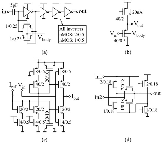
Figure 5.
The sub-circuits of the tuning system: (a) zero-cross detector; (b) source follower (SF); (c) charge pump; and (d) XOR gate. The transistor body terminals not shown are connected to the Vdd (PMOS) and ground (NMOS) potentials, respectively.
The source followers (SFs) use p-channel transistors biased with 20 nA currents (Figure 5b). The SFs have their threshold voltages reduced by means of the body effect (Vbody), resulting in a gain that is not unity. However, both SFs are identical, and therefore, their non-unity gain does not affect the phase shift detection process. The charge pump (Figure 5c) is a bidirectional current source (Iout) controlled by voltage (Vin). Thus, Iout = Iref at Vin = L (low state), and Iout = −Iref at Vin = H (high state). Additional capacitors, made of transistors 20 µm wide and 10 µm long (20/10), reduce glitches in the output current caused by commutation. The XOR gate (Figure 5d) is a traditional low-voltage solution with a transmission gate. The transistor body terminals not shown explicitly in the schematics in Figure 5a–d are connected to the Vdd and ground potentials for the p- and n-channel transistors, respectively.
All sub-blocks of the tuning system, including the master filter, operate with the same supply voltage, Vdd = 0.5 V. Assuming an external reference generator, the power consumption of the tuning system is 80 nW, and the occupied silicon area is smaller than two filters in a filter bank.
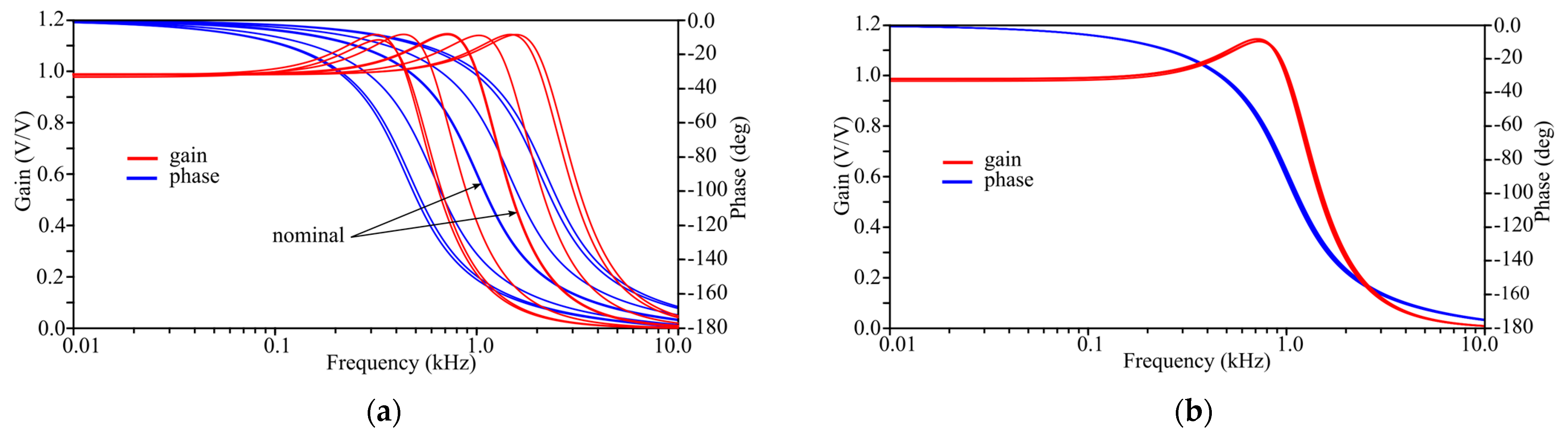
The master filter is the filter of Figure 2 with C1,2 = 24 pF and Q = 1. In the ideal case, i.e., no PVT variations, the natural frequency of the master filter is ω0 = 1 kHz at IB1,2 = 10 nA and T = 27 °C, as shown in Figure 3. Under PVT variations, the ω0 changes substantially, from about 400 Hz to 1.2 kHz (changes in the filter quality factor are negligible), as shown in Figure 6a where the following variations are assumed: (P)process across five typical corners, supply (V)voltage from 450 to 550 mV, and (T)temperature from 0 to 50 °C. The tuning system with ωgen = 1 kHz effectively stabilizes the filter characteristics. The resulting ω0 deviates by ±2% from 1 kHz, as visible in Figure 6b (note that the tuning system is also under PVT variations).

Figure 6.
The master filter characteristics simulated under PVT variations: (a) without tuning and (b) with the tuning system. The process variation is simulated in 5 corners: tm, wp, ws, wo, and wz. (Supply) Voltage variation: 0.5 V ± 50 mV. Temperature variation: 0, 27, and 50 °C.
4. Filter Bank
Table 2 shows an example of 16 filters scaled from 250 Hz to 8 kHz.
Table 2.
Filter bank example.
The bias current IB1,2 can be the same for all channels, which simplifies the biasing, scaling, and tuning of the entire bank. The frequencies of the individual channels are then obtained simply by scaling the capacitance C1,2. Thanks to this, relations between the channels’ frequencies are relatively lowly sensitive to PVT variations. Mismatch, though, affects the bank characteristics, as shown in Figure 7 (for better visualization, six filters selected of the sixteen are plotted). The 1-sigma spreads in ω0 and Q are 2.2% and 4.4%, respectively, across the entire bank.
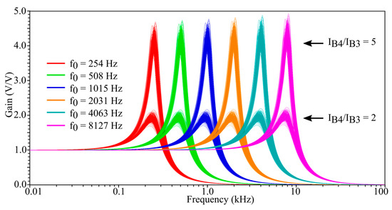
Figure 7.
The filter bank simulated under mismatch (500 Monte Carlo runs).
The power consumption of the whole bank depends on the programmed value of Q. Assuming the same Q in all channels, the 16-filter bank consumes 16∙27 = 432 nW at Q = 10 and 16∙40 = 640 nW at Q = 1. The lower power consumption can be achieved by reducing the filter bias currents. Unfortunately, lower currents mean larger mismatches between transistor transconductances [31,32] and thus greater spreads in ω0 and Q.
The typical noise of the individual filter is 18–33 µVRMS, when referred to the filter input and integrated over the filter band. The total harmonic distortion (THD) parameter is 1% with the input sine excitation with an amplitude of 72 mVRMS and a frequency of ω0/5. The 1 dB input-referred compression point is –13.82 dBm (45.5 mVRMS) with the excitation at a frequency close to ω0. Thus, the filter dynamics are 66 dB and 62 dB regarding the 1% THD and 1 dB compression point, respectively.
The silicon area occupied by the filters is determined by the area of their capacitors [22,24,25]. E.g., the filter with ω0 = 1.015 kHz contains two capacitors of 23.48 pF and additionally, three capacitors at M5 transistors of 20 pF, each. Assuming typical double MIM capacitors of 2.2 fF/µm2, the filter area is 48,500 µm2 (221 µm × 221 µm). However, using triple-high-capacitance MIMs of 7 fF/µm2, also available in the X-Fab process, the filter area reduces threefold, to 15,300 µm2 (124 µm × 124 µm).
5. Discussion
Table 3 presents a brief review of the continuous-time filters for auditory and edge devices, published across the last decade. Edge devices typically need filters with a constant Q parameter of low value, e.g., Q = 1.3 [19] or Q = 2 [10,11,20]. Filters with a fixed Q can have simplified, transistorized topology and therefore consume relatively low power, even several nanowatts per a whole filter bank [11]. On the other hand, cochlear implants require filters with precisely controlled frequency, bandwidth, and gain, due to individual patient characteristics [5,7,17,22]. Thus, cochlea-intended filters have more complicated topology and higher power consumption compared to edge filters.
Table 3.
Continuous-time filter banks published in the last ten years.
The filter proposed in this work consumes less power than the other cochlea-dedicated filters [5,7,17,22] but still more compared to the simple filters in the edge accelerators [10,11,19,20]. Most of the filter power (75%) is dissipated in the VGA used to adjust Q. Assuming a fixed Q, e.g., 2, the VGA is not needed, and thus, the power of the filter bank can be reduced from 640 nW to 170 nW.
To reduce power consumption, supply voltages of filter banks are reduced when compared to the nominal voltages specified for the CMOS processes in which the filter banks were made. E.g., the filter bank of [20] was developed in a 3.3 V process and is supplied with a 2.5 V voltage. Similarly, the filters developed in 1.8 V processes operate at a supply voltage reduced to 1 V [5], 0.6 V [10], and 0.5 V [7,22], [this work]. Also, the works [19] and [11], made in 1 V processes, use 0.5 and 0.6 V supplies, respectively. In this regard, a typical practical limit of an analog filter supply voltage is about 0.5 V considering many CMOS processes. This practical limit applies to the analog continuous-time filters as well as discrete-time, switched-capacitor ones [12,13,14] (not included in Table 3). A further reduction in a supply voltage is, however, possible through a further reduction in transistor threshold voltages, to below 200 mV. Unfortunately, a significant increase in mismatch and noise is observed at such low threshold voltages, so more sophisticated bias control and tuning systems, based on digital circuits, are required.
6. Conclusions
The novel transconductance-C structure of a lowpass second-order filter with the separate control of the natural frequency and quality factor was proposed. The feasibility of implementing the proposed filter structure in 180 nm X-Fab CMOS technology at a significantly reduced supply voltage was investigated. The advantage of this technology, i.e., the ability to control the body potentials of both p-channel and n-channel transistors (and thus the ability to reduce and control the threshold voltages in both types of transistors), was exploited in order to achieve an optimal operating point at a 0.5 V supply. The impacts of the supply voltage noise, temperature changes, and technological imperfections on the filter’s performance were carefully analyzed. A low-voltage tuning system with a phase detector to stabilize the filter natural frequency was also proposed.
Author Contributions
W.J. and J.J. contributed equally to conceptualization, methodology, formal analysis, simulations, writing—original draft preparation, and writing—review and editing. All authors have read and agreed to the published version of the manuscript.
Funding
This research received no external funding.
Data Availability Statement
Data are contained within this article.
Conflicts of Interest
The authors declare no conflicts of interest.
References
- Russo, M.; Stella, M.; Sikora, M.; Pekić, V. Robust Cochlear-Model-Based Speech Recognition. Computers 2019, 8, 5. [Google Scholar] [CrossRef]
- Ahn, W.; Kim, D.; Park, J.; Park, J.H.; Lee, T.; Jeong, K.; Min, K.S.; Lee, H.; Je, M. A Reconfigurable Neural Stimulation IC with a High-Resolution Strength Control and In-Situ Neural Recording Function for Cochlear Implant Systems. IEEE Solid-State Circuits Lett. 2022, 5, 162–165. [Google Scholar] [CrossRef]
- Karrenbauer, J.; Klein, S.; Schönewald, S.; Gerlach, L.; Blawat, M.; Benndorf, J.; Blume, H. SmartHeaP—A High-level Programmable, Low Power, and Mixed-Signal Hearing Aid SoC in 22 nm FD-SOI. In Proceedings of the 48th IEEE European Solid State Circuits Conference, ESSCIRC 2022, Milan, Italy, 19–22 September 2022; pp. 265–268. [Google Scholar] [CrossRef]
- Yip, M.; Jin, R.; Nakajima, H.H.; Stankovic, K.M.; Chandrakasan, A.P. A Fully-Implantable Cochlear Implant SoC with Piezoelectric Middle-Ear Sensor and Arbitrary Waveform Neural Stimulation. IEEE J. Solid-State Circuits 2015, 50, 214–229. [Google Scholar] [CrossRef] [PubMed]
- Özbek, B.; Külah, H. A 1-V Nanopower Highly Tunable Biquadratic Gm−C Bandpass Filter for Fully Implantable Cochlear Implants. In Proceedings of the 2021 IEEE Biomedical Circuits and Systems Conference, BioCAS, Berlin, Germany, 7–9 October 2021; pp. 1–5. [Google Scholar] [CrossRef]
- Özbek, B.; Külah, H. A 9.03 µW Low Noise Highly Tunable Analog Front-End for Fully Implantable Cochlear Prosthesis. In Proceedings of the 2022 IEEE Biomedical Circuits and Systems Conference, BioCAS 2022, Taipei, Taiwan, 13–15 October 2022; pp. 349–353. [Google Scholar] [CrossRef]
- Yang, M.; Chien, C.-H.; Delbruck, T.; Liu, S.-C. A 0.5 V 55 μW 64 × 2 Channel Binaural Silicon Cochlea for Event-Driven Stereo-Audio Sensing. IEEE J. Solid-State Circuits 2016, 51, 2554–2569. [Google Scholar] [CrossRef]
- Shan, W.; Yang, M.; Xu, J.; Lu, Y.; Zhang, S.; Wang, T.; Yang, J.; Shi, L.; Seok, M. A 510nW 0.41V Low-Memory Low-Computation Keyword-Spotting Chip Using Serial FFT-Based MFCC and Binarized Depthwise Separable Convolutional Neural Network in 28 nm CMOS. In Proceedings of the 2020 IEEE International Solid-State Circuits Conference, ISSCC 2022, San Francisco, CA, USA, 16–20 February 2020; pp. 230–232. [Google Scholar] [CrossRef]
- Kim, K.; Gao, C.; Graça, R.; Kiselev, I.; Yoo, H.J.; Delbruck, T.; Liu, S.C. A 23μW Solar-Powered Keyword-Spotting ASIC with Ring-Oscillator-Based Time-Domain Feature Extraction. In Proceedings of the 2022 IEEE International Solid-State Circuits Conference, ISSCC 2022, San Francisco, CA, USA, 20–26 February 2022; pp. 1–3. [Google Scholar] [CrossRef]
- Yang, M.; Yeh, C.H.; Zhou, Y.; Cerqueira, J.P.; Lazar, A.A.; Seok, M. Design of an always-on deep neural network-based 1 µW voice activity detector aided with a customized software model for analog feature extraction. IEEE J. Solid-State Circuits 2019, 54, 1764–1777. [Google Scholar] [CrossRef]
- Yang, M.; Liu, H.; Shan, W.; Zhang, J.; Kiselev, I.; Kim, S.J.; Enz, C.; Seok, M. Nanowatt acoustic inference sensing exploiting nonlinear analog feature extraction. IEEE J. Solid-State Circuits 2021, 56, 3123–3133. [Google Scholar] [CrossRef]
- Zhang, S.; Su, F.; Wang, Y.; Mai, S.; Pun, K.P.; Tang, X. A Low-Power Keyword Spotting System with High-Order Passive Switched-Capacitor Bandpass Filters for Analog-MFCC Feature Extraction. IEEE Trans. Circuits Syst. I Reg. Pap. 2023, 70, 4235–4248. [Google Scholar] [CrossRef]
- Shi, E.; Tang, X.; Pun, K.P. A 270 nW switched-capacitor acoustic feature extractor for always-on voice activity detection. IEEE Trans. Circuits Syst. I Reg. Pap. 2021, 68, 1045–1054. [Google Scholar] [CrossRef]
- Villamizar, D.A.; Muratore, D.G.; Wieser, J.B.; Murmann, B. An 800 nW switched-capacitor feature extraction filterbank for sound classification. IEEE Trans. Circuits Syst. I Reg. Pap. 2021, 68, 1578–1588. [Google Scholar] [CrossRef]
- Wei, Y.; Ma, T.; Ho, B.K.; Lian, Y. The Design of Low-Power 16-Band Nonuniform Filter Bank for Hearing Aids. IEEE Trans. Biomed. Circuits Syst. 2019, 13, 112–123. [Google Scholar] [CrossRef]
- Cosentino, S.; Falk, T.H.; McAlpine, D.; Marquardt, T. Cochlear Implant Filterbank Design and Optimization: A Simulation Study. IEEE/ACM Trans. Audio Speech Lang. Process. 2014, 22, 347–353. [Google Scholar] [CrossRef]
- Liu, S.-C.; van Schaik, A.; Minch, B.A.; Delbruck, T. Asynchronous binaural spatial audition sensor with 2 × 64 × 4 channel output. IEEE Trans. Biomed. Circuits Syst. 2014, 8, 453–464. [Google Scholar] [CrossRef] [PubMed]
- Wang, S.; Koickal, T.J.; Hamilton, A.; Cheung, R.; Smith, L.S. A bio-realistic analog CMOS cochlea filter with high tunability and ultra-steep roll-off. IEEE Trans. Biomed. Circuits Syst. 2015, 9, 297–311. [Google Scholar] [CrossRef] [PubMed]
- Badami, K.M.H.; Lauwereins, S.; Meert, W.; Verhelst, M. A 90 nm CMOS, 6 μW Power-Proportional Acoustic Sensing Frontend for Voice Activity Detection. IEEE J. Solid-State Circuits 2016, 51, 291–302. [Google Scholar] [CrossRef]
- Shah, S.; Hasler, J. Low power speech detector on a FPAA. In Proceedings of the 2017 IEEE International Symposium on Circuits and Systems, ISCAS, Baltimore, MD, USA, 28–31 May 2017; pp. 1–4. [Google Scholar] [CrossRef]
- Nägele, R.; Finkbeiner, J.; Stadtlander, V.; Grözing, M.; Berroth, M. Analog Multiply-Accumulate Cell with Multi-Bit Resolution for All-Analog AI Inference Accelerators. IEEE Trans. Circuits Syst. I Reg. Pap. 2023, 70, 3509–3521. [Google Scholar] [CrossRef]
- Jakusz, J.; Jendernalik, W. A 0.5 V Nanowatt Biquadratic Low-Pass Filter with Tunable Quality Factor for Electronic Cochlea Applications. Electronics 2024, 13, 399. [Google Scholar] [CrossRef]
- Kim, K.; Liu, S.-C. Continuous-Time Analog Filters for Audio Edge Intelligence: Review on Circuit Designs [Feature]. IEEE Circuits Syst. Mag. 2023, 23, 29–48. [Google Scholar] [CrossRef]
- Jendernalik, W.; Jakusz, J.; Blakiewicz, G. Low-Voltage Low-Power Filters with Independent ω0 and Q Tuning for Electronic Cochlea Applications. Electronics 2022, 11, 534. [Google Scholar] [CrossRef]
- Jendernalik, W.; Jakusz, J.; Blakiewicz, G. Ladder-Based Synthesis and Design of Low-Frequency Buffer-Based CMOS Filters. Electronics 2021, 10, 2931. [Google Scholar] [CrossRef]
- Razavi, B. Chapter 16: Phase-Locked Loops. In Design of Analog CMOS Integrated Circuits, 2nd ed.; McGraw-Hill Education: New York, NY, USA, 2017; ISBN 978-0-07-252493-2. [Google Scholar]
- Schaumann, R.; Tan, M.A. The Problem of On-Chip Automatic Tuning in Continuous-Time Integrated Filters. In Proceedings of the 1989 IEEE International Symposium on Circuits and Systems, ISCAS, Portland, OR, USA, 8–11 May 1989; pp. 106–109. [Google Scholar] [CrossRef]
- Glinianowicz, J.; Jakusz, J.; Szczepanski, S.; Sun, Y. High-frequency two-input CMOS OTA for continuous-time filter applications. IEE Proc. Circuits Devices Syst. 2000, 147, 13–18. [Google Scholar] [CrossRef]
- Jovanovic, G.S.; Mitic, D.B.; Stojcev, M.K.; Antic, D.S. Phase-Synchronizer based on gm-C All-Pass Filter Chain. Adv. Electr. Comput. Eng. 2012, 12, 39–44. [Google Scholar] [CrossRef]
- Moon, Y.; Choi, J.; Lee, K.; Jeong, D.-K.; Kim, M.-K. An All-Analog Multiphase Delay-Locked Loop Using a Replica Delay Line for Wide-Range Operation and Low-Jitter Performance. IEEE J. Solid-State Circuits 2000, 35, 377–384. [Google Scholar] [CrossRef]
- Jakusz, J.; Jendernalik, W.; Blakiewicz, G.; Kłosowski, M.; Szczepański, S. A 1-nS 1-V Sub-1-µW Linear CMOS OTA with Rail-to-Rail Input for Hz-Band Sensory Interfaces. Sensors 2020, 20, 3303. [Google Scholar] [CrossRef] [PubMed]
- Yan, F.; Xiong, B.; Mo, W.; Sun, K.; Guan, J.; Liu, J. A 0.816nW 12.3pS Tunable Low-Gm Transconductor for Bio-electrical Signal Acquisition. In Proceedings of the 2024 IEEE International Symposium on Circuits and Systems, ISCAS, Singapore, 19–22 May 2024; pp. 1–5. [Google Scholar] [CrossRef]


Disclaimer/Publisher’s Note: The statements, opinions and data contained in all publications are solely those of the individual author(s) and contributor(s) and not of MDPI and/or the editor(s). MDPI and/or the editor(s) disclaim responsibility for any injury to people or property resulting from any ideas, methods, instructions or products referred to in the content. |
© 2024 by the authors. Licensee MDPI, Basel, Switzerland. This article is an open access article distributed under the terms and conditions of the Creative Commons Attribution (CC BY) license (https://creativecommons.org/licenses/by/4.0/).