Article

Ohmic Contact Formation to β-Ga2O3 Nanosheet Transistors with Ar-Containing Plasma Treatment

1
School of Microelectronics, South China University of Technology, Guangzhou 510640, China
2
School of Electrical and Electronic Engineering, Nanyang Technological University, Singapore 639798, Singapore
3
State Key Laboratory of ASIC and System, School of Microelectronics, Fudan University, Shanghai 200433, China
*
Authors to whom correspondence should be addressed.
Electronics 2024, 13(16), 3181; https://doi.org/10.3390/electronics13163181
Submission received: 3 July 2024 / Revised: 31 July 2024 / Accepted: 11 August 2024 / Published: 12 August 2024

Abstract

:
Effective Ohmic contact between metals and their conductive channels is a crucial step in developing high-performance Ga2O3-based transistors. Distinct from bulk materials, excess thermal energy of the annealing process can destroy the low-dimensional material itself. Given the thermal budget concern, a feasible and moderate solution (i.e., Ar-containing plasma treatment) is proposed to achieve effective Ohmic junctions with (100) β-Ga2O3 nanosheets. The impact of four kinds of plasma treatments (i.e., gas mixtures SF6/Ar, SF6/O2/Ar, SF6/O2, and Ar) on (100) β-Ga2O3 crystals is comparatively studied by X-ray photoemission spectroscopy for the first time. With the optimal plasma pre-treatment (i.e., Ar plasma, 100 W, 60 s), the resulting β-Ga2O3 nanosheet field-effect transistors (FETs) show effective Ohmic contact (i.e., contact resistance RC of 104 Ω·mm) without any post-annealing, which leads to competitive device performance such as a high current on/off ratio (>107), a low subthreshold swing (SS, 249 mV/dec), and acceptable field-effect mobility ( μ e f f , ~21.73 cm2 V−1 s−1). By using heavily doped β-Ga2O3 crystals (Ne, ~1020 cm−3) for Ar plasma treatments, the contact resistance RC can be further decreased to 5.2 Ω·mm. This work opens up new opportunities to enhance the Ohmic contact performance of low-dimensional Ga2O3-based transistors and can further benefit other oxide-based nanodevices.

1. Introduction

β-Ga2O3 has recently garnered great amounts of attention owing to its ultrawide energy bandgap (>4.5 eV) [1,2,3,4], large critical breakdown field Ebr (6–8 MV/cm) [5,6], high optical transparency [7], desirable thermal stability, and long-term stability [8,9]. Its Baliga’s figure of merit (at 3214) is far higher than those of GaN (at 846) and 4H-SiC (at 317) [10,11], despite its low carrier mobility (at 300 cm2 V−1 s−1), making it compelling for use in next-generation power transistors. Moreover, β-Ga2O3 displays a large Johnson’s figure of merit (at 2844.4) intended for high-frequency operation, far surpassing those of GaN (at 1089) and 4H-SiC (at 277.8) [12]. Currently, device-quality β-Ga2O3 single crystals are commercially available. There have been numerous reports of bulk crystal growth techniques [13,14,15], facilitating the extensive study of β-Ga2O3. Furthermore, high-quality Ga2O3 epitaxial layers can be achieved by various chemical vapor deposition (CVD) methods, such as metal organic chemical vapor deposition (MOCVD) and mist CVD [16]. Analogous to well-known 2D materials (e.g., h-BN, ReS2, and graphene), β-Ga2O3 nanosheets can be peeled off from a freestanding bulk crystal while it is not a van der Waals crystal, owing to the weak out-of-plane force in the plane direction of (100) resulted from its large lattice constant. Compared to atomic layer deposition (ALD), magnetron sputtering, and other thin-film oxide growth methods, the mechanical cleavage can evidently reduce the impact from strain on the β-Ga2O3 device structures [17,18]. The exfoliated β-Ga2O3 nanosheet also provides a different surface orientation (100) for the research on β-Ga2O3 as compared with the conventional crystalline planes. Many studies have focused on the fabrication of high-performance transistors based on the peeled β-Ga2O3 nanosheets [17,18,19,20,21,22,23]. However, the Ohmic contact formation between the conductive channel and electrodes is still challenging due to the ultrawide bandgap of β-Ga2O3. To achieve excellent device performance, the use of low-resistance Ohmic electrodes is crucial, which plays important parts in the transport properties, such as on-current, field-effect mobility ( μ e f f ), and current on/off ratio (ION/IOFF).
It is known that post-annealing is an effective strategy to form Ohmic junctions with low resistance. The influence of the contact metal on the peeled β-Ga2O3 nanosheets has been studied using various metals, annealing temperatures, and atmosphere [23,24,25]. Li et al. [23] utilized Ti/Au electrodes annealing in N2 to generate high-density interfacial oxygen vacancies (VO), resulting in the formation of Ohmic junctions. Guo et al. [26] reported the conversion of β-Ga2O3 samples from Ohmic contacts to Schottky contacts by tuning the concentration of VO via annealing in an O2 environment. Annealing of Ti/Al metal stacks has also been explored to produce more VO at the β-Ga2O3/electrode interface for Ohmic contact formation [25]. Currently, the oxygen vacancies in β-Ga2O3 have been deemed as the donors in lots of research [23,25,26,27,28,29,30]. Yamaga et al. [28] theoretically demonstrated that the clusters of VO are responsible for the electron conduction in unintentionally doped β-Ga2O3 at room temperature. Hajnal et al. [29] explained the n-type conduction of intrinsic β-Ga2O3 induced by VO at higher temperatures. Very recently, Narayanan et al. [30] rigorously verified the dominant role of VO in the electrical conduction of intrinsic β-Ga2O3. However, different from the bulk-like samples, excess thermal energy of the annealing process may destroy the low-dimensional material itself, including nanowires, nanoribbons, nanotubes, and nanosheets. Given this concern of the thermal budget, a moderate and feasible alternative is required to modify the surface of the low-dimensional β-Ga2O3 and form the decent Ohmic junctions. As a fascinating candidate, the reactive ion etching (RIE) treatment has been mentioned in some reports [17,31]. The β-Ga2O3 crystals treated with BCl3- or SF6-based RIE exhibit almost Ohmic behaviors. Note that compared with chlorine-based chemistry, SF6 and Ar plasmas have the advantages of lower corrosiveness, lower toxicity, and better compatibility with the silicon manufacturing process [17,32]. So far, a systematic study regarding the evolution of the surface chemical states of β-Ga2O3 induced by SF6 and Ar plasmas is still lacking. It is critical to analyze the surface treatment effects for a deep understanding of the underlying mechanism of Ohmic junction formation.
In this paper, the direct effects of various plasma treatments on the surface chemical states of (100) β-Ga2O3 crystals were systematically studied by X-ray photoelectron spectroscopy (XPS). Four types of mixture gases were used, including SF6/Ar, SF6/O2/Ar, SF6/O2, and Ar. The optimal plasma process parameters (i.e., Ar plasma, 100 W, 60 s) were extracted. Furthermore, the quasi-2D β-Ga2O3 nanosheet transistor pre-treated with the optimized parameters was fabricated and characterized.

2. Experimental Methods

In this study, Sn-doped (100) β-Ga2O3 bulk crystals, which had an effective carrier concentration Ne of ~1018 cm−3, produced by the edged-defined film-fed technique, were employed as starting samples. The surface plasma pre-treatments were conducted in a reactive-ion etching reactor (RIE-10NR, Samco, Tokyo, Japan). The chamber pressure was set to be 4 Pa. For the plasma treatments of SF6/Ar, SF6/O2/Ar, and SF6/O2, the RIE power was set as 200 W. The device fabrication began with the exfoliation of β-Ga2O3 nanosheets from the parent bulk onto the 110 nm thick SiO2/Si (p2+) substrate with alignment markers. Laser direct writing lithography was employed to pattern the drain and source electrodes of the field-effect transistor (FET) using PMMA, followed by Ti (30 nm)/Au (150 nm) metallization and a lift-off process. Before the contact pattern was obtained, the peeled β-Ga2O3 nanosheets together with the underlying SiO2/Si (p2+) substrate were cleaned via a standard solvent degreasing procedure and pre-treated with Ar plasmas.
XPS characterization was conducted via the SPECS XPS system (SPECS, Aachen, Germany) with a monochromatic Al source (hv = 1486.6 eV) for photoelectron excitation. The source power was set as ~150 W (15 mA, 10 kV). Charge neutralization was carried out using an electron flood gun. The analysis region was a 1 mm diameter round spot. The incident angle and takeoff angle were, respectively, 58° and 90°. High-resolution scans were conducted 25 times for the binding energy (BE) of specific elements. To compensate for the charging effect, all XPS spectra were referenced to the C 1s peak located at 284.6 eV. Moreover, spectral deconvolution was performed by Shirley background subtraction using the Voigt function. To evaluate the thickness of the pre-exfoliated β-Ga2O3 nanosheets, the tapping-mode atomic force microscope (AFM; Dimension XR Icon, Bruker, Billerica, MA, USA) was employed. The surface morphology of the β-Ga2O3 nanosheets was characterized by optical microscopy (Axio Scope, Carl Zeiss, Oberkochen, Germany). All of the electrical measurements for the β-Ga2O3 nanosheet FETs were performed with the semiconductor parameter analyzer (Keysight B1500A, Santa Rosa, CA, USA) at room temperature.

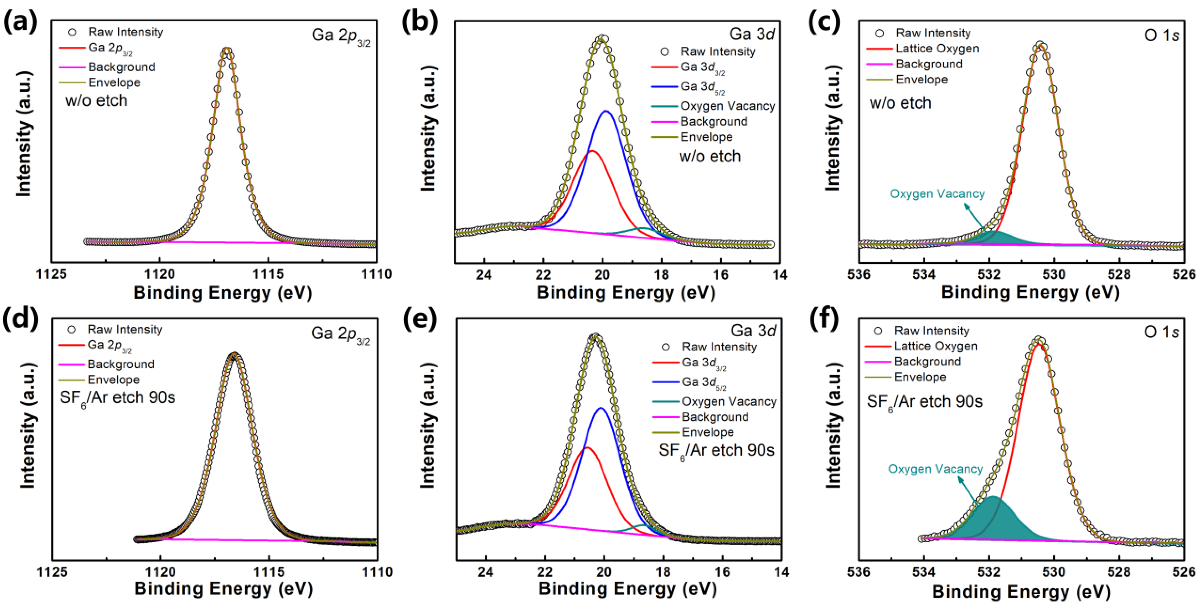
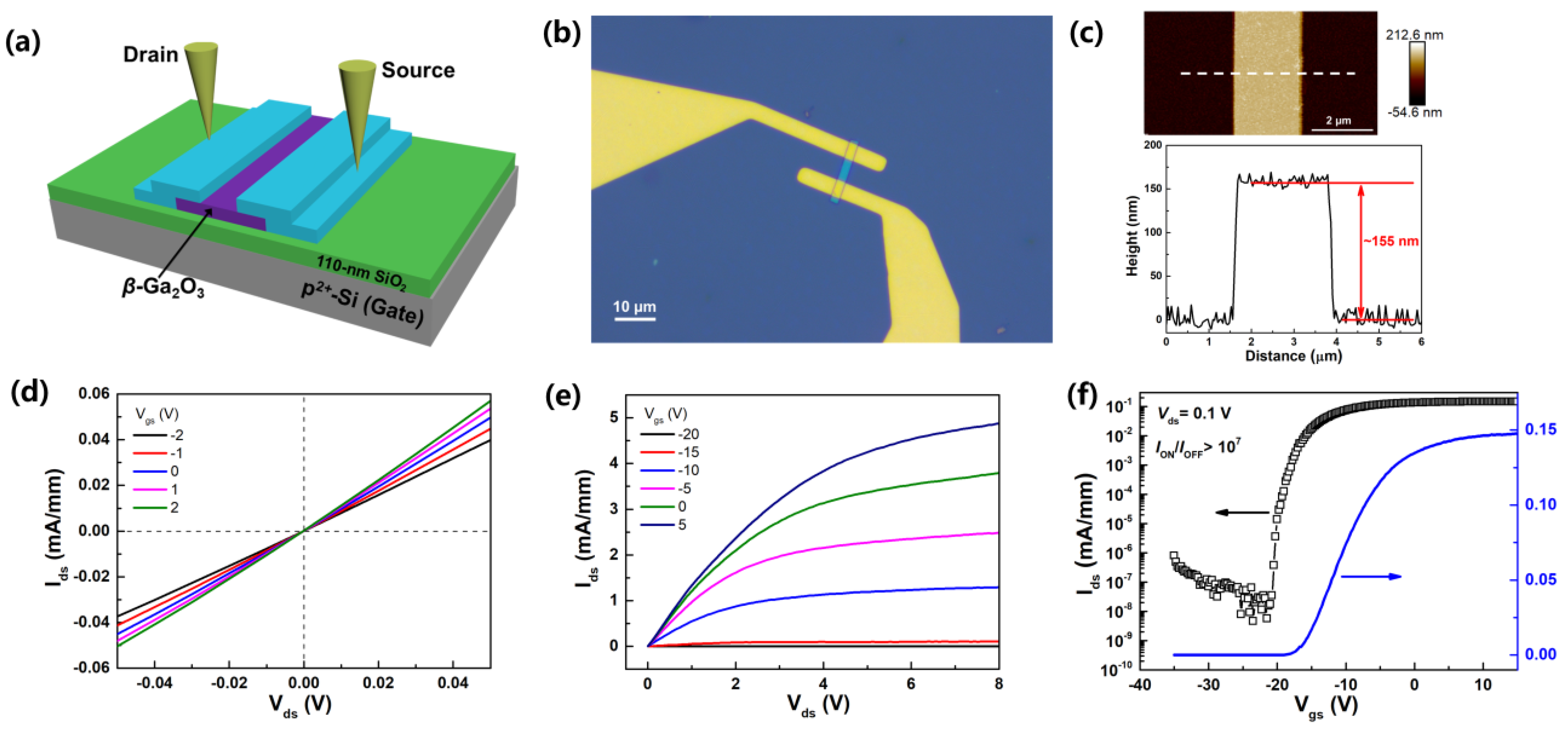
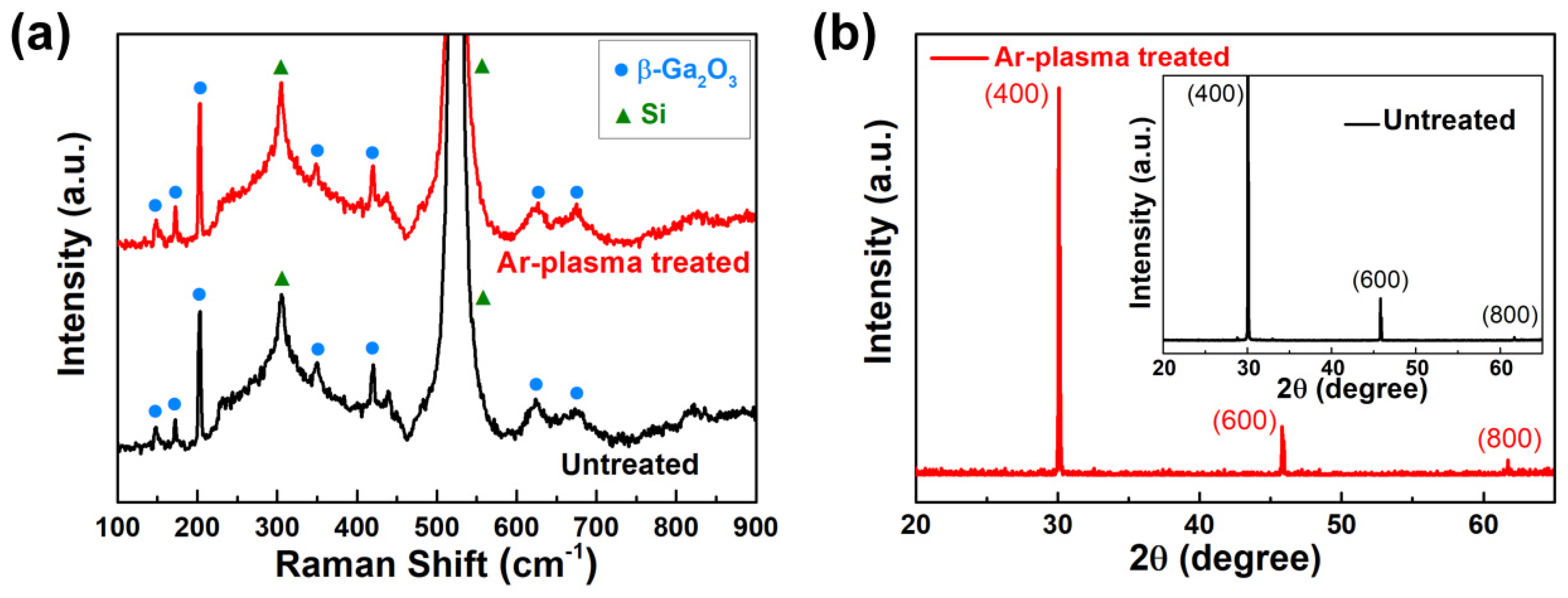
3. Results and Discussion

Prior to the fabrication of transistors, four types of (100)-oriented β-Ga2O3 bulk samples were separately treated with SF6/Ar, SF6/O2/Ar, SF6/O2, and Ar plasmas and comparatively analyzed by XPS. Figure S1a shows the C 1s XPS spectrum of the untreated β-Ga2O3 (100) bulk crystal. The C 1s region arising from surface contamination can be resolved into three subpeaks. The main peak positioned at 284.6 eV can be assigned to alkyl type carbon (C-C), whereas the subpeak (at 286.1 eV) with a binding energy separation of 1.5 eV to the main peak is attributed to the ester (C-O-C) or alcohol (C-OH) functionality. Another subpeak at 288.5 eV is ascribed to the carbon participating at the O-C=O group [7,33,34,35]. Normally, for the untreated bare β-Ga2O3 single crystal, the Ga 2p3/2 plot can be fitted with a single peak ascribed to the Ga-O bond, and the Ga 3d is often deconvoluted into two major components, ascribed to Ga 3d5/2 and Ga 3d3/2 [3,23]. However, in Figure 1b, a very weak subpeak at 18.6 ± 0.2 eV cannot be excluded from the XPS measurements, which is ascribed to the presence of minor oxygen vacancies (VO) in β-Ga2O3 induced by the initial crystal growth process. Figure 1c presents the XPS spectrum of the O 1s core energy level for the untreated β-Ga2O3 bulk sample. Note that the O1s envelope was well fitted by two components. The primary peak positioned at 530.5 ± 0.2 eV corresponds to the lattice oxygen bond (LO), which is closely related to the formation of O2− ions with Ga3+ metal cations [34]. The other subpeak with very weak intensities is located at 531.8 ± 0.2 eV, resulting from the existence of a minor VO at the β-Ga2O3 surface. The VO/(LO + VO) area ratio was extracted to be ~5%, indicating that the content of oxygen vacancy VO in the near-surface region of untreated β-Ga2O3 crystal is very low. It corresponds well with the Ga 3d XPS data above.
After the SF6/Ar plasma treatment, the total peak shape of the C 1s spectrum changed greatly, as shown in Figure S1b. This C 1s signal was still dominated by three species, which are ascribed to adventitious carbon at 284.6 eV, C-O-C or C-OH groups at 286.15 eV, and carboxylate groups at 288.8 eV [33,34,35]. No evident change in the Ga 2p3/2 and Ga 3d core-level peaks was observed, as indicated in Figure 1d,e. Figure 1f shows the O 1s spectrum for the SF6/Ar plasma-treated β-Ga2O3 bulk. Interestingly, the intensity of the oxygen vacancy-related subpeak (at 531.87 ± 0.2 eV) increased obviously as compared with the untreated one. The corresponding VO/(LO + VO) area ratio increased to 18.3%, suggesting a marked rise in oxygen vacancies near the β-Ga2O3 surface, which is beneficial to reducing the contact resistance [23,26]. As previously reported [32], the SF6/Ar plasma treatment process includes the chemical action and physical bombardment. In this progress, SF6 gas can slowly react with the surface of Ga2O3, forming nonvolatile GaFx and volatile SOy based on the reactions Ga2O3 + SF6 → GaFx + SOy. And, the Ar plasma with strong bombardment can eliminate the residual GaFx on the surface. However, the origin of the newly generated oxygen vacancies VO is confusing.
In order to identify the source and create more VO, the SF6/O2/Ar plasma treatment was carried out. The SF6 and O2 gases were, respectively, introduced with the flow rates of 40 and 5 sccm, while the Ar flow rate was set as 30 sccm. The corresponding RIE power was 200 W. The purpose of reactive gas O2 in this procedure is to remove S from SF6 and promote an increase in F concentration based on the reaction SFx + O → F + SOFx-1 (x ≤ 5) [36]. Similarly, there was no noticeable change in the Ga 2p3/2 and Ga 3d core energy levels, as depicted in Figure 2b,c. The addition of O2 was found to barely affect the generation of oxygen vacancies. As can be seen from the O1s signal in Figure 2a, the VO/(LO + VO) area ratio was ~18.8%, slightly higher than the SF6/Ar plasma-treated one. This suggests that enhancing the chemical action of SF6 cannot help to produce more oxygen vacancies VO.
To obtain further insight, we excluded the argon gas from the mixture and performed the SF6/O2 plasma treatment on the β-Ga2O3 crystal. Figure 2d shows the corresponding O1s plot for the SF6/O2-treated β-Ga2O3 bulk sample. Surprisingly, without the assistance of Ar bombardment, the oxygen vacancy-associated subpeak (at 531.95 ± 0.2 eV) was still observable. The ratio of VO/(LO + VO) was up to 17.7%, revealing that appreciable VO exists near the β-Ga2O3 surface. These results are in agreement with the work reported by Jeong et al. [37], suggesting that other ions (e.g., SFx) can also act as a physical bombardment during the plasma process. Moreover, the F 1s signal centered at 685.3 ± 0.2 eV was clearly detected, as displayed in Figure 2e. This peak belongs to the Ga-F bond [2], indicating the formation of non-volatile GaFX at the surface. Jeong et al. [37] proposed that the introduced fluorine atoms may serve as shallow donors in the resistive β-Ga2O3 film and bring about an increase in conductivity. However, the F atoms can behave differently in β-Ga2O3 crystals with different doping concentrations. As can be seen from the two-terminal IV curves in Figure 2f, the n-type β-Ga2O3 nanosheet sample pre-treated with SF6/O2 plasmas exhibited a common Schottky-like behavior, although the conductivity increased compared to the untreated one. Yang et al. [38] recently demonstrated that fluorine plasma treatment can markedly increase the barrier height of β-Ga2O3 Schottky barrier diodes, especially heavily doped or moderately doped β-Ga2O3. This is because the Si donors in β-Ga2O3 materials were compensated by F atoms and formed neutral complexes. Thus, the SF6-based plasma treatments could produce two competing effects. There is a hard tradeoff between ion bombardment-induced vacancies and the F-doping effect. The ion bombardment-caused VO can effectively improve conductivity and reduce the contact resistance [23,30], whereas the F-doping effect can compensate for the n-type dopants in β-Ga2O3 and impair conductivity. In addition, SF6-based gases can evidently etch the gate dielectric layer SiO2 beneath the β-Ga2O3 nanosheet during the device fabrication process, resulting in severe deterioration of the transistor performance. Note that the etch rate of the SiO2 layer by the SF6 plasmas was as high as ~55 nm/min, even faster than that of β-Ga2O3 (i.e., 16 nm/min) [17]. Figure S2 shows photographs of the 110 nm thick SiO2/p-Si substrates with and without SF6 plasma treatment for merely 90 s. Clearly, the SF6-treated SiO2/Si substrate displays the primary color of a silicon wafer, suggesting the absence of a SiO2 layer. Taken together, SF6-contaning plasma is not suitable, while the Ar-plasma treatment seems to be a better choice for achieving Ohmic contact with the heavily doped or moderately doped n-type β-Ga2O3 crystals.
Since XPS can sensitively monitor the evolution of surface chemical states, we performed a systematic XPS analysis on the treated β-Ga2O3 samples with pure Ar-plasmas having different powers and times. Figure S3 shows the corresponding spectra of C 1s among the Ar-treated β-Ga2O3 bulk samples. All of them display the same peak shapes, revealing the existence of the same surface contaminants after Ar-plasma bombardments. Figure 3a–f exhibit the evolution of O 1s core-level spectra of the β-Ga2O3 (100) bulk treated by Ar plasmas with different powers and times. It can be seen that all of the O 1s data were resolved into two kinds of subpeaks. The major peak at 530.5 ± 0.2 eV was identified as lattice oxygen LO (O-Ga bonding state), while another peak at higher binding energies can be credited to the presence of VO. The VO/(LO + VO) ratio continuously evolves with the Ar-plasma power and time. Interestingly, all of the VO/(LO + VO) values surpass the SF6/O2 plasma-treated one, which highlights the advantage of Ar-plasma bombardment in the creation of oxygen vacancies. Figure 4 plots the VO/(LO + VO) area ratio as a function of the treatment time and power. Obviously, the optimal Ar-plasma parameters were 100 W, 60 s. The corresponding VO/(LO + VO) ratio was as high as 45%, suggesting the formation of a great number of VO near the sample surface. Note that the higher power may result in a lower Vo concentration. It is possibly due to the clusters of oxygen vacancy being potentially damaged by a higher power. Yamaga et al. [28] have theoretically proposed that the oxygen vacancy Vo of β-Ga2O3 crystals exists in the form of clusters.
To examine the Ohmic junction formation into β-Ga2O3 devices, the bottom-gated β-Ga2O3 nanosheet transistor was fabricated using the optimized plasma treatment (i.e., Ar-plasma, 100 W, 60 s). Figure 5a presents a schematic of the bottom-gated β-Ga2O3 device structure. The peeled β-Ga2O3 nanosheet served as the conductive channel. Figure 5b shows an optical micrograph of a completed β-Ga2O3 nanosheet transistor on a 110 nm SiO2 bottom-gate oxide. Compared to the traditional 285 nm thick SiO2 layer, the 110 nm thick SiO2 can provide stronger gate modulation in the bottom-gate device configuration. The nanosheet channel length (i.e., Lch) is around 5 μm, and the width of channel (Wch) is ~2.2 μm. Figure 5c shows an AFM micrograph (top) of the corresponding β-Ga2O3 nanosheet channel. The thickness of the nanosheet was measured around 155 nm (bottom). In the absence of post thermal annealing, the fabricated β-Ga2O3 nanosheet FET showed linear Ohmic behavior at a low Vds regime, as displayed in Figure 5d. Figure 5e gives the output characteristics (Ids-Vds) from the β-Ga2O3 nanosheet FET. Well-behaved line shapes were observed, which can be attributed to the presence of effective Ohmic contact. The bottom-gate voltage (Vgs) varies from −20 to 5 V with a step of 5 V. The drain current Ids can be well regulated by the gate bias. Clear pinch-off properties and good current saturation at large Vds values can be seen, indicating good device performance of this n-type nanosheet FET. Figure 5f shows transfer curves (Ids-Vgs) from the β-Ga2O3 nanosheet FET in the log and linear scales at a Vds of 0.1 V. Owing to the formation of effective Ohmic contact, well-behaved electrical characteristics were acquired, including a high ION/IOFF ratio (>107), a small off-state current (IOFF < 0.1 pA), and a small subthreshold slope (SS, 249 mV/dec). These electrical parameters of the fabricated β-Ga2O3 nanosheet device are comparable with those of other reports [9,12]. The field-effect electron mobility ( μ e f f ) was around 21.73 cm2 V−1 s−1, as extracted via
μ e f f = d I d s d V g s L c h W c h C g V d s
where W c h , C g , V d s , and L c h are the channel width, oxide capacitance, drain bias, and channel length of the nanosheet transistor, respectively. V g s and I d s , respectively, denote the bottom-gate bias and drain current in the β-Ga2O3 transistor.
The Y-function method was employed to calculate the contact resistance (RC) of β-Ga2O3 FET via the following equation:
Y = I d s g m = V d s C g W c h μ 0 / L c h · ( V g s V t h )
where g m represents the transconductance. µ0 and V t h are the low-field mobility and threshold voltage, respectively [39,40,41]. The Y-function calculation is capable of extracting the electrical parameters from a transfer curve when drain bias Vds is quite small. The µ0 was calculated to be ~76.07 cm2 V−1 s−1. From the values of V t h and µ0, the RC was extracted as ~104 Ω·mm, which is smaller than the value (i.e., 800 Ω·mm) reported by Jeong et al. [37] for CF4-plasma treated β-Ga2O3. For comparison, Figure S4 shows the IV measurements of the moderately doped β-Ga2O3 nanosheet samples (Ne, ~1018 cm−3) pre-treated with nonoptimal Ar-plasma parameters. All of them exhibit different asymmetric Schottky behaviors. Actually, the contact performance can be further improved by using high-doping-level β-Ga2O3 crystals (Ne, above 1019 cm−3) for plasma treatments. Figure 6a shows the IV curves of the heavily doped β-Ga2O3 (Ne, ~1020 cm−3) channel devices with Ar plasma treatment at various channel sizes (i.e., Lch/S ratio, where S is the cross-sectional area and Lch represents the channel length). Similarly, an excellent linear Ohmic behavior was acquired. The transfer length method (TLM) was employed to determine the contact resistance RC based on the following formula:
Rt = ρ·Lch/S + 2RC
where ρ and Rt are the channel resistivity and total resistance of the heavily doped β-Ga2O3 device, respectively [41]. As displayed in Figure 6b, the RC value obtained from the half of the y-intercept is ~5.2 Ω·mm, which is smaller than that of the moderately doped β-Ga2O3 (Ne, ~1018 cm−3) channel. For comparison, Figure S5 also presents the IV measurements of the heavily doped β-Ga2O3 nanosheet samples (Ne, ~1020 cm−3) pre-treated with nonoptimal Ar-plasma parameters. In this work, hundreds of β-Ga2O3 nanosheet devices were fabricated and analyzed. It was found that the optimized plasma pre-treatment (i.e., Ar plasma, 100 W, 60 s) induces Ohmic contact with great probability, especially for the heavily doped β-Ga2O3 crystals (Ne, ~1020 cm−3). However, the corresponding drain current Ids in this heavily doped channel cannot be effectively turned off by the bottom-gate voltage Vgs, as shown in Figure S6. This is due to the limited gate controllability of the bottom-gated device architecture for the heavily doped β-Ga2O3 channel. High-doping-level channel layers possess high carrier densities, which cannot be fully depleted by the applied bottom-gate bias. Further studies are needed to construct different transistor structures with stronger gate controllability by using this heavily doped β-Ga2O3 channel layer (Ne, ~1020 cm−3) with argon plasma treatments.
To comprehensively analyze the surface defects generated by the Ar plasma treatment (100 W, 60 s), the dual-sweep measurement was performed on the β-Ga2O3 nanosheet FET at a Vds of 1 V, as shown in Figure S7. Evident hysteresis (∆V) can be noticed, suggesting that a large amount of interfacial traps was introduced. The Ar-plasma bombardment has marked side effects on the transistor reverse characteristics. The results are in accordance with the work reported by Yang et al. [39] for the energetic proton irradiation. Moreover, micro–Raman measurements were carried out. Normally, Raman spectroscopy is sensitive to the biaxial strain at the surface region. Figure 7a compares the Raman spectra of the peeled β-Ga2O3 nanosheet on the SiO2/Si (p2+) substrate before and after Ar plasma pre-treatments. Seven phonon peaks near 149, 172, 202, 349, 419, 627, and 674 cm−1 were detected, corresponding to the B g 2 , A g 2 , A g 3 , A g 5 , A g 6 , B g 5 , and A g 9 Raman-active modes. The peaks of the treated β-Ga2O3 nanosheet with Ar plasmas are consistent with that of the untreated one, which reveals that the defects induced by Ar-plasma bombardment did not bring an evident strain-related Raman shift. The Raman results are in agreement with the work reported by Yang et al. and Kwon et al. [17,39]. The potential reason is likely due to the strong particle radiation resistance of β-Ga2O3. Wide-band-gap semiconductors possess an intrinsic radiation hardness [42], particularly β-Ga2O3, due to its greater formation energy of Ga vacancy defect (53.3 eV), compared with 3C-SiC (3.3 eV for Si vacancy) and GaN (7.0 eV for Ga vacancy) [39,43]. The fluctuation of both base lines in the micro-Raman spectra is mostly due to the impact of the SiO2/Si (p2+) substrate beneath the transferred β-Ga2O3 nanosheet. In addition, the micro–X-ray diffraction (micro–XRD) patterns of the β-Ga2O3 nanosheet before and after the Ar plasma treatments were also measured to evaluate the stress state of the material, as shown in Figure 7b. In the inset, the pattern exhibits three diffraction peaks located at 30.07°, 45.79°, and 61.69°, which is in good agreement with the monoclinic structure from the standard card (PDF#43-1012). The peaks can be respectively assigned to the (400), (600), and (800) crystal planes. After Ar plasma pre-treatment, the positions of the diffraction peaks nearly remained constant (i.e., 30.07°, 45.81°, and 61.73°), which reveals that the lattice strain induced by Ar-plasma bombardment was negligible.

4. Conclusions

In summary, four types of plasma treatments (i.e., gas mixtures SF6/Ar, SF6/O2/Ar, SF6/O2, and Ar) were conducted to investigate their impacts on generating oxygen vacancies. High-resolution XPS was employed to examine the evolution of the surface chemical states of (100)-oriented β-Ga2O3 crystals. The optimal treatment process parameters (i.e., argon, 100 W, 60 s) were extracted, which can generate appreciable oxygen vacancies at the (100) β-Ga2O3 surface. With the optimized Ar plasma pre-treatment, the resultant (100) β-Ga2O3 nanosheet FET exhibits effective Ohmic contacts (i.e., RC = 104 Ω·mm) without any post-metallization anneal, resulting in well-behaved electrical performance, such as a high ION/IOFF ratio (> 107), a steep subthreshold slope SS (249 mV/dec), and acceptable μ e f f (~21.73 cm2 V−1 s−1). Lower contact resistance RC (i.e., 5.2 Ω·mm) can be obtained by using heavily doped β-Ga2O3 crystals (Ne, ~1020 cm−3) for the Ar plasma treatments. These results highlight its potential to improve the contact properties of Ga2O3-based electronic devices by using a facile, environmental, and controllable argon plasma treatment technique.

Supplementary Materials

The following supporting information can be downloaded at https://www.mdpi.com/article/10.3390/electronics13163181/s1, Figure S1: C1s XPS spectra after charge correction from the β-Ga2O3 (100) bulk samples treated with various mixture gases: (a) untreated, (b) SF6/Ar plasmas, (c) SF6/O2/Ar plasmas, and (d) SF6/O2 plasmas. Figure S2: Photograph of the 110 nm thick SiO2/p2+-Si substrates with (left) and without (right) SF6 plasma treatment for merely 90s. Figure S3: C1s XPS spectra after charge correction from the bulk β-Ga2O3 (100) crystals treated by argon plasmas with different powers and time: (a) 100 W, 30 s; (b) 100 W, 60 s; (c) 100 W, 90 s; (d) 200 W, 30 s; (e) 200 W, 60 s; and (f) 200 W, 90 s. Figure S4: IV measurements of the moderately doped β-Ga2O3 nanosheet samples (Ne, ~1018 cm−3) pretreated by Ar plasmas with different powers and time: (a) untreated; (b) 100 W, 30 s; (c) 100 W, 90 s; (d) 200 W, 30 s; (e) 200 W, 60 s; and (f) 200 W, 90 s. Figure S5: IV measurements of the heavily doped β-Ga2O3 nanosheet samples (Ne, ~1020 cm−3) pre-treated by Ar plasmas with different powers and time: (a) untreated; (b) 100 W, 30 s; (c) 100 W, 90 s; (d) 200 W, 30 s; (e) 200 W, 60 s; and (f) 200 W, 90 s. Figure S6: Transfer characteristics from the heavily doped β-Ga2O3 nanosheet bottom-gate devices with different Lch/S ratios. Figure S7: Hysteretic transfer characteristics of a β-Ga2O3 nanosheet FET pre-treated with Ar plasmas.

Author Contributions

Conceptualization J.-X.C.; Methodology, J.-X.C.; Software, J.-X.C. and B.-Y.L.; Formal analysis, J.-X.C. and Y.G.; Investigation, J.-X.C. and B.-Y.L.; Data curation, J.-X.C.; Writing—original draft, J.-X.C.; Writing—review and editing, B.L.; Visualization, Y.G.; Supervision, B.-Y.L. and B.L.; Funding acquisition, B.L. All authors have read and agreed to the published version of the manuscript.

Funding

This research is supported by the National Natural Science Foundation of China (Nos. 62104072 and 62174058) and the Postdoctoral Research Program of Guangzhou (No. L2230350).

Data Availability Statement

The data are contained within the article and Supplementary Materials.

Conflicts of Interest

The authors declare no conflicts of interests.

References

  1. Pearton, S.J.; Yang, J.; Cary IV, P.H.; Ren, F.; Kim, J.; Tadjer, M.J.; Mastro, M.A. A Review of Ga2O3 Materials, Processing, and Devices. Appl. Phys. Rev. 2018, 5, 011301. [Google Scholar] [CrossRef]
  2. Feng, L.; Li, Y.; Su, X.; Wang, S.; Liu, H.; Wang, J.; Gong, Z.; Ding, W.; Zhang, Y.; Yun, F. Growth and Characterization of Spindle-Like Ga2O3 Nanocrystals by Electrochemical Reaction in Hydrofluoric Solution. Appl. Surf. Sci. 2016, 389, 205–210. [Google Scholar] [CrossRef]
  3. Chen, J.X.; Ta, J.J.; Ma, H.P.; Zhang, H.; Feng, J.J.; Liu, W.J.; Xia, C.; Lu, H.L.; Zhang, D.W. Band Alignment of AlN/β-Ga2O3 Heterojunction Interface Measured by X-ray Photoelectron Spectroscopy. Appl. Phys. Lett. 2018, 112, 261602. [Google Scholar] [CrossRef]
  4. Lee, Y.; Johnson, N.R.; George, S.M. Thermal Atomic Layer Etching of Gallium Oxide Using Sequential Exposures of HF and Various Metal Precursors. Chem. Mater. 2020, 32, 5937–5948. [Google Scholar] [CrossRef]
  5. Lv, Y.; Zhou, X.; Long, S.; Song, X.; Wang, Y.; Liang, S.; He, Z.; Han, T.; Tan, X.; Feng, Z.; et al. Source-Field-Plated β-Ga2O3 MOSFET with Record Power Figure of Merit of 50.4 MW/cm2. IEEE Electron Device Lett. 2019, 40, 83. [Google Scholar] [CrossRef]
  6. Liu, Z.; Wang, X.; Liu, Y.; Guo, D.; Li, S.; Yan, Z.; Tan, C.K.; Li, W.; Li, P.; Tang, W. A High-Performance Ultraviolet Solar-Blind Photodetector Based on a β-Ga2O3 Schottky Photodiode. J. Mater. Chem. C 2019, 7, 13920–13929. [Google Scholar] [CrossRef]
  7. O’Donoghue, R.; Rechmann, J.; Aghaee, M.; Rogalla, D.; Becker, H.W.; Creatore, M.; Wieck, A.D.; Devi, A. Low Temperature Growth of Gallium Oxide Thin Films via Plasma Enhanced Atomic Layer Deposition. Dalton Trans. 2017, 46, 16551–16561. [Google Scholar] [CrossRef] [PubMed]
  8. Chen, J.X.; Li, X.X.; Ta, J.J.; Cui, H.Y.; Huang, W.; Ji, Z.G.; Sai, Q.L.; Xia, C.T.; Lu, H.L.; Zhang, D.W. Fabrication of a Nb-Doped β-Ga2O3 Nanobelt Field-Effect Transistor and Its Low-Temperature Behavior. ACS Appl. Mater. Interfaces 2020, 12, 8437–8445. [Google Scholar] [CrossRef] [PubMed]
  9. Kim, J.; Oh, S.; Mastro, M.A.; Kim, J. Exfoliated β-Ga2O3 Nano-Belt Field-Effect Transistors for Air-Stable High Power and High Temperature Electronics. Phys. Chem. Chem. Phys. 2016, 18, 15760. [Google Scholar] [CrossRef] [PubMed]
  10. Baliga, B.J. Power Semiconductor Device Figure of Merit for High-Frequency Applications. IEEE Electron Device Lett. 1989, 10, 455–457. [Google Scholar] [CrossRef]
  11. Chen, J.X.; Liu, B.Y.; Gu, Y.; Chen, R.; Li, B.; Zhou, C. Influence of Ultralow Temperature on Quasi-2-D β-Ga2O3 Field-Effect Transistors. IEEE Trans. Electron Devices 2024, 71, 4233–4239. [Google Scholar] [CrossRef]
  12. Kim, J.; Mastro, M.A.; Tadjer, M.J.; Kim, J. Quasi-Two-Dimensional h-BN/β-Ga2O3 Heterostructure Metal-Insulator-Semiconductor Field-Effect Transistor. ACS Appl. Mater. Interfaces 2017, 9, 21322–21327. [Google Scholar] [CrossRef] [PubMed]
  13. Galazka, Z.; Irmscher, K.; Uecker, R.; Bertram, R.; Pietsch, M.; Kwasniewski, A.; Naumann, M.; Schulz, T.; Schewski, R.; Klimm, D.; et al. On the Bulk β-Ga2O3 Single Crystals Grown by the Czochralski Method. J. Cryst. Growth 2014, 404, 184–191. [Google Scholar] [CrossRef]
  14. Aida, H.; Nishiguchi, K.; Takeda, H.; Aota, N.; Sunakawa, K.; Yaguchi, Y. Growth of β-Ga2O3 Single Crystals by the Edge-Defined, Film Fed Growth Method. Jpn. J. Appl. Phys. 2008, 47, 8506–8509. [Google Scholar] [CrossRef]
  15. Hoshikawa, K.; Ohba, E.; Kobayashi, T.; Yanagisawa, J.; Miyagawa, C.; Nakamura, Y. Growth of β-Ga2O3 Single Crystals Using Vertical Bridgman Method in Ambient Air. J. Cryst. Growth 2016, 447, 36. [Google Scholar] [CrossRef]
  16. Vo, T.H.; Kim, S.; Kim, H.Y.; Park, J.H.; Jeon, D.W.; Hwang, W.S. Temperature-Dependent Capacitance-Voltage Characteristics of β-Ga2O3 Schottky Barrier Diodes with (001) Epitaxial Grown Layer Using MOCVD. Mater. Sci. Semicond. Process. 2024, 173, 108130. [Google Scholar] [CrossRef]
  17. Kwon, Y.; Lee, G.; Oh, S.; Kim, J.; Pearton, S.J.; Ren, F. Tuning the Thickness of Exfoliated Quasi-Two-Dimensional β-Ga2O3 Flakes by Plasma Etching. Appl. Phys. Lett. 2017, 110, 131901. [Google Scholar] [CrossRef]
  18. Liu, Y.; Wang, P.; Wang, Y.; Lin, Z.; Liu, H.; Huang, J.; Huang, Y.; Duan, X. Van der Waals Integrated Devices Based on Nanomembranes of 3D Materials. Nano Lett. 2020, 20, 1410–1416. [Google Scholar] [CrossRef] [PubMed]
  19. Zhou, H.; Si, M.; Alghamdi, S.; Qiu, G.; Yang, L.; Ye, P.D. High-Performance Depletion/Enhancement Mode β-Ga2O3 on Insulator (GOOI) Field-Effect Transistors with Record Drain Currents of 600/450 mA/mm. IEEE Electron Device Lett. 2017, 38, 103–106. [Google Scholar] [CrossRef]
  20. Ma, J.; Cho, H.J.; Heo, J.; Kim, S.; Yoo, G. Asymmetric Double-Gate β-Ga2O3 Nanomembrane Field-Effect Transistor for Energy-Efficient Power Devices. Adv. Electron. Mater. 2019, 5, 1800938. [Google Scholar] [CrossRef]
  21. Tan, P.; Zou, Y.; Zhao, X.; Hou, X.; Zhang, Z.; Ding, M.; Yu, S.; Ma, X.; Xu, G.; Hu, Q.; et al. Hysteresis-Free Ga2O3 Solar-Blind Phototransistor Modulated from Photoconduction to Photogating Effect. Appl. Phys. Lett. 2022, 120, 071106. [Google Scholar] [CrossRef]
  22. Chen, J.X.; Li, X.X.; Huang, W.; Ji, Z.G.; Wu, S.Z.; Xiao, Z.Q.; Ou, X.; Zhang, D.W.; Lu, H.L. High-Energy X-ray Radiation Effects on the Exfoliated Quasi-Two-Dimensional β-Ga2O3 Nanoflake Field-Effect Transistors. Nanotechnology 2020, 31, 345206. [Google Scholar] [CrossRef] [PubMed]
  23. Li, Z.; Liu, Y.; Zhang, A.; Liu, Q.; Shen, C.; Wu, F.; Xu, C.; Chen, M.; Fu, H.; Zhou, C. Quasi-Two-Dimensional β-Ga2O3 Field Effect Transistors with Large Drain Current Density and Low Contact Resistance via Controlled Formation of Interfacial Oxygen Vacancies. Nano Res. 2019, 12, 143–148. [Google Scholar] [CrossRef]
  24. Yao, Y.; Davis, R.F.; Porter, L.M. Investigation of Different Metals as Ohmic Contacts to β-Ga2O3: Comparison and Analysis of Electrical Behavior, Morphology, and Other Physical Properties. J. Electron. Mater. 2017, 46, 2053–2060. [Google Scholar] [CrossRef]
  25. Chen, J.X.; Li, X.X.; Ma, H.P.; Huang, W.; Ji, Z.G.; Xia, C.; Lu, H.L.; Zhang, D.W. Investigation of the Mechanism for Ohmic Contact Formation in Ti/Al/Ni/Au Contacts to β-Ga2O3 Nanobelt Field-Effect Transistors. ACS Appl. Mater. Interfaces 2019, 11, 32127–32134. [Google Scholar] [CrossRef] [PubMed]
  26. Guo, D.Y.; Wu, Z.P.; An, Y.H.; Guo, X.C.; Chu, X.L.; Sun, C.L.; Li, L.H.; Li, P.G.; Tang, W.H. Oxygen Vacancy Tuned Ohmic-Schottky Conversion for Enhanced Performance in β-Ga2O3 Solar-Blind Ultraviolet Photodetectors. Appl. Phys. Lett. 2014, 105, 023507. [Google Scholar] [CrossRef]
  27. Liu, T.; Feng, Z.; Li, Q.; Yang, J.; Li, C.; Dupuis, M. Role of Oxygen Vacancies on Oxygen Evolution Reaction Activity: β-Ga2O3 as a Case Study. Chem. Mater. 2014, 30, 7714–7726. [Google Scholar] [CrossRef]
  28. Yamaga, M.; Víllora, E.G.; Shimamura, K.; Ichinose, N.; Honda, M. Donor Structure and Electric Transport Mechanism in β-Ga2O3. Phys. Rev. B 2003, 68, 155207. [Google Scholar] [CrossRef]
  29. Hajnal, Z.; Miró, J.; Kiss, G.; Réti, F.; Deák, P.; Herndon, R.C.; Kuperberg, J.M. Role of Oxygen Vacancy Defect States in the n-Type Conduction of β-Ga2O3. J. Appl. Phys. 1999, 86, 3792–3796. [Google Scholar] [CrossRef]
  30. Narayanan, M.; Shah, A.P.; Ghosh, S.; Thamizhavel, A.; Bhattacharya, A. Elucidating the Role of Oxygen Vacancies on the Electrical Conductivity of β-Ga2O3 Single-Crystals. Appl. Phys. Lett. 2023, 123, 172106. [Google Scholar] [CrossRef]
  31. Higashiwaki, M.; Sasaki, K.; Kuramata, A.; Masui, T.; Yamakoshi, S. Gallium Oxide (Ga2O3) Metal-Semiconductor Field-Effect Transistors on Single-Crystal β-Ga2O3 (010) Substrates. Appl. Phys. Lett. 2012, 100, 013504. [Google Scholar] [CrossRef]
  32. Liang, H.; Chen, Y.; Xia, X.; Zhang, C.; Shen, R.; Liu, Y.; Luo, Y.; Du, G. A Preliminary Study of SF6 Based Inductively Coupled Plasma Etching Techniques for Beta Gallium Trioxide Thin Film. Mater. Sci. Semicond. Process. 2015, 39, 582–586. [Google Scholar] [CrossRef]
  33. Bourque, J.L.; Biesinger, M.C.; Baines, K.M. Chemical State Determination of Molecular Gallium Compounds Using XPS. Dalton Trans. 2016, 45, 7678–7696. [Google Scholar] [CrossRef] [PubMed]
  34. Tao, J.; Lu, H.L.; Gu, Y.; Ma, H.P.; Li, X.; Chen, J.X.; Liu, W.J.; Zhang, H.; Feng, J.J. Investigation of Growth Characteristics, Compositions, and Properties of Atomic Layer Deposited Amorphous Zn-Doped Ga2O3 Films. Appl. Surf. Sci. 2019, 476, 733–740. [Google Scholar] [CrossRef]
  35. Ilhom, S.; Mohammad, A.; Shukla, D.; Grasso, J.; Willis, B.G.; Okyay, A.K.; Biyikli, N. Low-Temperature As-Grown Crystalline β-Ga2O3 Films via Plasma-Enhanced Atomic Layer Deposition. ACS Appl. Mater. Interfaces 2021, 13, 8538–8551. [Google Scholar] [CrossRef]
  36. Tezani, L.L.; Pessoa, R.S.; Maciel, H.S.; Petraconi, G. Chemistry Studies of SF6/CF4, SF6/O2, and CF4/O2 Gas Phase during Hollow Cathode Reactive Ion Etching Plasma. Vacuum 2014, 106, 64–68. [Google Scholar] [CrossRef]
  37. Jeong, Y.J.; Yang, J.Y.; Lee, C.H.; Park, R.; Lee, G.; Chung, R.B.K.; Yoo, G. Fluorine-Based Plasma Treatment for Hetero-Epitaxial β-Ga2O3 MOSFETs. Appl. Surf. Sci. 2021, 558, 149936. [Google Scholar] [CrossRef]
  38. Yang, J.; Fares, C.; Ren, F.; Sharma, R.; Patrick, E.; Law, M.E.; Pearton, S.J.; Kuramata, A. Effects of Fluorine Incorporation into β-Ga2O3. J. Appl. Phys. 2018, 123, 165706. [Google Scholar] [CrossRef]
  39. Yang, G.; Jang, S.; Ren, F.; Pearton, S.J.; Kim, J. Influence of High-Energy Proton Irradiation on β-Ga2O3 Nanobelt Field-Effect Transistors. ACS Appl. Mater. Interfaces 2017, 9, 40471–40476. [Google Scholar] [CrossRef] [PubMed]
  40. Chang, H.Y.; Zhu, W.; Akinwande, D. On the Mobility and Contact Resistance Evaluation for Transistors Based on MoS2 or Two-Dimensional Semiconducting Atomic Crystals. Appl. Phys. Lett. 2014, 104, 113504. [Google Scholar] [CrossRef]
  41. Cao, Q.; Han, S.J.; Tulevski, G.S.; Franklin, A.D.; Haensch, W. Evaluation of Field-Effect Mobility and Contact Resistance of Transistors that Use Solution-Processed Single-Walled Carbon Nanotubes. ACS Nano 2012, 6, 6471–6477. [Google Scholar] [CrossRef] [PubMed]
  42. Kim, J.; Pearton, S.J.; Fares, C.; Yang, J.; Ren, F.; Kim, S.; Polyakov, A.Y. Radiation Damage Effects in Ga2O3 Materials and Devices. J. Mater. Chem. C 2019, 7, 10–24. [Google Scholar] [CrossRef]
  43. Sfuncia, G.; Nicotra, G.; Giannazzo, F.; Pécz, B.; Gueorguiev, G.K.; Georgieva, A.K. 2D Graphitic-Like Gallium Nitride and Other Structural Selectivity in Confinement at the Graphene/SiC Interface. CrystEngComm 2023, 25, 5810–5817. [Google Scholar] [CrossRef]
Figure 1. XPS results for the (100)-oriented β-Ga2O3 bulk samples. (a) Ga 2p3/2, (b) Ga 3d, and (c) O 1s core-level spectra from the pristine β-Ga2O3 without any plasma treatments. (d) Ga 2p3/2, (e) Ga 3d, and (f) O 1s core-level spectra from the β-Ga2O3 treated with SF6/Ar plasmas.
Electronics 13 03181 g001
Figure 2. XPS results for (100) β-Ga2O3 bulk samples. (a) O 1s, (b) Ga 2p3/2, and (c) Ga 3d core-level spectra from the β-Ga2O3 treated with SF6/O2/Ar plasmas. (d) O 1s and (e) F 1s core-level spectra from the β-Ga2O3 treated with SF6/O2 plasmas. (f) Two-terminal IV curves of the β-Ga2O3 nanosheet pre-treated with (red) and without (black) SF6/O2 plasmas.
Electronics 13 03181 g002
Figure 3. XPS spectra of O 1s for the (100) β-Ga2O3 bulk samples treated by Ar plasmas with different power and time: (a) 100 W, 30 s; (b) 100 W, 60 s; (c) 100 W, 90 s; (d) 200 W, 30 s; (e) 200 W, 60 s; and (f) 200 W, 90 s.
Electronics 13 03181 g003
Figure 4. The VO/(LO + VO) area ratio for the Ar-treated β-Ga2O3 (100) bulk samples as a function of treatment time and power.
Electronics 13 03181 g004
Figure 5. (a) Schematic view of the bottom-gated β-Ga2O3 nanosheet transistor with a 110 nm thick SiO2 gate insulator. (b) Optical microscopy image of a prepared β-Ga2O3 nanosheet-based FET. (c) Thickness profile and optical micrograph from the peeled β-Ga2O3 nanosheet as acquired by AFM. (d) IV characteristics at a low Vds regime for this β-Ga2O3 nanosheet FET. (e) Output curves (Ids-Vds) from the β-Ga2O3 nanosheet FET. (f) Transfer characteristics (Ids-Vbg) obtained from the β-Ga2O3 nanosheet transistor.
Electronics 13 03181 g005
Figure 6. Contact resistance in the heavily doped β-Ga2O3 nanosheet samples (Ne, ~1020 cm−3). (a) IV curves of the heavily doped β-Ga2O3 devices with different Lch/S ratios determined by TLM. (b) Total resistance (Rt) plotted as a function of the Lch/S ratio in β-Ga2O3 devices.
Electronics 13 03181 g006
Figure 7. (a) Micro-Raman spectra for the peeled β-Ga2O3 nanosheet on the SiO2/Si (p2+) substrate before and after Ar plasma pre-treatment (100 W, 60 s). (b) Micro-XRD pattern for the peeled β-Ga2O3 nanosheet on the SiO2/Si (p2+) substrate after Ar plasma pre-treatment. The inset gives the micro-XRD pattern of the β-Ga2O3 nanosheet before Ar plasma pre-treatment.
Electronics 13 03181 g007
Disclaimer/Publisher’s Note: The statements, opinions and data contained in all publications are solely those of the individual author(s) and contributor(s) and not of MDPI and/or the editor(s). MDPI and/or the editor(s) disclaim responsibility for any injury to people or property resulting from any ideas, methods, instructions or products referred to in the content.

