Article

State Space Average Modeling, Small Signal Analysis, and Control Implementation of an Efficient Single-Switch High-Gain Multicell Boost DC-DC Converter with Low Voltage Stress

1
Electrical Engineering Department, Faculty of Engineering-Rabigh, King Abdulaziz University, Jeddah 21589, Saudi Arabia
2
Electrical Engineering Department, Faculty of Engineering, Menoufia University, Shebin El-Kom 32511, Egypt
3
Department of Electrical Engineering, College of Engineering, Northern Border University, Arar 1321, Saudi Arabia
4
Department of Electrical Engineering and Computer Science, Khalifa University, Abu Dhabi 127788, United Arab Emirates
5
Department of Electromechanical, Systems and Metal Engineering, Ghent University, 9000 Ghent, Belgium
6
Electrical Engineering Department, Faculty of Engineering, Beni-Suef University, Beni-Suef 62511, Egypt
*
Authors to whom correspondence should be addressed.
Electronics 2024, 13(16), 3264; https://doi.org/10.3390/electronics13163264 (registering DOI)
Submission received: 11 July 2024 / Revised: 12 August 2024 / Accepted: 12 August 2024 / Published: 17 August 2024
(This article belongs to the Special Issue Advanced Technologies in Power Electronics and Electric Drives)

Abstract

:
This paper presents the closed-loop control of a single-switch high-gain multicell boost DC-DC converter working in a continuous conduction mode (CCM). This converter is particularly designed for applications in photovoltaic systems. One of the main advantages of the proposed converter is that it only employs one active semiconductor switch, which decreases the converter losses and cost, increases the efficiency, and simplifies the control circuit. Moreover, the multicell nature of the proposed converter offers the possibility of obtaining the required voltage gain by selecting the number of cells. State space average (SSA) modeling and small-signal analysis are used to model the switching converter power stages of the proposed converter. The parasitic series resistances of the passive elements of the converter circuit are considered to improve the accuracy of the modeling. Small-signal analysis is used to derive the open-loop transfer functions, input-to-output and control-to-output transfer functions of the proposed converter to examine its dynamic performance. The stability of the converter is analyzed to design the parameters of the voltage controller using the proposed modeling method. The experimental prototype of the proposed single-switch two-cell boost DC-DC converter was implemented. The simulation and experimental results proved the effectiveness of the proposed boost DC-DC converter under different working conditions. It has a fast dynamic response without overshoots. A comprehensive comparison between the proposed converter and previous boost converters is provided. It guarantees a required variable and constant high voltage gain with a wider duty ratio range. It compromises between the required performance, the low number of components, low voltage stress on the components, and cost-effectiveness. The experimental efficiency of the proposed converter is about 96% at a 100 W load.

1. Introduction

The global need for electricity is increasing all the time. Because of the poor supply and high cost of traditional energy sources, there is a growing need to use renewable energy sources (RESs). Among these renewable energy sources, photovoltaics (PVs), wind turbines (WTs), and fuel cells (FCs) have developed rapidly in recent decades. To tie these sources with the utility grid, the low DC output voltage levels produced by them must be boosted to high DC voltage levels. High-voltage gain DC-DC converters are widely utilized in a diversity of applications, such as RESs, uninterruptible power supplies (UPSs), new-energy electric vehicles (NEEVs), aircraft power supply systems, railway energy storage systems, etc. [1,2,3]. High-boosting DC-DC converters are often employed to increase voltage and efficiency in diverse ways, each with its own set of advantages and disadvantages [4].
Non-isolated standard DC-DC converters are characterized by their simple installation, ease of control circuit use, and low cost. But despite these features, they are not suitable for applications that require high voltage gain due to the need to work at large duty cycle values. This, in turn, leads to more switching and conduction losses at constant input voltage, increasing input current ripples and decreasing system effectiveness [5].
Several innovative DC-DC topologies have been developed to accomplish significant extreme voltage gain. Isolated and non-isolated are the types of high-gain DC-DC topologies. Isolated topologies have significant issues, such as heat effects, voltage ripples on the power switches, core saturation, and leakage inductance, and their enormous volume makes them more costly. Non-isolated types are used instead for their better voltage gain; they are more compact and less expensive because no galvanic isolation is required [6,7,8,9,10,11,12,13,14,15,16,17,18,19,20,21,22,23,24,25]. A non-isolated step-up interleaved converter was introduced in [6]. High voltage gain with a minimal switch voltage stress was satisfied, but it has more components and is not suitable for applications that require smaller gain or lighter loads. In [7], a conventional DC-DC boost converter was linked to a switched capacitor and coupled inductor to raise the voltage gain and efficacy. Nevertheless, inductor core losses continue to be affected by excessive input current ripples. To obtain high voltage gain with a moderate duty cycle and increase efficiency, the interleaved boost converter was introduced in [8,9]. However, they have difficulty separating gate signals, raising costs. Furthermore, the voltage gain was like that of a traditional boost converter. Reference [10] proposed a variety of switched capacitor-based DC-DC boost converters, while [11] employed a switched capacitor/inductor. Although high voltage gain was achieved, they had significant conduction losses, severe switching stresses, and complicated circuits. A cascaded boost converter that provides high voltage gain with minimal switching losses and current ripples was employed in [12]. However, drawbacks, such as increased costs, decreased efficiency, and the complexity of the control system, were identified. A single-cell DC-DC topology based on a hybrid switched inductor was introduced in [13]. High voltage gain, low power switching stresses, and high efficiency were satisfied. However, the number of components in this converter diminished efficiency while increasing the circuit’s cost and size. Reference [14] proposed a single-switch DC-DC-boosting topology based on a traditional boost converter, voltage lift method, and a switched capacitor. Also, a single-switch DC-DC converter based on a traditional boost converter and a switched capacitor was suggested in [15]. High efficiency and small voltage stresses through the main switch and diodes were attained, but the voltage gain was still small compared with other topologies, and the number of converter components was large. A non-isolated DC-DC boost converter achieved by merging a dual step-up converter with a switching inductor topology was provided in [16]. High voltage gain, low switching losses, and small voltage stresses across the switches were accomplished, but the large number of components increased the size of the converter. In [17], a DC-DC converter with a voltage multiplier cell (VMC) was described. High voltage gain, minimal voltage stress across the switches, and great efficiency were noted. On the other hand, the large component count increased the topology dimensions and costs. A single-switch DC-DC topology was introduced in [18]. The design of this converter featured a double voltage lift approach, and it comprised a VMC, a super lift Luo converter, and a cascaded step-up topology. Issues relating to high-voltage gain and minimum input current ripples were addressed, but the large number of components reduced the converter efficiency. Reference [19] offered a new SEPIC boost DC-DC topology. The semiconductor switches operated with soft switching, which reduced the converter losses and enhanced the efficiency. Nevertheless, the voltage gain was not very high, and the number of components was large. Other topologies such as quasi-Z-source, quasi-Y-source, or a combination between them were found in [20,21,22,23]. Even though these topologies provide substantial voltage gain with low duty cycles and constant input current, they have restricted duty cycles, severe stresses on the main switch, and complicated driving circuits. Reference [24] developed a DC-DC converter that employed VMC with a voltage extend circuit to increase the voltage gain. It was possible to achieve extreme voltage gain and minimal voltage stresses on the active components. However, the input current was discontinuous since the primary switch was connected directly with the input DC source, and the number of components was large. In addition, as the number of cells increased, converter efficiency fell. The topologies found in [25,26,27,28,29,30] introduced variety of designs based on quad-switched inductors, a combination of boost and SEPIC, switched inductors, or active-passive inductor cells. Although the voltage gain derived from these converters was greater than that from the conventional, some of them had a large number of components [25,27,29,30], and others had a large number of switches [26,28,29], which, in turn, made the control circuit problematic, increased the losses, and raised costs. To address the aforementioned issues, a modified DC-DC step-up converter was developed and presented in [31]. Its characteristics included continuous input current, easy control, extreme voltage gain, and low voltage stress on the active switches. Likewise, cascading extra cells with ultra-high voltage gain can be provided. To model, analyze, and design such converters, developed tools such as state space average (SSA) modeling and small signal analysis were introduced [32,33,34,35,36]. Solving the state space equations of such DC-DC converters is more challenging because the duty cycle serves as the converters’ control input. The behavior of the DC-DC converters is nonlinear and time-varying. However, in order to design the controller, the system must be linear and time-invariant. Therefore, the state space average model (SSAM) and the small signal model (SSM) are used for this purpose. In [32], the SSAM of a boost DC-DC converter considering all the parasitic elements was presented. The transfer functions of a proposed AC-AC converter were derived in [33] using the SSM and the gains of proportional-integral (PI) voltage controller based on the stability analysis using the frequency response method. In [34], small signal analysis and PI controller implementation of a boost converter-fed permanent magnet DC (PMDC) motor for electric vehicle (EV) applications were introduced. In [35], the various principles of SSAM of DC-DC boost converters operating in CCM were presented. The effects of parasitic elements were also included. In [36], a two-loop control strategy for a current-fed half-bridge (CFHB) DC-DC converter was presented. Both the current control loop and the voltage control loop are designed at a phase margin of 60°. The stability of the control system was validated using PSIM software. In [37,38], electrothermal average models of a diode–IGBT switch and a diode-MOSFET switch for modeling the DC-DC converters were introduced, respectively. The equations used in the introduced models allow modeling the converter operation in both CCM and discontinuous conduction mode (DCM). In [39], an average SSM of a conventional boost DC-DC converter in CCM considering the switching power loss was presented. In [40], a reduced average model of a high-voltage gain DC-DC converter with multicell diode-capacitor network considering ideal components was presented to overcome the complexity of the multicell converter modeling. The reduced model was used to simplify the closed-loop controller design.
In this paper, an SSAM and an SSM of a novel single switch high gain multicell boost DC-DC converter are developed considering the series parasitic resistances of the passive elements. With the help of the developed models, an extensive analysis is conducted to investigate the steady state and dynamic characteristics of the proposed converter. A small signal model and the corresponding control-to-output and input-to-output open-loop transfer functions of the proposed topology are presented. The stability analysis of the proposed topology is presented to design the voltage controller of the proposed converter. The validity of the developed SSAM of the proposed converter is emphasized through experimental verification of the proposed single switch two-cell boost DC-DC converter. Different results are presented under different operating conditions.
The advantages of the single switch two-cell boost DC-DC converter are as follows:
  • Low voltage stress on the main switch and diodes.
  • Simplicity of control due to single-switch topology.
  • The structure of the converter can be extended to n cells for high voltage gain.
  • Compact size and minimum number of components guarantee a cost-effective converter.
  • Good robustness of the closed-loop control under different working conditions.

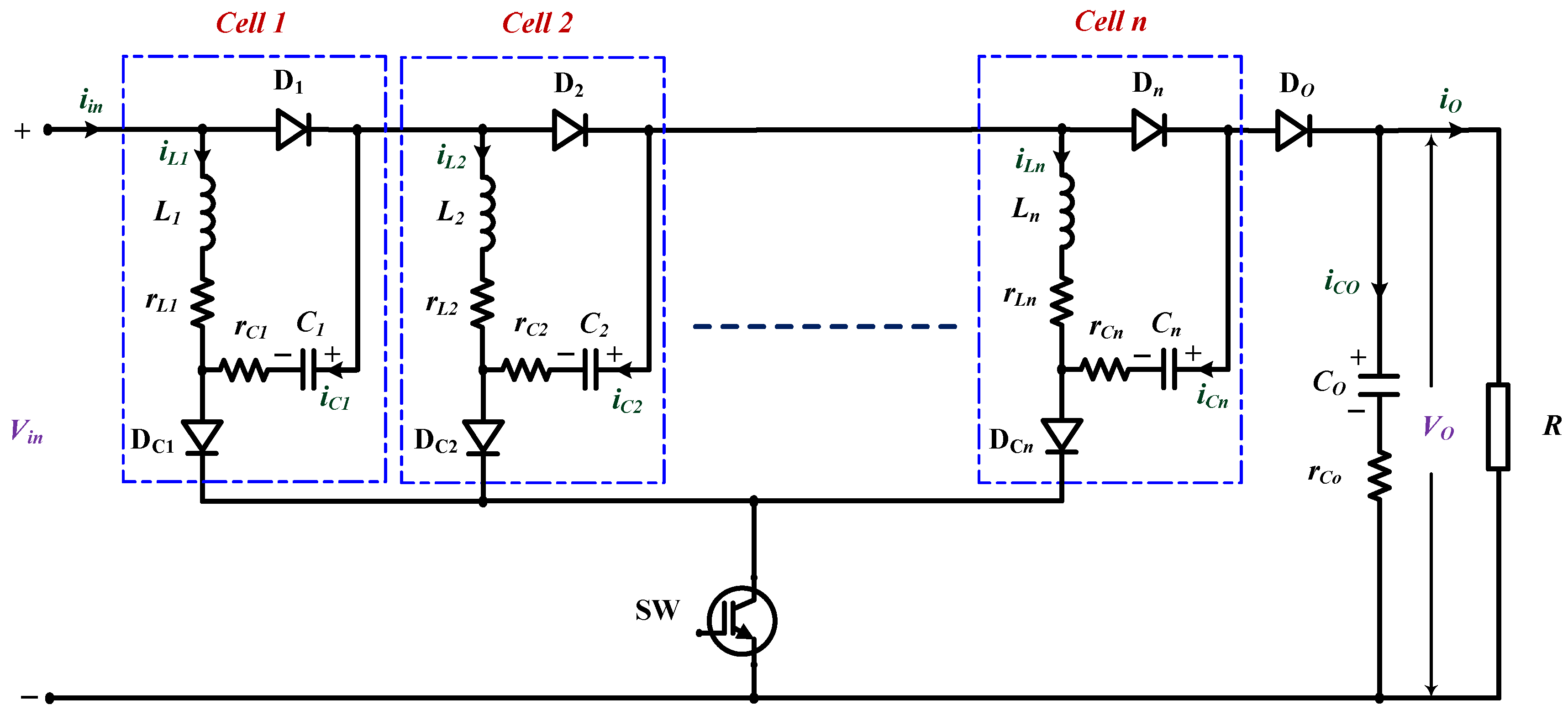
2. Proposed Converter Topology

Figure 1 displays a new topology for a single-switch multicell step-up DC-DC converter [31]. The proposed converter topology consists of only one semiconductor switch (SW) that controls the power flow from the input side (supply) to the output side (load) through switching on and off, n cells, output diode, and an output capacitor. Each cell of the proposed converter circuit consists of one inductor, one capacitor, and two diodes. In [31], the circuit description and its modes of operation were explained in detail. The steady-state behavior of the proposed converter was analyzed. Also, the voltage gain in continuous conduction mode (CCM) was evaluated. According to this, the voltage gain of n cells is given by the following formula:
g = 2 d 1 d + 2 ( n 1 )
where g is the voltage gain and d is the main switch duty ratio.

3. State Space Average Modeling

The following assumptions are considered when deriving the SSAM of the proposed topology:
  • The semiconductor switch is on (i.e., closed) for a time dTs and is off (i.e., open) for a time (1d)Ts during a switching period time Ts.
  • The duty ratio (d) is expressed as the ratio of the time the switch is on (on time) over the switching period time Ts. The switching frequency (Fs) is given as Fs = 1/Ts.
  • The converter works in the CCM, considering the design considerations of inductors and capacitors as follows:
    L n = d n + 1 d i   g 2 R T s C n = g 2 T s v R 1 d n + 1 d C o = 1 d T s v R g n + 1 d 1
    where Ln is the inductance of cell n, Cn is the capacitance of cell n, Co is the output capacitance, R is the load resistance, ∆i is the allowable percentage of the inductor current ripple, and ∆v is the allowable percentage of the capacitor voltage ripple.
  • The semiconductor switch and all diodes are modeled as ideal semiconductor devices.
  • The parasitic series resistances of the passive elements (i.e., inductors and capacitors) are taken into consideration.

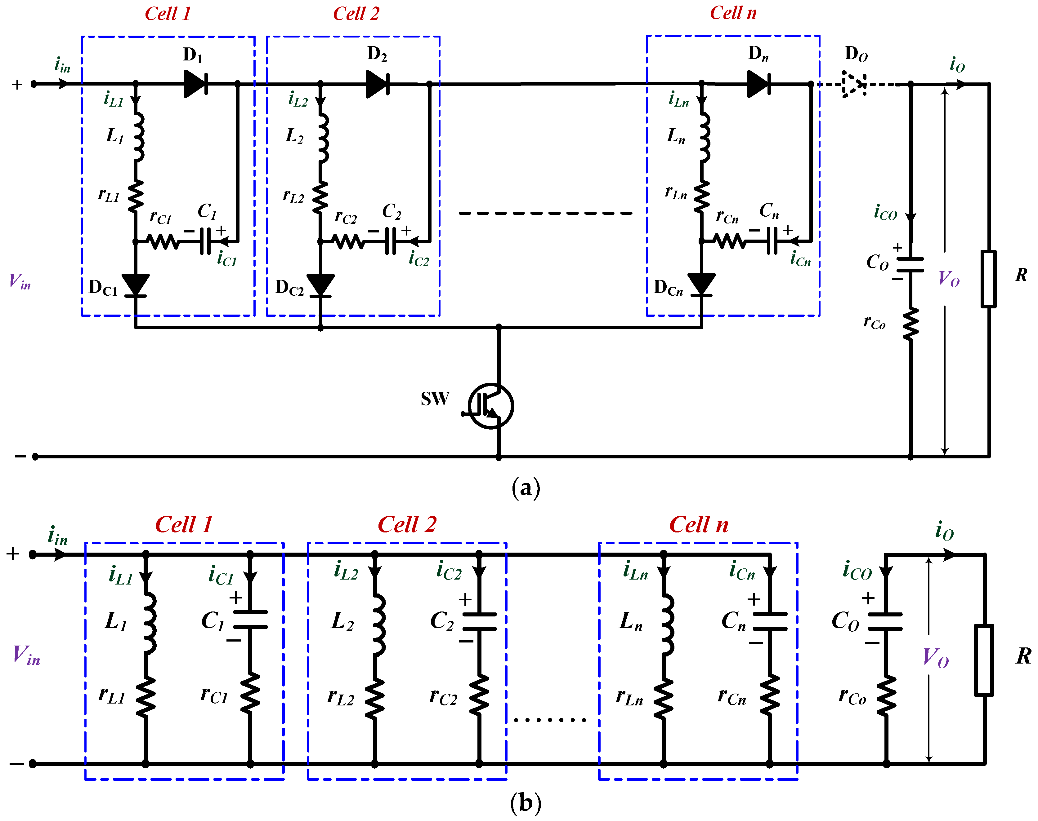
3.1. On State (0 < t < dTs)

Figure 2 illustrates the on-state equivalent circuit of the proposed multicell converter. The active and inactive semiconductor devices are shown in Figure 2a, while the analogous circuit diagram of the converter is displayed in Figure 2b. In the on state, the semiconductor switch and all diodes except the output diode (Do) are closed.
Using Kirchhoff’s voltage law (KVL), the differential equations of each converter cell are derived as
v i n = i L i   r L i + L i d i L i d t
v i n = i C i   r C i + v C i = r C i   C i d v C i d t + v C i
where vin refers to the input voltage, and Li and rLi are the inductance and the equivalent series resistances (ESR) of the inductor of cell i, respectively. Ci and rCi are the capacitance and the ESR of the capacitor of cell i, respectively, while iLi and vCi are the inductor current and the capacitor voltage of the cell i, respectively.
Using KVL/KCL (Kirchhoff’s current law), the differential equations of the output circuit are derived as
i o = i C o
where io and iCo are the output current and the current via the output capacitor, respectively. These currents are given as
i o = v o R = i C o r C o + v C o   R
i C o = C o d v C o d t
where Co and rCo are capacitance and ESR of the output capacitor, respectively. vo and vCo are the output voltage and the output capacitor voltage, respectively, and R is the output (load) resistance.
For SSAM, the inductor current for the converter cell iLi, the capacitor voltage for the converter cell vCi, and the voltage across the output capacitor vCo are considered as state variables. Therefore, for an n cell converter, there are 2n + 1 state variables. Using Equations (3)–(7), the differentiation of the state variables is given as
d i L i d t = 1 L i V i n r L i L i i L i
d v C i d t = 1 r C i   C i V i n 1 r C i   C i v C i
d v C o d t = 1 C o   ( r C o + R ) v C o
Since the state space equations in the on state can be given as
x ˙ = A 1 x + B 1 u
y = C 1 x + E 1 u
Therefore:
d i L 1 d t d v C 1 d t d i L 2 d t d v C 2 d t d i L n d t d v C n d t d v C o d t = r L 1 L 1 0 0 0 0 0 0 0 0 1 r C 1 C 1 0 0 0 0 0 0 0 0 r L 2 L 2 0 0 0 0 0 0 0 0 1 r C 2 C 2 0 0 0 0 0 0 0 0 0 0 0 0 0 0 0 0 r L n L n 0 0 0 0 0 0 0 0 1 r C n C n 0 0 0 0 0 0 0 0 1 C o r C o + R   i L 1 v C 1 i L 2 v C 2 i L n v C n v C o + 1 L 1 1 r C 1 C 1 1 L 2 1 r C 2 C 2 1 L n 1 r C n C n 0 v i n
The output voltage in the on state is given as
v o = 0 0 0 0 0 0 R r C o + R i L 1 v C 1 i L 2 v C 2 i L n v C n v C o + 0 v i n

3.2. Off State (dTs < t < Ts)

Figure 3 illustrates the off-state equivalent circuit of the proposed multicell converter. The active and inactive semiconductor devices are shown in Figure 3a, while the analogous circuit diagram is illustrated in Figure 3b. In the off state, the semiconductor switch and all diodes except the output diode (Do) are open. Using KVL/KCL, the general differential equation of the multicell converter in the off state is derived as
v i n = i = 1 n i L i   r L i + L i d i L i d t i C i   r C i v C i + v o
Since
i C i = i L i
Therefore,
v i n = i = 1 n i L i r L i + r C i + L i d i L i d t v C i + v o
Since
i L 1 = i L 2 = i L n
Therefore,
i o = i L 1 i C o
Using Equations (17)–(19), the differentiation of the state variables is given as
d i L i d t = 1 n L i v i n + α i i L i + 1 L i v C i 1 n L i R r C o + R v C o
where
α i = 1 L i r L i + r C i + r C o   R n   r C o + R
d v C i d t = 1 C i i L i
d v C o d t = R C o   ( r C o + R ) i L 1 + 1 C o   ( r C o + R ) v C o
where iL1 is the inductor current of cell 1. Since the state space equations in the off state can be given as
x ˙ = A 2 x + B 2 u
y = C 2 x + E 2 u
Therefore:
d i L 1 d t d v C 1 d t d i L 2 d t d v C 2 d t d i L n d t d v C n d t d v C o d t = α 1 1 L 1 0 0 0 0 0 1 n L 1 R r C o + R 1 C 1 0 0 0 0 0 0 0 0 0 α 2 1 L 2 0 0 0 1 n L 2 R r C o + R 0 0 1 C 2 0 0 0 0 0 0 0 0 0 0 0 0 0 0 0 0 0 α n 1 L n 1 n L n R r C o + R 0 0 0 0 0 1 C n 0 0 R C o r C o + R 0 0 0 0 0 0 1 C o r C o + R   i L 1 v C 1 i L 2 v C 2 i L n v C n v C o + 1 n L 1 0 1 n L 2 0 1 n L n 0 0 v i n
where α1, α2 and αn are
α 1 = 1 L 1 r L 1 + r C 1 + r C o R n r C o + R
α 2 = 1 L 2 r L 2 + r C 2 + r C o R n r C o + R
α n = 1 L n r L n + r C n + r C o R n r C o + R
The output voltage in the off state is given as
v o = r C o R r C o + R 0 0 0 0 0 R r C o + R i L 1 v C 1 i L 2 v C 2 i L n v C n v C o + 0 v i n

3.3. Average Model

Since the SSAM expresses the average behavior of the state variables over a switching period, the state space averaged description is given as
x ˙ = A x + B u
y = C x + E u
where the A, B, C, and E matrices are given as
A = d A 1 + d A 2
B = d B 1 + d B 2
C = d C 1 + d C 2
E = d E 2 + d E 2
where
d = 1 d
Hence
A = r L 1 L 1 d + α 1 d 1 L 1 d 0 0 0 0 0 1 n L 1 R r C o + R d 1 C 1 d 1 r C 1 C 1 d 0 0 0 0 0 0 0 0 r L 2 L 2 d + α 2 d 1 L 2 d 0 0 0 1 n L 2 R r C o + R d 0 0 1 C 2 d 1 r C 2 C 2 d 0 0 0 0 0 0 0 0 0 0 0 0 0 0 0 0 r L n L n d + α n d 1 L n d 1 n L n R r C o + R d 0 0 0 0 0 1 C n d 1 r C n C n d 0 R C o r C o + R d 0 0 0 0 0 0 1 C o r C o + R
B = d L 1 + d n L 1 d r C 1 C 1 d L 2 + d n L 2 d r C 2 C 2 d L n + d n L n d r C n C n 0
C = r C o R d r C o + R 0 0 0 0 0 R r C o + R
E = 0
At steady state,
x ˙ = 0
Therefore, the average values of the state variables of the proposed multicell step-up converter are calculated as
x = A 1 B u

4. Small Signal Analysis

Small signal analysis is a useful technique for examining the dynamic performance and stability of power electronics converters. It can be used to determine the transfer functions to examine the output performance of the power electronics converters against disturbances or variations in the input. To obtain the SSM of the proposed single-switch multicell step-up DC-DC converter, a perturbation in all variables of the SSAM is introduced around the steady-state operating point such that
x = X + x ~
u = U + u ~
y = Y + y ~
d = D + d ~
d = D d ~
D = 1 D
v i n = V i n + v ~ i n
v o = V o + v ~ o
where the capitalized quantities (X, Y, D, Vin, …) are the steady state values (DC values) and the dashed quantities ( x ~ , y ~ , d ~ , v ~ i n , …) are small perturbations (AC values). Since the SSAM can be given as
d x d t = ( d A 1 + d A 2 ) x + ( d B 1 + d B 2 ) u
Therefore,
d ( X + x ~ ) d t = ( ( D + d ~ ) A 1 + ( D d ~ ) A 2 ) X + x ~ + ( ( D + d ~ ) B 1 + ( D d ~ ) B 2 ) ( U + u ~ )
Hence,
d x ~ d t = ( D A 1 + D A 2 ) X + ( D B 1 + D B 2 ) U + ( D A 1 + D A 2 ) x ~ + ( D B 1 + D B 2 ) u ~ + A 1 A 2 X + B 1 B 2 U d ~ + A 1 A 2 + B 1 B 2 d ~ x ~
The previous equation consists of five terms. The first term is neglected because it is DC (steady state). The fifth term is a second-order term. It is also neglected because the value obtained from multiplication of the two incremental terms (around the equilibrium point) would be very small compared to the first-order terms, while the other three terms are first-order linear terms. Therefore, the state space equations of SSM can be given as
d x ~ d t = ( D A 1 + D A 2 ) x ~ + ( D B 1 + D B 2 ) u ~ + A 1 A 2 X + B 1 B 2 U d ~
Using the same previous procedure:
y ~ = ( D C 1 + D C 2 ) x ~ + ( D E 1 + D E 2 ) u ~ + C 1 C 2 X + E 1 E 2 U d ~
Therefore, the duty cycle to the output voltage (control-to-output) transfer function Gvd(s) of the proposed multicell converter can be given as
G v d s = v ~ o s d ~ s v ~ i n s = 0 = ( D C 1 + D C 2 ) ( s I ( D A 1 + D A 2 ) ) 1 ( A 1 A 2 X + B 1 B 2 U ) + C 1 C 2 X + E 1 E 2 U
where I is the identity matrix, while the input voltage to the output voltage (input-to-output) transfer function Gvg(s) of the proposed multicell converter can be given as
G v g s = v ~ o s v ~ i n ( s ) d ~ s = 0 = ( D C 1 + D C 2 ) ( s I ( D A 1 + D A 2 ) ) 1 ( D B 1 + D B 2 ) + ( D E 1 + D E 2 )
Table 1 displays the parameters of the proposed single-switch two-cell boost DC-DC converter that are used for the simulation and experimental purposes.
Using Equation (57), the open-loop control-to-output transfer function Gvd(s) of the proposed two-cell boost converter is determined as
G v d s = 0.2113   s 5 7.348 × 10 4 s 4 7.793 × 10 9 s 3 2.379 × 10 14 s 2 + 2.022 × 10 18 s + 9.906 × 10 20 s 5 + 1.783 × 10 5 s 4 + 8.049 × 10 9 s 3 + 8.928 × 10 12 s 2 + 1.529 × 10 16 s + 5.981 × 10 18
Using Equation (58), the open-loop input-to-output transfer function Gvg(s) of the proposed two-cell boost converter is determined as
G v g s = 26.45   s 4 + 1.095 × 10 7 s 3 + 1.46 × 10 12 s 2 + 6.207 × 10 16 s + 2.854 × 10 19 s 5 + 1.783 × 10 5 s 4 + 8.049 × 10 9 s 3 + 8.928 × 10 12 s 2 + 1.529 × 10 16 s + 5.981 × 10 18

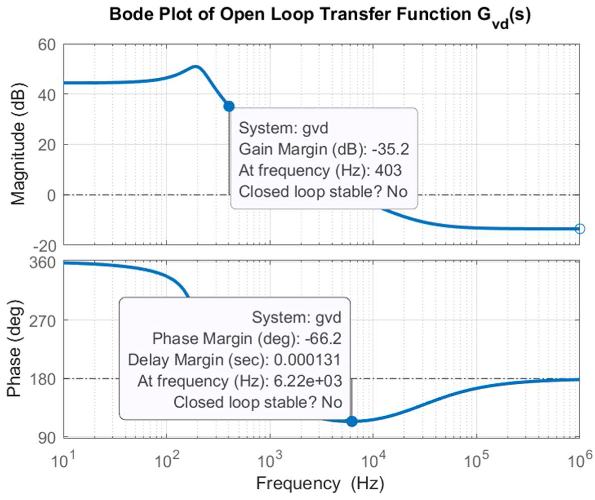
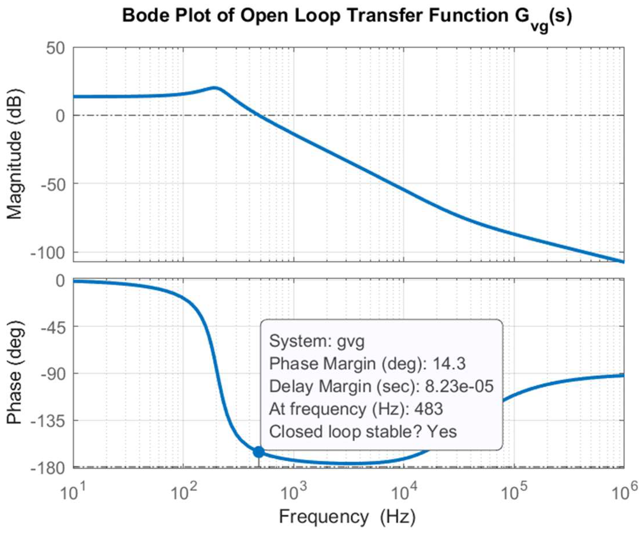
5. Stability Analysis

As important measures of the converter stability, Figure 4 illustrates the bode plot diagram of the open-loop control-to-output transfer function Gvd(s) of the suggested two-cell boost converter, while the root locus diagram is shown in Figure 5. It is found that the gain margin Gm = −35.2 dB at phase crossover frequency Fcp = 403 Hz and phase margin Pm = −66.2° at gain crossover frequency Fcg = 6220 Hz, which refers to the instability. Also, as shown in Figure 5, there is a zero on the right half side of the s-plane.
Figure 6 illustrates the bode plot diagram of the open-loop input-to-output transfer function Gvg(s) of the proposed two-cell boost converter, while the root locus diagram is displayed in Figure 7. It is found that the phase margin Pm = 14.3° at gain crossover frequency Fcg = 483 Hz, which refers to the stability.

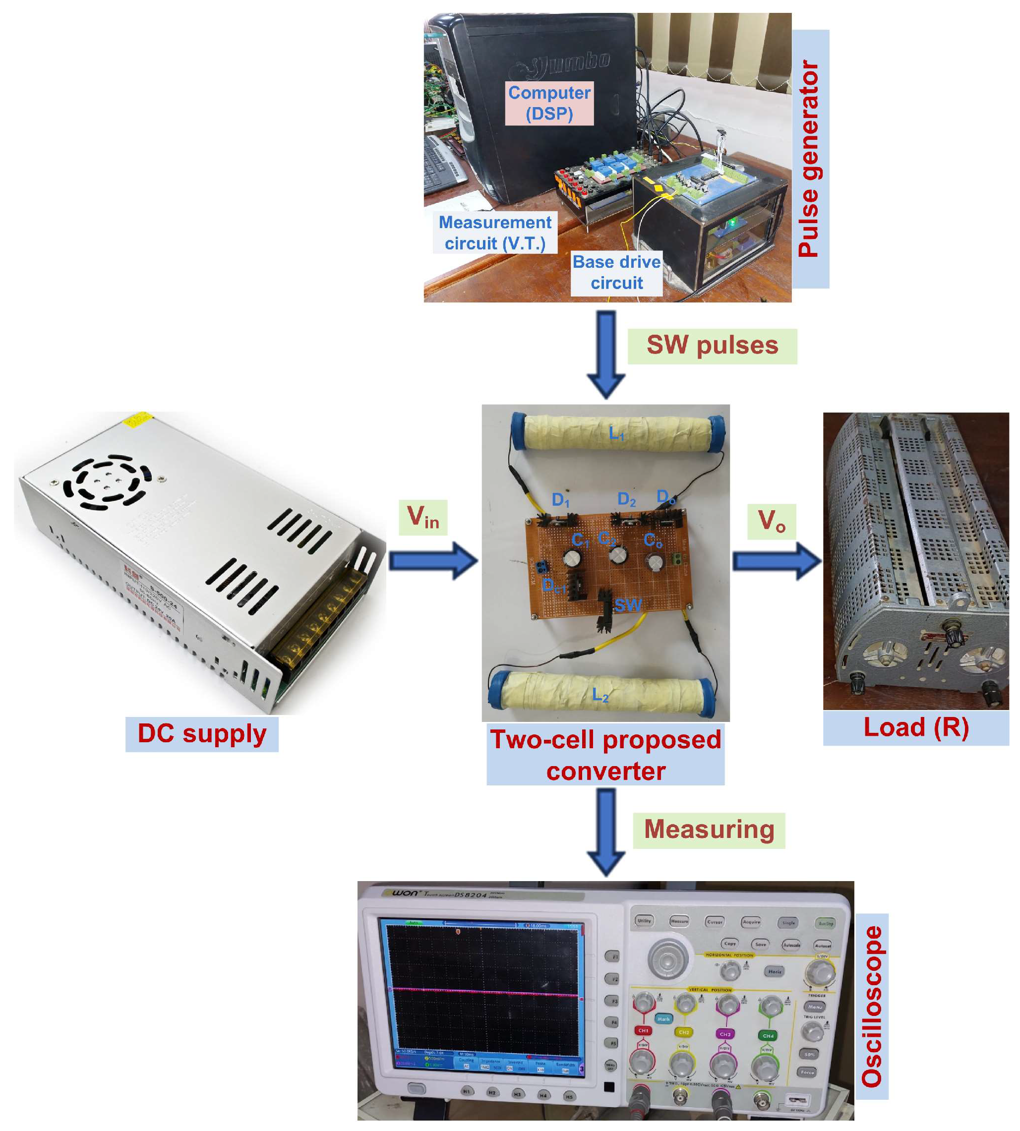
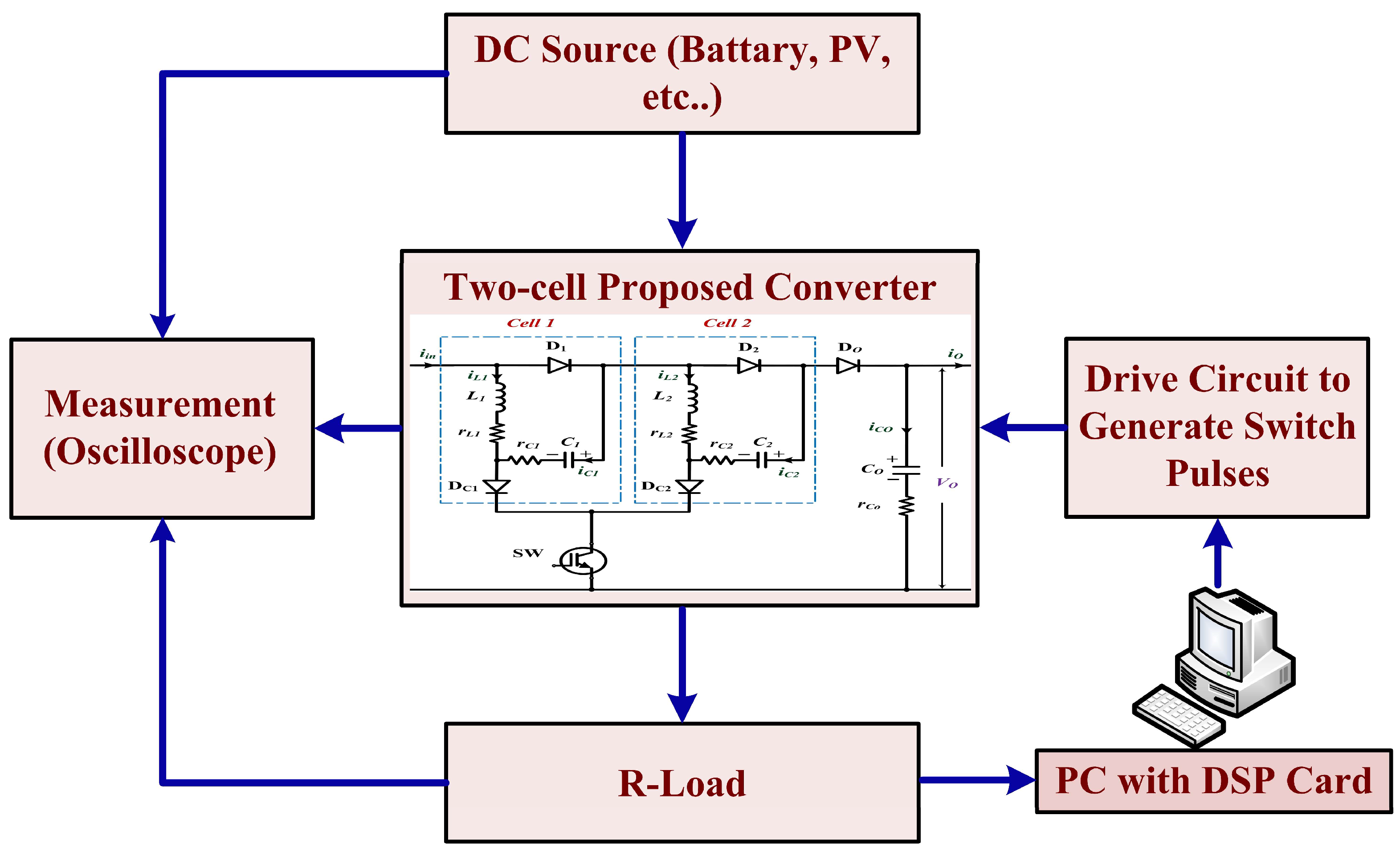
6. Experimental System Setup

To prove the validity of the developed SSAM of the proposed multicell converter, an experimental setup of the presented topology with two cells (n = 2) has been built and its performance has been compared with the simulated performance based on the SSAM of the suggested converter.
Figure 8 shows a photo of the actual experimental setup of the proposed single-switch two-cell boost DC-DC converter. It consists of a DC power supply (24 V, 20 A), a single-switch two-cell proposed boost DC-DC converter, a resistive load, a function generator (AFG-3051, 50 MHz, GW Instek, Taipei, Taiwan), a digital storage oscilloscope (TDS8204, 200 MHz, 2 GSa/s, Owon, Zhangzhou, China), a digital signal processor (DS1104, dSPACE, Paderborn, Germany), a voltage transducer (LV 25-p, LEM, Meyrin, Switzerland), and a drive circuit. The proposed converter is supplied from a DC source 24 V to supply a resistive load of 130 Ω by controlling the power switch pulses that come from the function generator with a switching frequency of 5 KHz. The oscilloscope is used to capture the voltage and current waveforms. The proposed converter circuit is examined in both open-loop and closed-loop operations. The schematic diagram for the experimental setup system is shown in Figure 9. This system shows the system structure for open-loop and closed-loop operations.

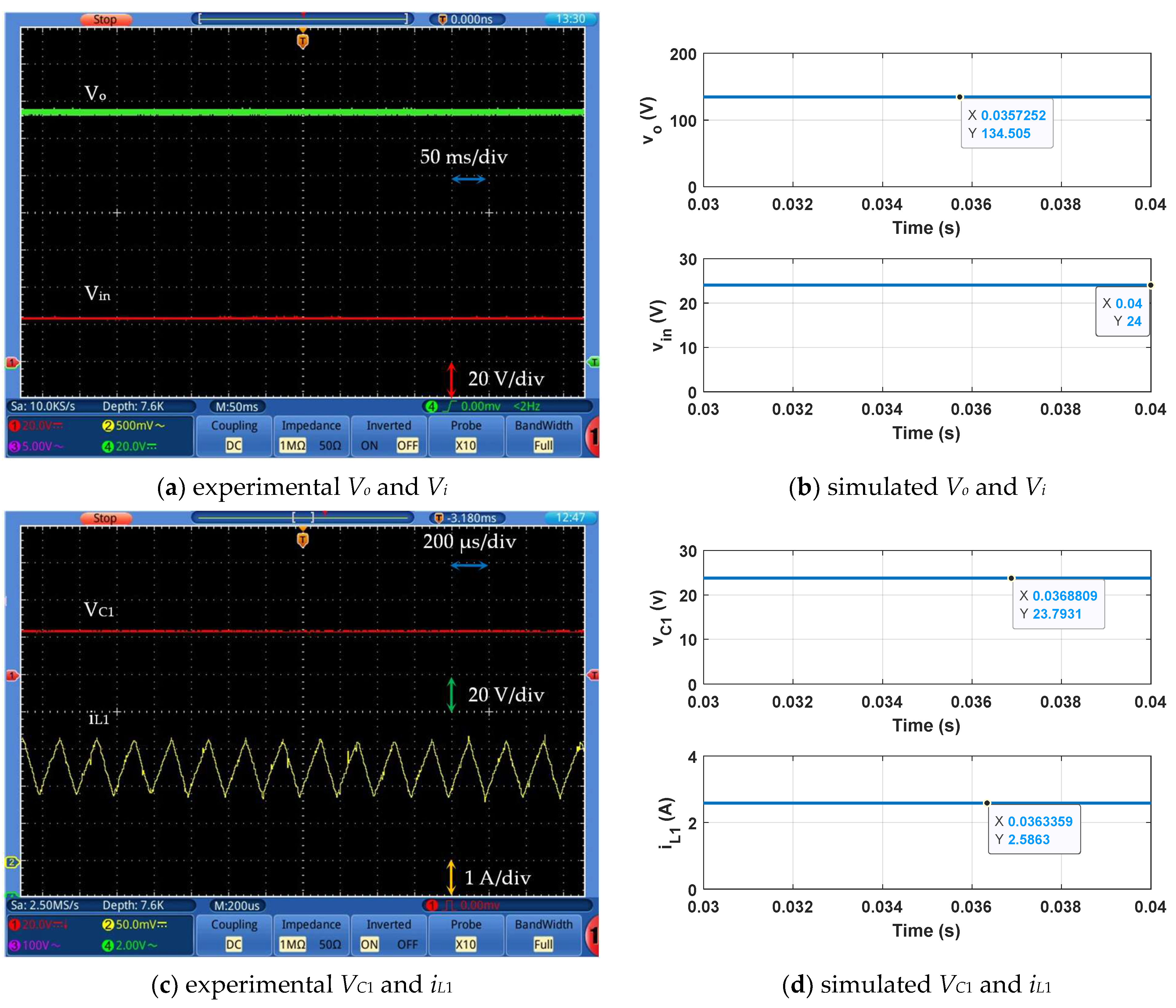
7. Open-Loop Performance

The proposed single-switch two-cell boost DC-DC converter is first examined in the open-loop operation. Figure 10 and Figure 11 show the comparison between the experimental and simulated SSAM open-loop performance of the proposed single-switch two-cell boost DC-DC converter at duty cycles D = 0.5 and D = 0.6, respectively. The simulation results are obtained using Matlab R2023b software. The steady-state average values of the variables (Vo, VC1, iL1, VC2, and iL2) of the SSAM of the suggested topology are compared to the corresponding experimental switching waveforms captured from the actual laboratory setup at steady state at the same input voltage Vin = 24 V. As shown in Figure 10, the SSAM simulation gives a theoretical average output voltage (Vo) of 114.54 V, while the output voltage of the experimental converter oscillates between 113 V and 117 V due to switching (experimental average of (113 + 117)/2 = 115 V). Therefore, the theoretical average (114.54 V) and the experimental average (115 V) of the output voltage are very close, which proves the SSAM validation. Also, the inductor currents (iL1 and iL2) are similar in experimental and simulation tests. The steady-state value of the simulated inductor current-based SSAM of the converter has a value of 1.76 A, while the steady-state experimental inductor current (iL1 or iL2) oscillates between 1.1 A and 2.6 A (experimental average of (1.1 + 2.6)/2 = 1.85 A). Moreover, the capacitors’ voltages (vC1 and vC2) are similar in experimental and simulation tests.
The steady-state simulated capacitor voltage has a value of 23.79 V, while the corresponding steady-state experimental capacitor voltage (vC1 or vC2) oscillates between 23.5 V and 24 V. Similar performances are obtained when the converter is operated at duty cycle D = 0.6, as shown in Figure 11. The SSAM smooths out the switching ripple inherent in the state variables of the experimental converter. Moreover, the comparison between the obtained simulation and experimental results validates the developed SSAM of the proposed converter.

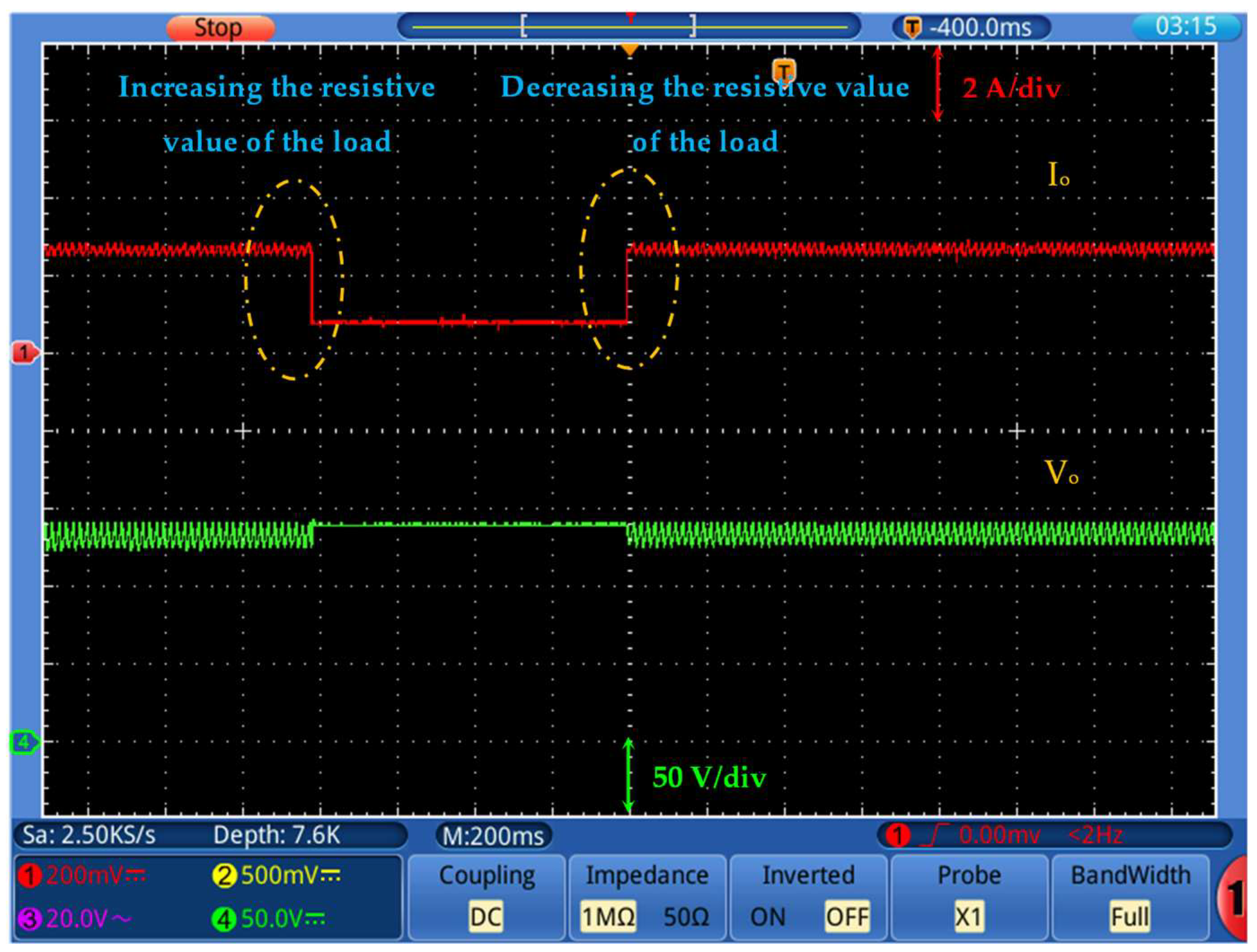
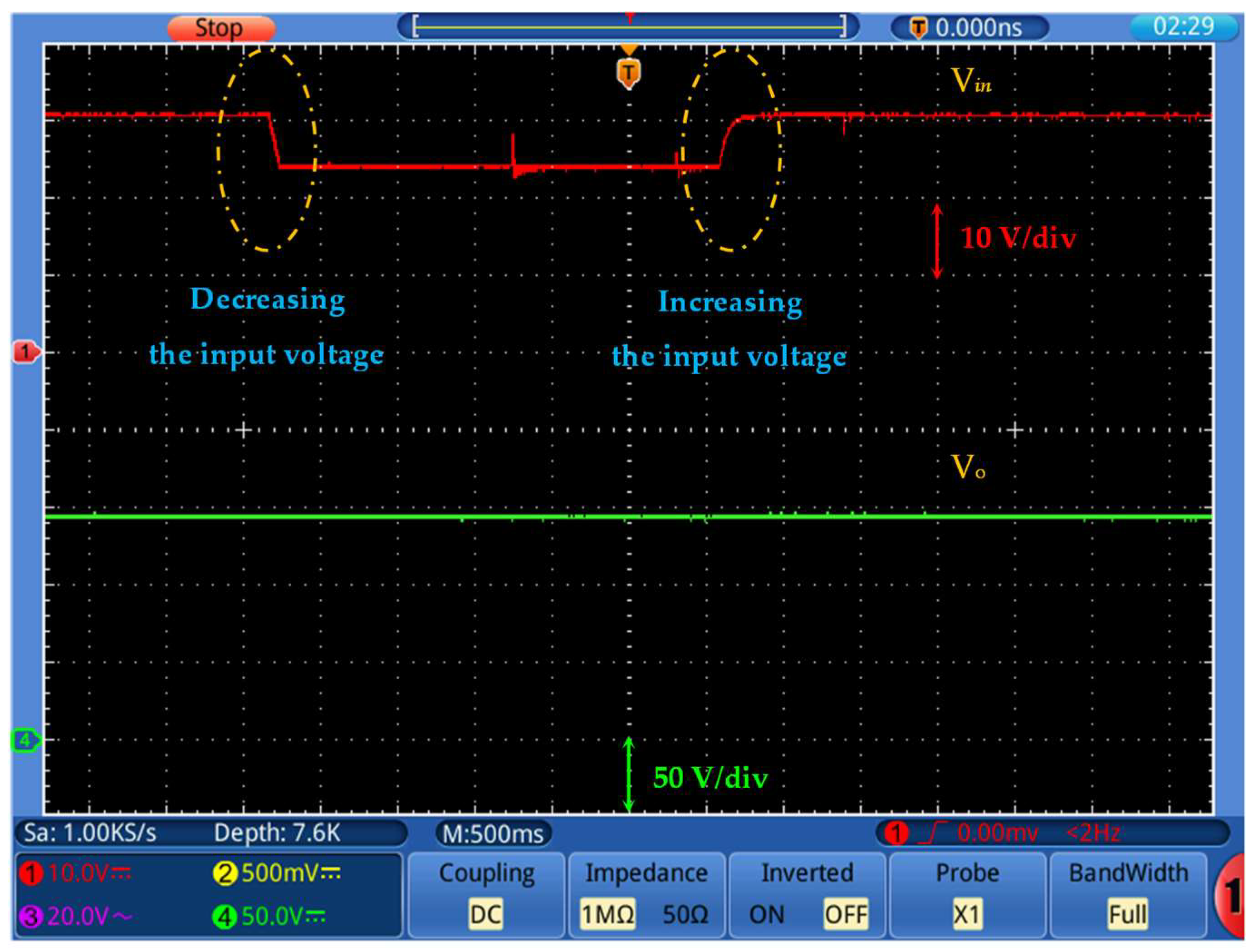
8. Closed-Loop Performance
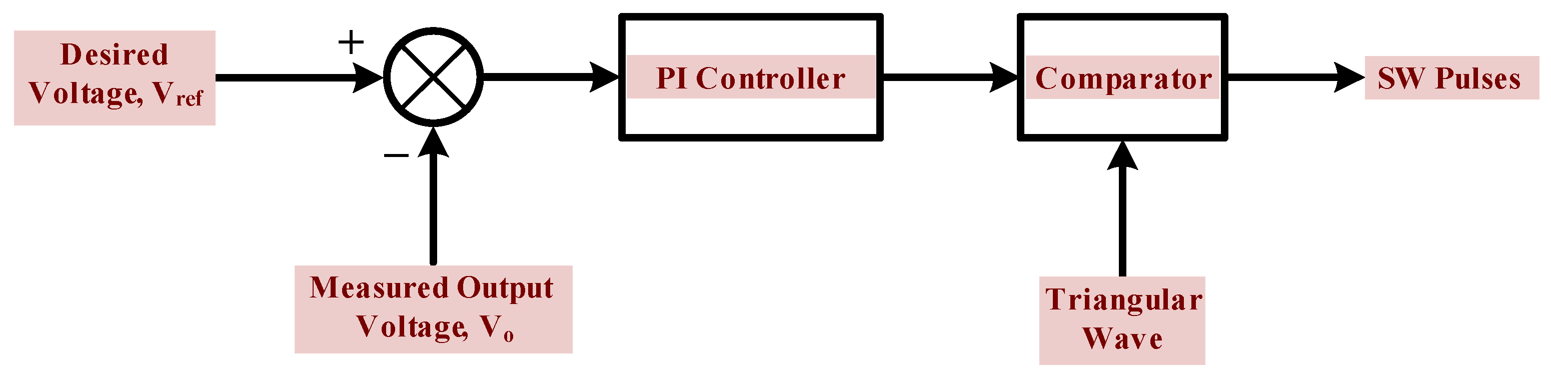
The experimental prototype of the proposed multicell converter (n = 2) is also examined during a closed-loop control. Converter stability and dynamic performance need to be improved by designing the PI controller. Consequently, the phase and gain margins by designing a robust feedback (closed-loop) controller are properly selected. A schematic diagram of the circuit that is utilized to control the output voltage of the proposed converter is shown in Figure 12.

8.1. PI Controller

The transfer function of the PI controller is given as
G P I s = K P   s + K I s
where KP and KI are the parameters of the PI controller. To obtain a stable and well-regulated DC-DC converter, the phase margin of the controlled converter should be greater than 45° [41]. A higher phase margin enhances the transient performance of the converter. A PI controller is designed to regulate the output voltage of the multi-cell DC-DC boost converter against load, input voltage, and reference voltage variations. The PI controller parameters are selected based on the stability analysis using the frequency response technique. The proportional (KP) and integral (KI) gains of the PI controller are selected to be KP = 0.001 and KI = 0.4 based on the required phase margin of 96.8° and gain margin of 15.3 dB. Figure 13 displays a bode plot of the closed-loop system with the designed PI controller. It is clear from the figure that the designed closed-loop control system is stable.

8.2. Closed-Loop Results

The experimental responses of the proposed multicell converter (n = 2) during closed-loop control are captured. Figure 14 shows the output voltage response starting with changing the reference voltage (Vref) to 150 V at Vin = 24 V. It is observed that the output voltage signal has a good dynamic response and tracks the reference voltage smoothly without overshoots and undershoots. To examine the robustness of the closed-loop control of the proposed multicell converter (n = 2), Figure 15 demonstrates the output voltage and current responses by changing the resistive value of the load at Vref = 140 V. Figure 16 presents the output voltage response at Vref= 145 V by changing the input voltage (Vin) from 31 V → 24 V → 31 V. As obvious, the output voltage signal has a good dynamic response. Also, Figure 17 shows the output voltage response at Vin = 24 V by changing the reference voltage (Vref) from 125 V → 115 V. The output voltage response tracks the reference voltage smoothly.

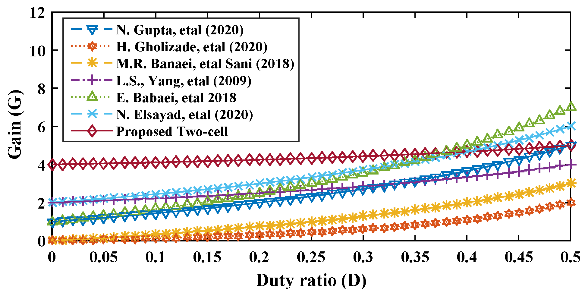
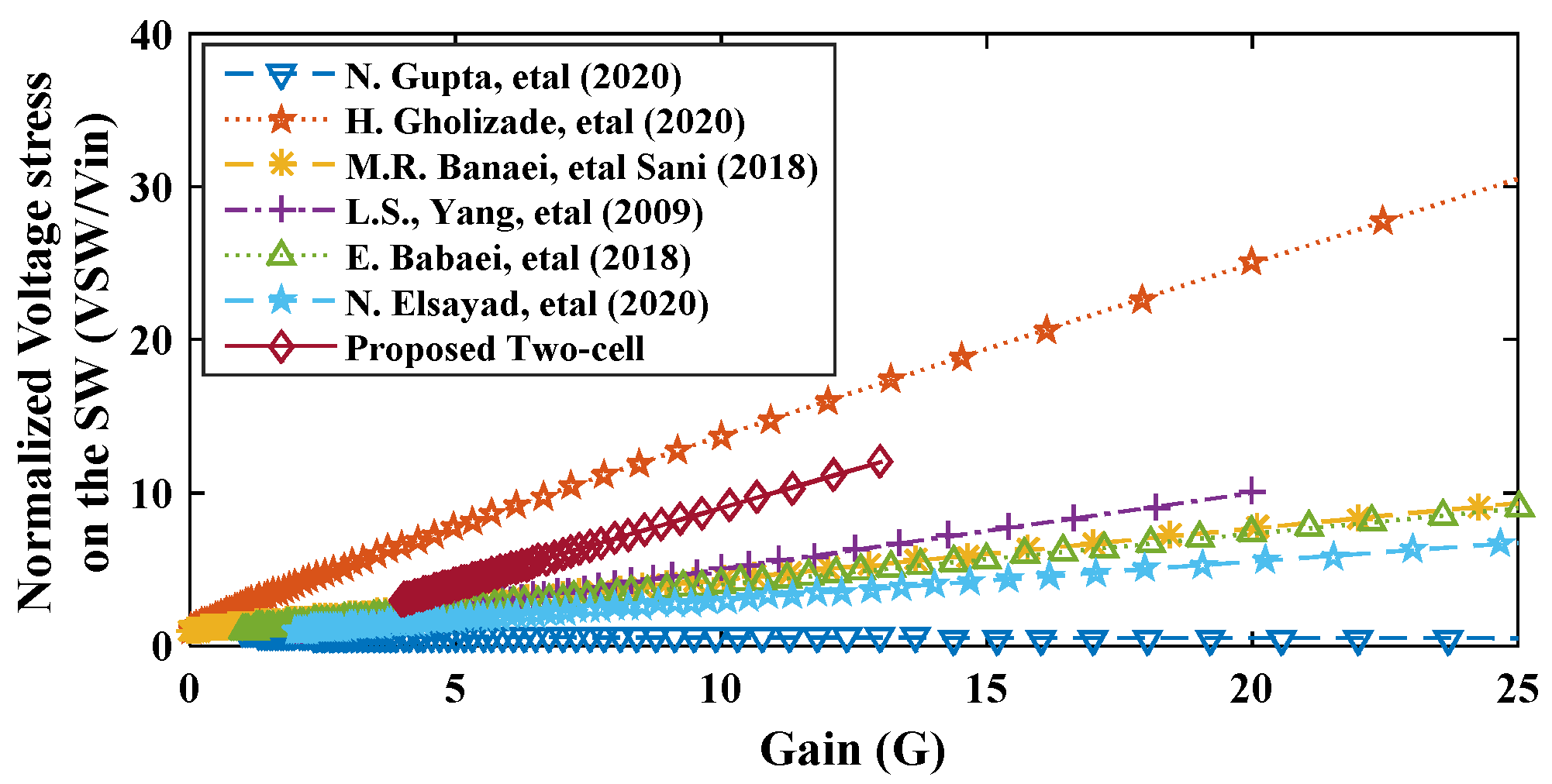
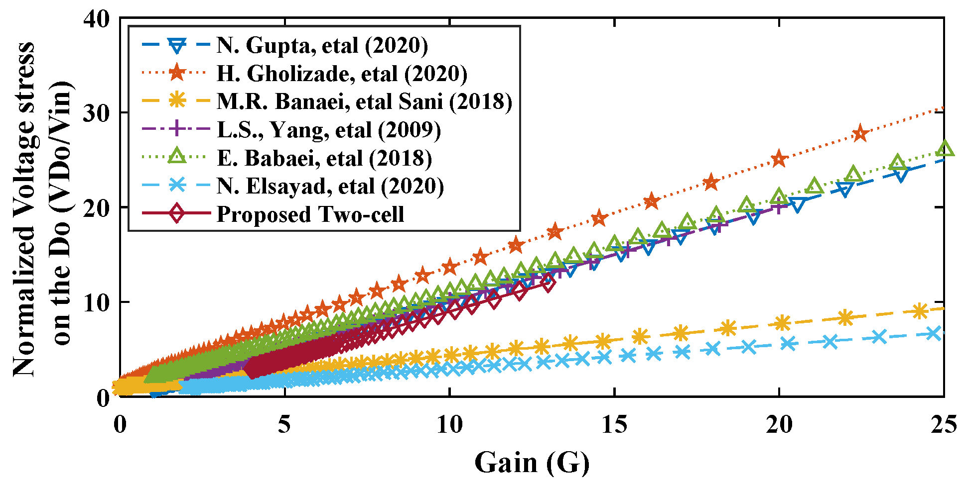
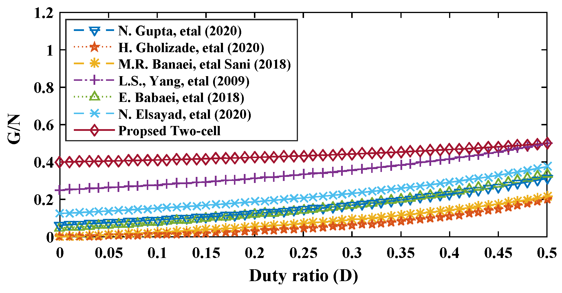
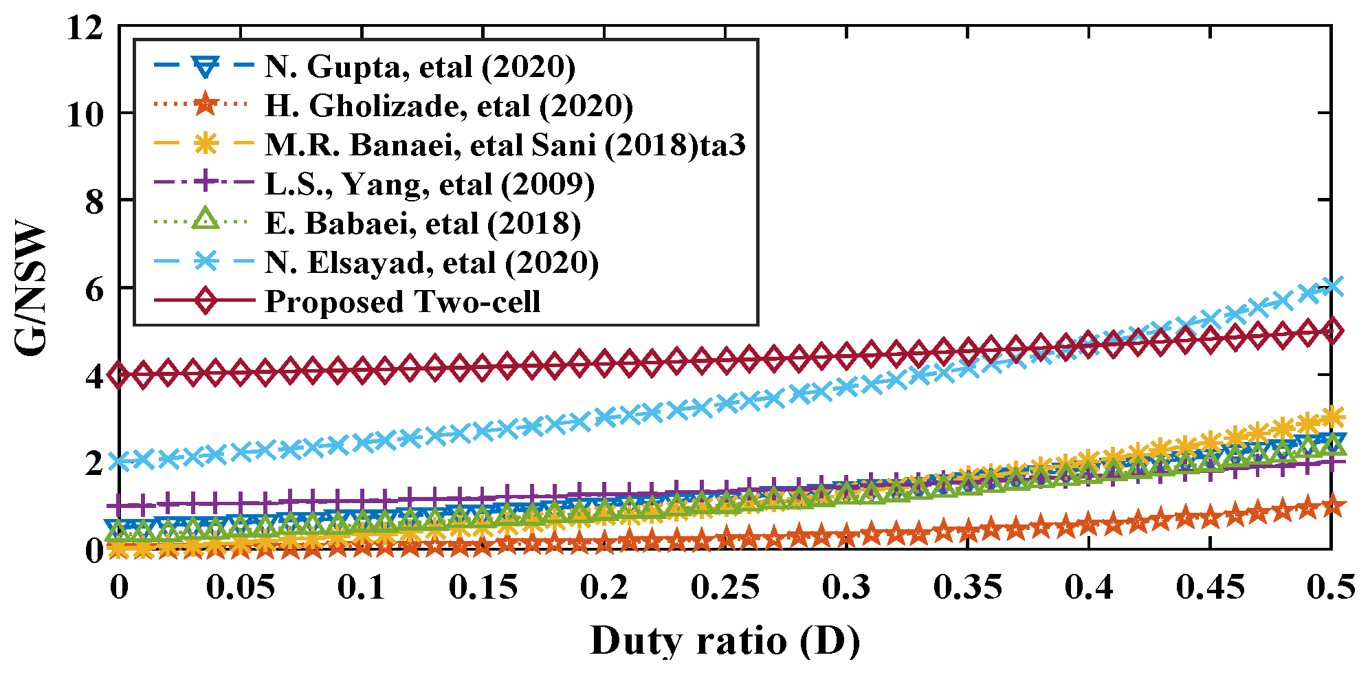
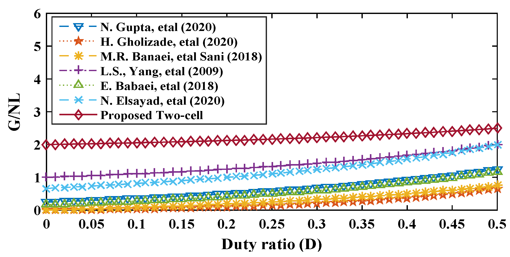
9. Comparison with Recent Converters

To evaluate the effectiveness of the single-switch high-gain multicell boost DC-DC converter, a comprehensive comparison between the proposed converter and previous boost converters is provided, as shown in Table 2. The number of components, which include switches, inductors, diodes, and capacitors, are presented for the proposed and other converters. It is obvious that the proposed converter has a smaller number of components compared to previous converters [25,27,29,30] and has an identical number of components as that reported in [26], and more than that in [28], which has the smaller count. Therefore, this converter topology structure contributes to a cost-effective system that is compact and lightweight compared to other topologies.
The table below also shows the relationships between the duty ratio (D) and voltage gain (G), normalized voltage stress on the SW ( V S W / V i n ), normalized voltage stress on the Do ( V D o / V i n ), Fs (KHz), open/closed loop, control method, experimental efficiency at 100 W, and G at D = 0.4 for the proposed and other converter topologies. It can be seen that the voltage gain (G) at D = 0.4 gives a higher gain compared to previous works and is identical to that of the converter in [30]. However, the converter in [30] has a larger number of components compared to the proposed converter.
To provide deeper insight into, and analysis of, the proposed converter and previous converter works, Figure 18, Figure 19, Figure 20, Figure 21, Figure 22, Figure 23, Figure 24 and Figure 25 show plots based on the data in Table 2. In Figure 18, the voltage gain (G) under duty ratio changes (D) for the proposed converter and the prior converter topologies are plotted. As obvious, the proposed converter boasts a higher voltage gain compared to previous boosting converters for D ≤ 0.4. Additionally, the proposed converter demonstrates superior voltage gain even at very low duty cycles. This indicates that the suggested boost converter experiences lower switching and conduction losses, resulting in higher efficiency.
Figure 19 shows the normalized voltage stress on the SW ( V S W / V i n ) versus the voltage gain. It is observed that the SW in the proposed converter experiences good voltage stress at high voltage gain compared to the power switches in previous converters. It can be seen that the previous converter topologies with low voltage stress have a large number of components, as in [25,27,29,30]. Additionally, the proposed converter topology has a reasonable voltage stress compared to the converters in [26,28], which have nearly the same number of components. In Figure 20, the voltage stress on the diode in the proposed converter has a moderate value compared to the diodes in the previous converters. This comparison proves the improved performance of the proposed converter and stress reduction.
In Figure 21, Figure 22, Figure 23, Figure 24 and Figure 25, the duty ratio is plotted versus gain to total component count ratio (G/N), gain to switch count ratio (G/NSW), gain to diode count ratio (G/ND), gain to diode count ratio (G/ND), gain to inductor count ratio (G/NL), and gain to capacitor count ratio (G/NC) for the proposed converter and the prior converter works. As is obvious, the proposed converter exhibits higher gain compared to previous converters concerning the number of components. The proposed converter shows a higher gain compared to previous converter works, particularly for D ≤ 0.5.
Therefore, the proposed converter is appropriate for renewable energy applications that require variable and constant high output voltage with a wider range of duty ratios. This converter topology structure contributes to a cost-effective system that is compact and lightweight compared with other topologies. It compromises between the required performance, the low number of components, low voltage stress on the components, high efficiency, and cost-effectiveness.

10. Conclusions

This paper presented the state space average model of a new single-switch multicell high-gain boost DC-DC converter considering the series parasitic resistances of the passive elements operating in CCM. Based on the state space average model, a small signal model of the proposed converter was introduced. The control-to-input and input-to-output open-loop transfer functions of the offered converter have been derived and presented. The behavior of the proposed topology based on the state space average model was obtained using Matlab R2023b software. The stability analysis of the suggested topology using a bode plot and root locus diagrams was investigated. The PI controller parameters for closed-loop control of the proposed converter were designed. Simulation results of the converter state space average model have been verified by comparing with the corresponding experimental results for actual hardware of the proposed converter with two cells for open-loop and closed-loop operations. It was found that the derived state space average and small signal models of the proposed multicell boost converter are convenient and accurate. These developed models can be considered as effective tools for studying dynamic performance, investigating stability, and designing control of the proposed converter. Based on the experimental results, the proposed converter has a fast dynamic response during starting, load change, input voltage, and reference voltage variations. A comprehensive comparison between the proposed converter and previous converters found that the proposed converter exhibits higher gain compared to previous converters with respect to the number of components. This converter’s topology contributes to a cost-effective system that is compact and lightweight compared with other topologies. It compromises between the required performance, the low number of components, low voltage stress on the components, and cost-effectiveness.

Author Contributions

S.A.D. and A.S.M. contributed to the study design and implementation, as well as the data analysis and paper writing. Writing—review and editing, S.A.D., A.S.M. and M.S.Z.; visualization, M.S.Z. and K.B.T. The published version of the work has been reviewed and approved by all authors. All authors have read and agreed to the published version of the manuscript.

Funding

The authors extend their appreciation to the Deanship of Scientific Research at Northern Border University, Arar, KSA for funding this research work through the project number “NBU-FFR-2024-1250-01”, and also to Khalifa University, Abu Dhabi, United Arab Emirates, under Award No. KAU-KU-2021-01.

Institutional Review Board Statement

Not applicable.

Informed Consent Statement

Not applicable.

Data Availability Statement

Data are contained within the article.

Conflicts of Interest

The authors declare no conflict of interest.

References

  1. Alkhaldi, A.; Elkhateb, A.; Laverty, D. Voltage Lifting Techniques for Non-Isolated DC/DC Converters. Electronics 2023, 12, 718. [Google Scholar] [CrossRef]
  2. Zhang, C.; Xu, B.; Jasni, J.; Radzi, M.A.M.; Azis, N.; Zhang, Q. Model Control and Digital Implementation of the Three Phase Interleaved Parallel Bidirectional Buck–Boost Converter for New Energy Electric Vehicles. Energies 2022, 15, 7178. [Google Scholar] [CrossRef]
  3. Chen, J.; Hu, H.; Wang, M.; Ge, Y.; Wang, K.; Huang, Y.; Yang, K.; He, Z.; Xu, Z.; Li, Y.R. Power Flow Control-Based Regenerative Braking Energy Utilization in AC Electrified Railways: Review and Future Trends. IEEE Trans. Intell. Transp. Syst. 2024, 25, 6345–6365. [Google Scholar] [CrossRef]
  4. Elbarbary, Z.M.S.; Cheema, K.M.; Al-Gahtani, S.F.; El-Sehiemy, R.A. High gain chopper supplied from PV system to fed synchronous reluctance motor drive for pumping water application. Sci. Rep. 2022, 12, 15519. [Google Scholar] [CrossRef]
  5. Tahami, H.; Akbari, E.; Mohammed, A.H.; Faraji, R.; Channumsin, S. A Transformerless Enhanced-Boost Quasi-Z-Source Inverter with Low Input Current Ripple for Stand-Alone RES-Based Systems. Energies 2023, 16, 2611. [Google Scholar] [CrossRef]
  6. Mumtaz, F.; Yahaya, N.Z.; Meraj, S.T.; Singh, N.S.S.; Abro, G.E.M. A Novel Non-Isolated High-Gain Non-Inverting Interleaved DC–DC Converter. Micromachines 2023, 14, 585. [Google Scholar] [CrossRef] [PubMed]
  7. Li, S.; Haskew, T.A.; Li, D.; Hu, F. Integrating photovoltaic and power converter characteristics for energy extraction study of solar PV systems,” Renewable Energy. Renew. Energy 2011, 36, 3238–3245. [Google Scholar] [CrossRef]
  8. Gules, R.; Pfitscher, L.L.; Franco, L.C. An Interleaved Boost DC-DC Converter with Large Conversion Ratio. In Proceedings of the IEEE International Symposium on Industrial Electronics, Rio de Janeiro, Brazil, 9–11 June 2003; Volume 1, pp. 411–416. [Google Scholar] [CrossRef]
  9. Yao, G.; Chen, A.; He, X. Soft Switching Circuit for Interleaved Boost Converters. IEEE Trans. Power Electron. 2007, 22, 80–86. [Google Scholar] [CrossRef]
  10. Ismail, E.H.; Al-Saffar, M.A.; Sabzali, A.J.; Fardoun, A.A. A Family of Single-Switch PWM Converters with High Step-Up Conversion Ratio. IEEE Trans. Circuits Syst.—I Regul. Pap. 2008, 55, 1159–1171. [Google Scholar] [CrossRef]
  11. Axelrod, B.; Berkovich, Y.; Ioinovici, A. Switched-Capacitor/Switched-Inductor Structures for Getting Transformerless Hybrid DC–DC PWM Converters. IEEE Trans. Circuits Syst.—I Regul. Pap. 2008, 55, 687–696. [Google Scholar] [CrossRef]
  12. Yang, P.; Xu, J.; Zhou, G.; Zhang, S. A New Quadratic Boost Converter with High Voltage Step-up Ratio and Reduced Voltage Stress. In Proceedings of the IEEE 7th International Power Electronics and Motion Control Conference—ECCE Asia, Harbin, China, 2–5 June 2012; pp. 1–6. [Google Scholar] [CrossRef]
  13. Algamluoli, A.F.; Wu, X. A New Single-Cell Hybrid Inductor-Capacitor DC-DC Converter for Ultra-High Voltage Gain in Renewable Energy Applications. Electronics 2023, 12, 3101. [Google Scholar] [CrossRef]
  14. Alilou, S.M.; Maalandish, M.; Samadian, A.; Abolhassani, P.; Hosseini, S.H.; Khooban, M.-H. A new high step-up DC-DC converter using voltage lift techniques suitable for renewable applications. CSEE J. Power Energy Syst. 2023, 1–10, (early access). [Google Scholar]
  15. Mansour, A.S.; Sarhan, E.M.; El-Sabbe, A.E.; Osheba, D.S.M. A Single-switch Non-isolated High Gain DC/DC Converter for PV Applications. Eng. Res. J. 2022, 45, 261–271. [Google Scholar] [CrossRef]
  16. Mansour, A.S.; Amer, A.H.; El-Kholy, E.E.; Zaky, M.S. High gain DC/DC converter with continuous input current for renewable energy applications. Sci. Rep. 2022, 12, 12138. [Google Scholar] [CrossRef]
  17. Zaid, M.; Malick, I.H.; Ashraf, I.; Tariq, M.; Alamri, B.; Rodrigues, E.M.G. A Nonisolated Transformerless High-Gain DC–DC Converter for Renewable Energy Applications. Electronics 2022, 11, 2014. [Google Scholar] [CrossRef]
  18. Gholizadeh, H.; Ben-Brahim, L. A New Non-Isolated High-Gain Single-Switch DC–DC Converter Topology with a Continuous Input Current. Electronics 2022, 11, 2900. [Google Scholar] [CrossRef]
  19. Mirzaei, A.; Rezvanyvardom, M.; Najafi, E. A fully soft switched high step-up SEPIC-boost DC-DC converter with one auxiliary switch. Int. J. Circuit Theory Appl. 2019, 47, 427–444. [Google Scholar] [CrossRef]
  20. Patidar, K.; Umarikar, A.C. High step-up pulse-width modulation DC–DC converter based on quasi-Z-source topology. IET Power Electron. 2015, 8, 477–488. [Google Scholar] [CrossRef]
  21. Siwakoti, Y.P.; Blaabjerg, F.; Loh, P.C. Quasi Y-Source Boost DC-DC Converter. IEEE Trans. Power Electron. 2015, 30, 6514–6519. [Google Scholar] [CrossRef]
  22. Zhao, J.; Chen, D.; Jiang, J. Transformerless High Step-Up DC-DC Converter with Low Voltage Stress for Fuel Cells. IEEE Access 2021, 9, 10228–10238. [Google Scholar] [CrossRef]
  23. Salehi, N.; Martínez-García, H.; Velasco-Quesada, G. Modified Cascaded Z-Source High Step-Up Boost Converter. Electronics 2020, 9, 1932. [Google Scholar] [CrossRef]
  24. Nouri, T.; Hosseini, S.H.; Babaei, E. Analysis of voltage and current stresses of a generalised step-up DC–DC converter. IET Power Electron. 2014, 7, 1347–1361. [Google Scholar] [CrossRef]
  25. Gupta, N.; Bhaskar, M.S.; Almakhles, D.; Sanjeevikumar, P.; Subramaniam, U.; Leonowicz, Z.; Mitolo, M. Novel non-isolated quad-switched inductor double-switch converter for DC microgrid application. In Proceedings of the IEEE International Conference on Environment and Electrical Engineering and IEEE Industrial and Commercial Power Systems Europe (EEEIC/I&CPS Europe), Madrid, Spain, 9–12 June 2020; pp. 1–6. [Google Scholar] [CrossRef]
  26. Gholizade, H.; Aboufazeli, S.; Rafiee, Z.; Afjei, E.; Hamzeh, M. A non-isolated high gain DC–DC converters with positive output voltage and reduced current stresses. In Proceedings of the IEEE 11th Power Electronics, Drive Systems, and Technologies Conference, Tehran, Iran, 4–6 February 2020; pp. 1–6. [Google Scholar] [CrossRef]
  27. Banaei, M.R.; Sani, S.G. Analysis and implementation of a new SEPIC based single switch buck-boost DC–DC converter with continuous input current. IEEE Trans. Power Electron. 2018, 33, 10317–10325. [Google Scholar] [CrossRef]
  28. Yang, L.S.; Liang, T.J.; Chen, J.F. Transformerless DC–DC converters with high step-up voltage gain. IEEE Trans. Industr. Electron. 2009, 56, 3144–3152. [Google Scholar] [CrossRef]
  29. Babaei, E.; Maheri, H.M.; Sabahi, M.; Hosseini, S.H. Extendable nonisolated high gain DC–DC converter based on active–passive inductor cells. IEEE Trans. Ind. Electron. 2018, 65, 9478–9487. [Google Scholar] [CrossRef]
  30. Elsayad, N.; Moradisizkoohi, H.; Mohammed, O. A new SEPIC-based step-up DC-DC converter with wide conversion ratio for fuel cell vehicles: Analysis and design. IEEE Trans. Ind. Electron. 2020, 68, 6390–6400. [Google Scholar] [CrossRef]
  31. Mansour, A.S.; Zaky, M.S. A new extended single-switch high gain DC–DC boost converter for renewable energy applications. Sci. Rep. 2023, 13, 264. [Google Scholar] [CrossRef] [PubMed]
  32. Das, H.S.; Li, Z.; Li, S.; Dong, W. Small Signal Modeling, Control and Experimentation of Boost Converter Including Parasitic Elements. J. Control Autom. Electr. Syst. 2021, 32, 956–967. [Google Scholar] [CrossRef]
  33. Deraz, S.A.; Azazi, H.Z.; Zaky, M.S.; Metwaly, M.K.; Dessouki, M.E. Performance Investigation of Three-Phase Three-Switch Direct PWM AC/AC Voltage Converters. IEEE Access 2019, 7, 11485–11501. [Google Scholar] [CrossRef]
  34. Alajmi, B.N.; Ahmed, N.A.; Al-Othman, A.K. Small-signal analysis and control implementation of boost converter fed PMDC motor for electric vehicle applications. J. Eng. Res. 2021, 9, 189–208. [Google Scholar] [CrossRef]
  35. Abdel-Gawad, H.; Sood, V.K. Small-Signal Analysis of Boost Converter, including Parasitics, operating in CCM. In Proceedings of the 6th IEEE Power India International Conference (PIICON), Delhi, India, 5–7 December 2014; pp. 1–5. [Google Scholar] [CrossRef]
  36. Khatun, K.; Ratnam, V.V.; Rathore, A.K.; Narasimharaju, B.L. Small-Signal Analysis and Control of Soft-Switching Naturally Clamped Snubberless Current-Fed Half-Bridge DC/DC Converter. Appl. Sci. 2020, 10, 6130. [Google Scholar] [CrossRef]
  37. Górecki, P. Electrothermal Averaged Model of a Diode–IGBT Switch for a Fast Analysis of DC–DC Converters. IEEE Trans-Actions Power Electron. 2022, 37, 13003–13013. [Google Scholar] [CrossRef]
  38. Górecki, P.; d’Alessandro, V. A Datasheet-Driven Electrothermal Averaged Model of a Diode–MOSFET Switch for Fast Sim-ulations of DC–DC Converters. Electronics 2024, 13, 154. [Google Scholar] [CrossRef]
  39. Ayachit, A.; Kazimierczuk, M.K. Averaged Small-Signal Model of PWM DC-DC Converters in CCM Including Switching Power Loss. IEEE Trans. Circuits Syst. II Express Briefs 2019, 66, 262–266. [Google Scholar] [CrossRef]
  40. Zhang, Y.; Dong, Z.; Liu, J.; Ma, X.; Li, X.; Han, J. Modeling and controller design of high voltage gain DC-DC converter with multi-cell diode-capacitor network. In Proceedings of the IEEE 8th International Power Electronics and Motion Control Conference (IPEMC-ECCE Asia), Hefei, China, 22–26 May 2016; pp. 3066–3072. [Google Scholar] [CrossRef]
  41. Garg, M.M.; Hote, Y.V.; Pathak, M.K. Design and Performance Analysis of a PWM dc–dc Buck Converter Using PI–Lead Compensator. Arab. J. Sci. Eng. 2015, 40, 3607–3626. [Google Scholar] [CrossRef]
Figure 1. Single-stage multicell boost DC-DC converter with parasitic series resistances of the passive elements.
Electronics 13 03264 g001
Figure 2. On state equivalent circuit of the proposed multicell converter: (a) active and inactive components, and (b) analogous electrical circuit.
Electronics 13 03264 g002
Figure 3. Off-state equivalent circuit of the proposed multicell converter: (a) active and inactive components, and (b) analogous electrical circuit.
Electronics 13 03264 g003
Figure 4. Bode plot diagram of the open-loop control-to-output transfer function of the proposed multicell converter (n = 2).
Electronics 13 03264 g004
Figure 5. Root locus diagram of the open-loop control-to-output transfer function of the proposed multicell converter (n = 2).
Electronics 13 03264 g005
Figure 6. Bode plot diagram of the open-loop input-to-output transfer function of the proposed multicell converter (n = 2).
Electronics 13 03264 g006
Figure 7. Root locus diagram of the open-loop input-to-output transfer function of the proposed multicell converter (n = 2).
Electronics 13 03264 g007
Figure 8. Actual photos of the experimental setup system components for open-loop and closed-loop operations.
Electronics 13 03264 g008
Figure 9. The schematic diagram for the experimental setup system for open-loop and closed-loop operations.
Electronics 13 03264 g009
Figure 10. Open-loop performance of the proposed multicell converter (n = 2) when the input voltage Vin = 24 V, D = 0.5, and Fs = 5 kHz: (a,c,e) experimental and (b,d,f) simulation results based on the SSAM.
Electronics 13 03264 g010aElectronics 13 03264 g010b
Figure 11. Open-loop performance of the proposed multicell converter (n = 2) when the input voltage Vin = 24 V, D = 0.6, and Fs = 5 kHz: (a,c,e) experimental and (b,d,f) simulation results based on the SSAM.
Electronics 13 03264 g011aElectronics 13 03264 g011b
Figure 12. A schematic graph of a closed-loop control circuit with PI controller.
Electronics 13 03264 g012
Figure 13. Bode plot diagram of the closed-loop control system of the proposed multicell converter (n = 2) with the designed PI controller based on stability analysis.
Electronics 13 03264 g013
Figure 14. Output voltage response starting with changing the reference voltage (Vref) to 150 V at Vin = 24 V.
Electronics 13 03264 g014
Figure 15. Output voltage and current responses with the load variation at Vref = 140 V.
Electronics 13 03264 g015
Figure 16. Output voltage response at Vref = 145 V by changing the input voltage (Vin) from 31 V → 24 V → 31 V.
Electronics 13 03264 g016
Figure 17. Output voltage response at Vin = 24 V by changing the desired voltage (Vref) from 125 V → 115 V.
Electronics 13 03264 g017
Figure 18. Voltage gain versus duty ratio.
Electronics 13 03264 g018
Figure 19. Normalized voltage stress on the SW ( V S W / V i n ) versus gain.
Electronics 13 03264 g019
Figure 20. Normalized voltage stress on the Do ( V D o / V i n ) versus gain.
Electronics 13 03264 g020
Figure 21. Gain to total component count ratio (G/N) versus duty cycle.
Electronics 13 03264 g021
Figure 22. Gain to switch count ratio (G/NSW) versus duty cycle.
Electronics 13 03264 g022
Figure 23. Gain to diode count ratio (G/ND) versus duty cycle.
Electronics 13 03264 g023
Figure 24. Gain to inductor count ratio (G/NL) versus duty cycle.
Electronics 13 03264 g024
Figure 25. Gain to capacitor count ratio (G/NC) versus duty cycle.
Electronics 13 03264 g025
Table 1. Parameters of the proposed single-switch two-cell boost converter.
ParameterValue
Vin24 V
Vo132 V
rLi0.64 Ω
Li1.7 mH
rCi0.12 Ω
Ci47 µF
rCo0.12 Ω
Co47 µF
Fs5 kHz
R130 Ω
DiodesMUR1560
Main switch (SW)FGH40N60UFD
Table 2. Comparison between the two-cell proposed converter and recent topologies.
ItemRef. [25]Ref. [26]Ref. [27]Ref. [28]Ref. [29]Ref. [30]The Proposed
n = 2
Switch, SW2212311
Inductor, L4342632
Capacitor, C1362173
Diode, D92321154
Total Component Count1610148211610
Gain, G ( 1 + 3   D ) ( 1 D ) D ( 1 D ) 2 3   D ( 1 D ) 2 ( 1 D ) ( 1 + 5   D ) ( 1 D ) ( 2 + 2   D ) ( 1 D ) ( 4 3   D ) ( 1 D )
Normalized   Voltage   Stress   on   the   SW   ( V S W / V i n ) ( G + 1 ) 2   G G D ( G + 3 ) 3 G 2 ( G + 2 ) 3 ( G + 2 ) 4 ( G 1 )
Normalized   Voltage   Stress   on   the   D o   ( V D o / V i n ) G G D ( G + 3 ) 3 G ( G + 1 ) ( G + 2 ) 4 ( G 1 )
Fs (KHz)506033100201005
Open/Closed LoopOpen-loopOpen-loopOpen-loopOpen-loopOpen/Closed-loopOpen/Closed-loopOpen/Closed-loop
Control Methodn/an/an/an/aPI ControllerType III voltage controllerPI Controller
Exp. Efficiency (%) Pout = 100 Wn/an/a939295.692.196
Type of LoadGroundedGroundedGroundedGroundedFloatingFloatingGrounded
G at D = 0.43.671.1123.3354.674.67
Disclaimer/Publisher’s Note: The statements, opinions and data contained in all publications are solely those of the individual author(s) and contributor(s) and not of MDPI and/or the editor(s). MDPI and/or the editor(s) disclaim responsibility for any injury to people or property resulting from any ideas, methods, instructions or products referred to in the content.

