Article

A High-Quality and Space-Efficient Design for Memristor Emulation

Department of Electronics and Communication Engineering, Jaypee Institute of Information Technology, Noida 201304, India
*
Author to whom correspondence should be addressed.
Electronics 2024, 13(16), 3331; https://doi.org/10.3390/electronics13163331 (registering DOI)
Submission received: 29 July 2024 / Revised: 16 August 2024 / Accepted: 19 August 2024 / Published: 22 August 2024
(This article belongs to the Section Circuit and Signal Processing)

Abstract

:
The paper presents a new design for a compact memristor emulator that uses a single active component and a grounded capacitor. This design incorporates a current backward transconductance amplifier as the active element, enabling the emulation of both grounded and floating memristors in incremental and decremental modes. The paper provides an in-depth analysis of the circuit, covering ideal, non-ideal, and parasitic factors. The theoretical performance of the memristor emulator is confirmed through post-layout simulations with 180 nm generic process design kit (gpdk) technology, demonstrating its capability to operate at low voltages (±1 V) with minimal power consumption. Additionally, the emulator shows strong performance under variations in process, voltage, and temperature (PVT) and functions effectively at a frequency of 2 MHz. Experimental validation using commercially available integrated circuits further supports the proposed design.

1. Introduction

Since the inception of the memristor [1,2], there has been a notable surge in its integration into analog signal processing. This increase has driven a growing interest in pioneering memristor-based designs, leading to significant advances in signal processing. Particularly noteworthy is the significant headway in utilizing memristors as emulators, revolutionizing fundamental design approaches. Numerous emulator designs leveraging memristors have emerged, boasting remarkable enhancements in circuit simplicity, operational frequency, real-time performance, power efficiency, and other crucial aspects.
With the substantial growth in designs centered on memristor emulators (Mes), there is now a plethora of these Mes documented in the literature, providing designers with a great deal of versatility [3,4,5,6,7,8,9,10,11,12,13,14,15,16,17,18,19,20,21,22,23,24,25,26,27,28,29,30,31,32]. Some reported designs exclusively utilize passive components for realization [3,4,5]. It is noteworthy that the first notable work on passive ME is documented in [3]. Conversely, designs outlined in [6,7,8,9,10,11,12,13,14,15,16,17,18,19,20,21,22,23,24,25,26,27,28,29,30,31,32] rely on active building block(s). Researchers have also shown interest in further realizing higher-order memelements like meminductors and memcapacitors [33,34,35]. This study identifies, summarizes, and compares the most pertinent works on memristors, delineating proposed ideas based on numerous key performance attributes of significant importance.
The ME circuits outlined In various references [6,7,8,9,12,13,16,17,18,23,24] rely on analog multipliers for their design, resulting in increased circuit complexity and power consumption. However, the proposed ME circuit offers a solution by eliminating the need for an analog multiplier, thereby simplifying the overall circuitry. Furthermore, compared to existing Mes in [6,7,8,9,10,13,15,16,17,18,19,21,22,23,24,26,27,28,31,32], the proposed ME circuit has a higher operational frequency. Unlike previous ME designs documented in [6,7,8,9,10,11,12,13,15,16,17,18,19,21,23,24,26,27,29,30,31,32], which often incorporate two or more passive components and are not resistorless, the proposed ME circuit achieves a streamlined design by utilizing only a single capacitor and offers resistorless design. Additionally, while prior ME circuits [6,7,8,9,10,11,12,13,14,15,16,17,18,19,20,21,23,24,26,27,29,30,32] exclusively focus on either grounded or floating structures, this work introduces both grounded and floating ME configurations. Furthermore, while the ME circuits in [8,10,19,32] typically achieve either decremental or incremental functionality, the proposed ME circuit offers the unique capability to realize both decremental and incremental characteristics within the same circuit structure, eliminating the need for additional switches.
The above classifications highlight the limitations of existing circuits. To address these issues, this study introduces an innovative memristor emulator with MOS-C realization only, aiming to achieve diverse functions. The proposed design makes use of a single current backward transconductance amplifier (CBTA) and a grounded capacitor only, leading to a simpler configuration. The grounded and floating memristors can be realized in both incremental and decremental configurations with the proposed design. The study includes a comprehensive examination of ideal and non-ideal scenarios to emphasize the real-time performance of the suggested ME. Performance validation under variations in process, voltage, and temperature is carried out through Monte Carlo analysis. Furthermore, experimental verifications have been incorporated.

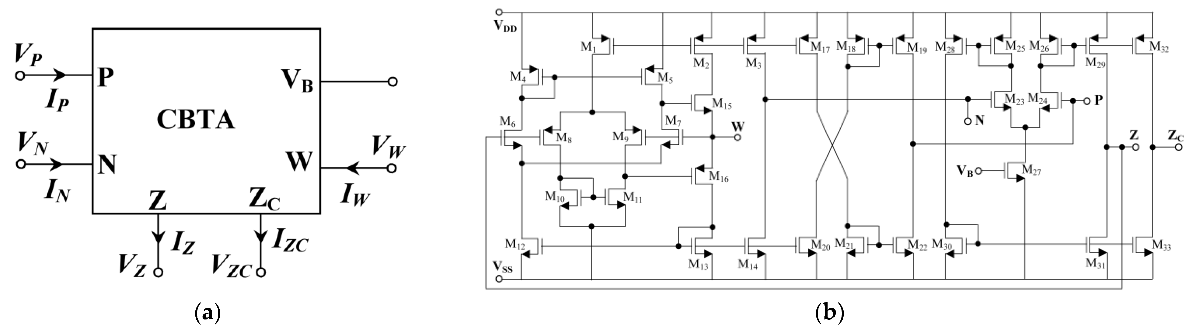
2. CBTA Symbol and CMOS Realization

The active element CBTA is a versatile element featuring a combination of a dual-output second-generation current conveyor and a transconductance amplifier [36]. The use of a transconductance amplifier in any active element introduces an electronic tunability feature, allowing for precise control of circuit parameters [37,38,39]. A symbolic representation of the CBTA is illustrated in Figure 1a, while its CMOS implementation is depicted in Figure 1b. The terminal attributes of CBTA are defined as given below.
I Z = g m V P V N , I Z C = g m V P V N ,   V W = V Z ,   I P = I W ,   I N = I W
where, IZ, IZC, IP, IN and IW are the currents at Z, ZC, P, N and W terminals, respectively; VP, VN, VZ and VW are the voltages at P, N, Z and W terminals, respectively, and g m is the transconductance of CBTA. The transconductance ( g m ) of the CBTA in (1) is expressed as shown below:
g m = K V B V S S V T H
where K = μ n C O X 2 W L M i (i = 23, 24, 27) and W L M 23 = W L M 24 = W L M 27 ; μn and COX are the mobility of electron and gate oxide capacitance per unit area. In (2), VB, VSS, and VTH are the bias voltage of the CBTA, the negative supply voltage, and the threshold voltage of the MOS transistor, respectively. It is observed from (2) that the transconductance ( g m ) can be adjusted through the bias voltage, VB.
The CBTA’s terminal attributes are described as follows by considering non-idealities.
I Z = γ 1 g m V P V N ,   I Z C = γ 2 g m V P V N ,   V W = β V Z ,   I P = α 1 I W ,   I N = α 2 I W
where γ 1 and γ 2 are transconductance inaccuracies, β is the non-ideal voltage transfer gain and α is the non-ideal current transfer gain.
A parasitic model of the CBTA is depicted in Figure 2. In the CBTA, the terminals P, N, Z, and ZC are high impedance terminals and terminal W is a low impedance terminal. The high-impedance terminals exhibit a parallel combination of an internal resistor and capacitor such that Zi = Ri//(1/sCi) (where I = P, N, Z and ZC). A small series resistance RW appears at terminal W.

3. Proposed Memristor Emulator Using CBTA

The proposed design of an memristor emulator using a single CBTA is depicted in Figure 3. The proposed design realizes a floating memristor emulator which can work both as incremental and decremental memristor emulator. The input voltage signal applied between terminals P and N, as shown in Figure 3, realizes a decremental memristor emulator. If the polarity of input signal is changed then it realizes an incremental memristor emulator. Additionally, by grounding terminal N, the proposed design works as a decremental grounded memristor emulator and by grounding terminal P, the proposed design works as incremental grounded memristor emulator.
As per the terminal relationships of the CBTA, the input voltage is transferred to the capacitor in terms of current and develops a voltage as given below.
V C = V B = g m ϕ i n C ;   where   ϕ i n = V i n d t
After putting the expression of VB in (2), the transconductance ( g m ) is expressed as given below.
g m = K ( V S S + V T H ) 1 K ϕ i n C
The expression for the memristance of the suggested memristor emulator circuit is given below.
M ϕ i n = V i n I i n = 1 g m = 1 K V S S + V T H f i x e d   p a r t ϕ i n C V S S + V T H v a r i a b l e   p a r t
In (6), the fixed part is linear time invariant and variable part is a function of input flux and capacitor. If terminal P is more positive than terminal N, the proposed emulator realizes a decremental memristor. On the other hand, if terminal N is more positive than terminal P, the proposed emulator realizes an incremental memristor. Thus, the proposed emulator has the capability to operate both as decremental and incremental memristor without the need for a switch. If we assume the input signal to be a sinusoidal waveform such that Vin = Vmsin(ωt), the memristance can be formulated as follows.
M ϕ i n = 1 K V S S + V T H f i x e d   p a r t V m cos ω t π ω C V S S + V T H v a r i a b l e   p a r t
It is observed from (7) that the variable part of a memristance depends on the operating frequency, input voltage, negative supply, and capacitor. The minimum operating frequency of the proposed emulator for which the memristance is always positive can be found by using (7) and the formula is given as follows.
f m i n > K V m 2 π C

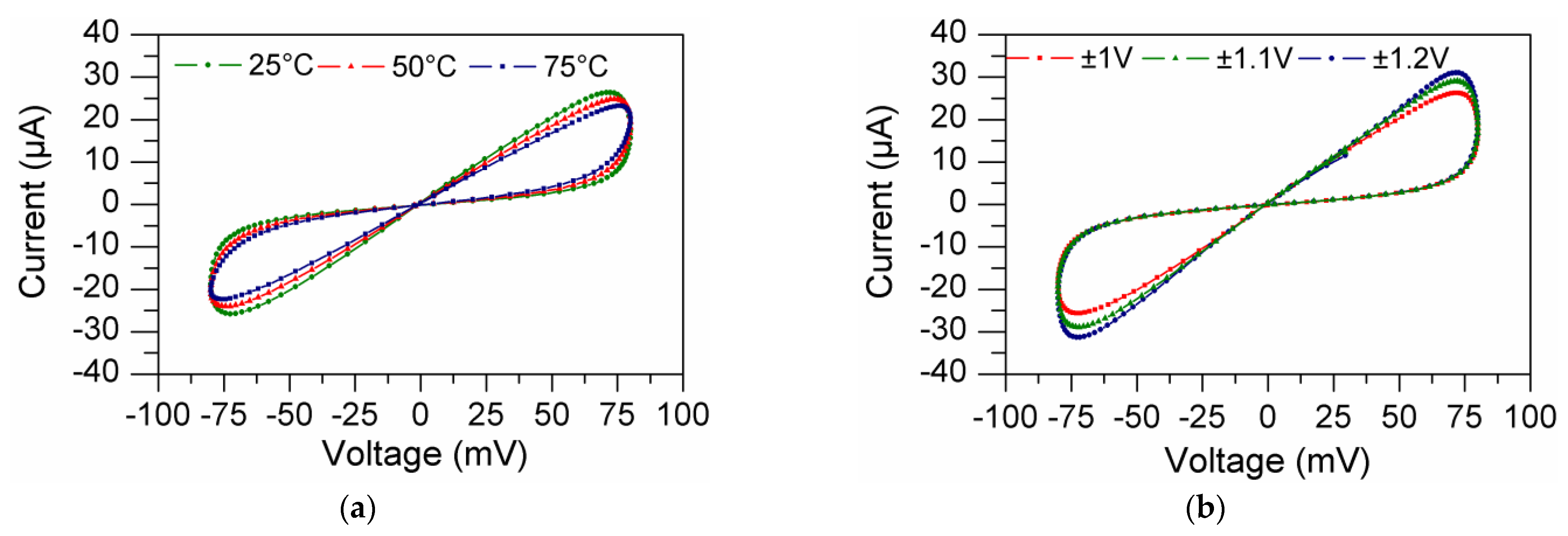
4. Non-Ideal Study of Memristor Emulator

Figure 4 illustrates the non-ideal model of the suggested memristor emulator. Both the non-idealities and parasitic of the CBTA are taken consideration in Figure 4. The voltage VB is now given as follows.
V B γ 2 g m ϕ i n C
The transconductance ( g m ) is modified as given below.
g m K ( V S S + V T H ) 1 K γ 2 ϕ i n C
The memristance is modified as given below.
M ϕ i n 1 α 1 α 2 γ 1 1 + R W Z Z 1 K V S S + V T H γ 2 ϕ i n C V S S + V T H
It is observed from (11) that the non-ideal gains and parasitic of the CBTA affect the memristance. The non-ideal gains are impactful at very high frequencies but approach unity at lower frequencies. Consequently, the impact of these non-ideal gains can be disregarded at lower frequencies. Additionally, selecting an appropriate capacitor such that C >> CZC helps minimize the effects of the parasitic.

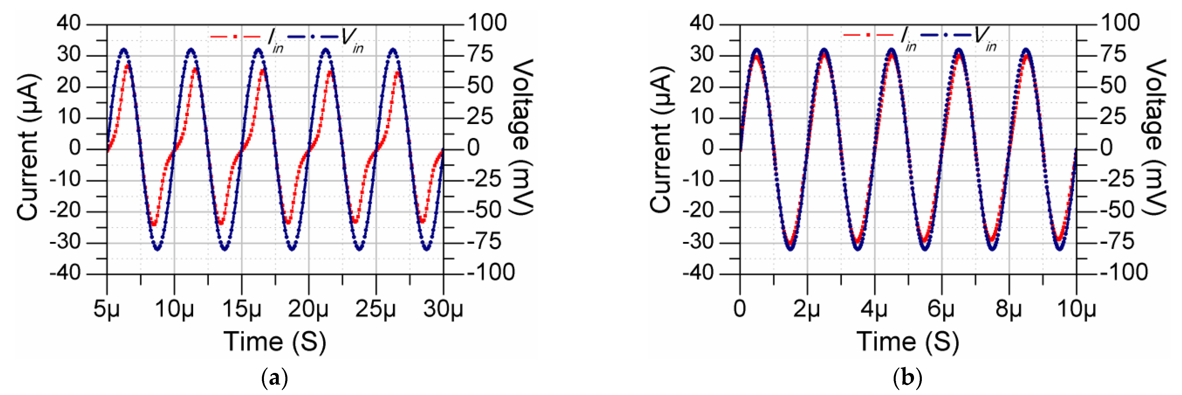
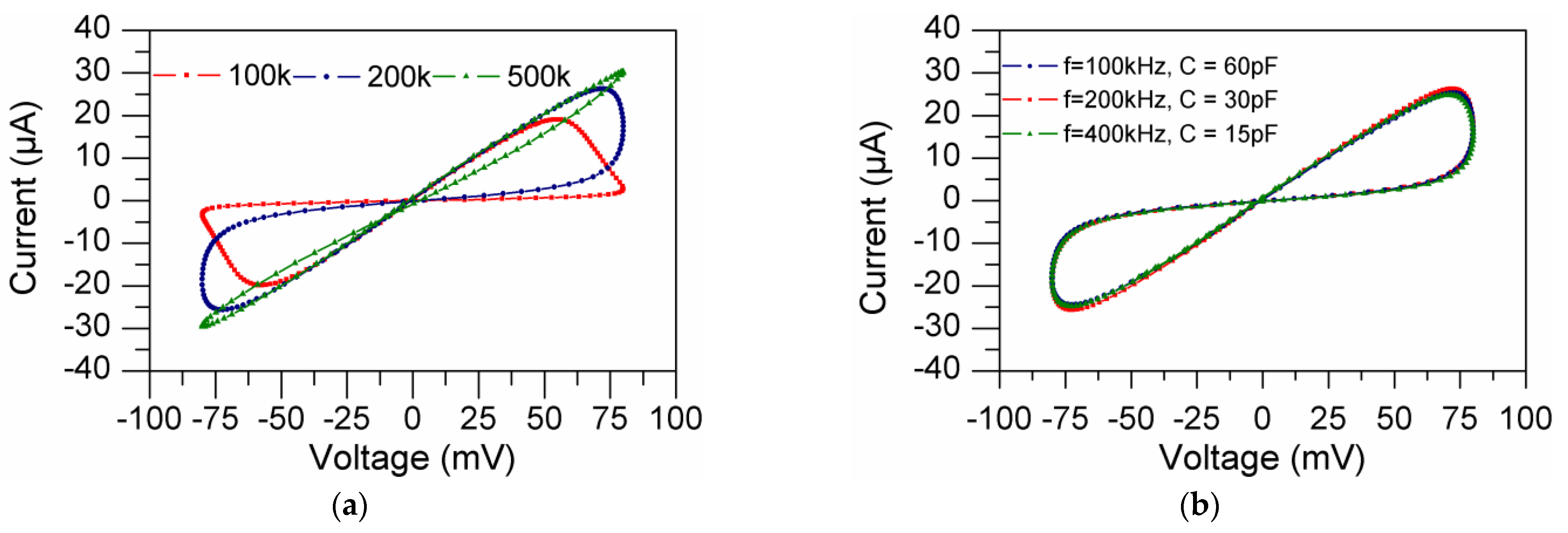
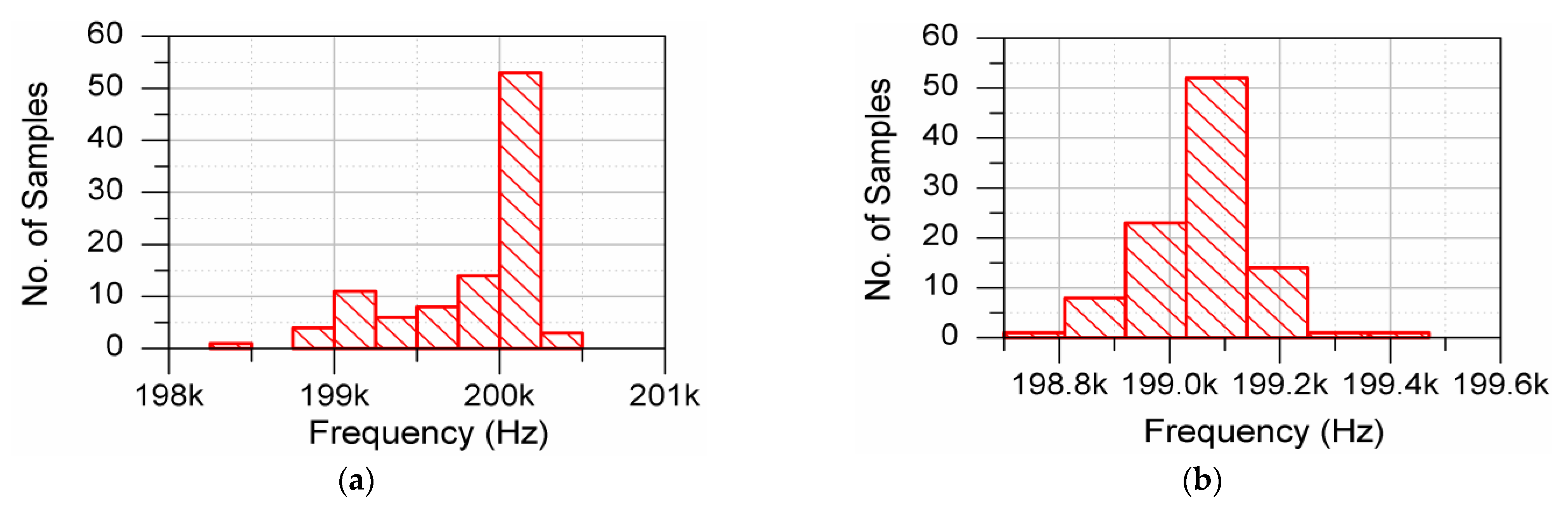
5. Simulation Results

The simulations were carried out using Cadence Virtuoso tool with 180 nm gpdk technology and ±1 V power supplies. The MOSFET’s aspect ratios are given in Table 1. Figure 5 shows the CBTA’s layout measuring 46 µm × 25.5 µm in area. To layout the CMOS structure of a CBTA, large transistors are segmented into multiple fingers. To ensure consistent matching among MOS transistors, all the transistors are positioned close together and aligned in the same direction, and the layout is kept as compact as possible. A grounded decremental ME is simulated first using C = 30 pF. The input voltage signal is applied to terminal P while terminal N is grounded. Figure 6 displays the transient responses of the suggested ME for an input voltage of 80 mV at frequencies of 200 kHz and 500 kHz. The observed current value is 32.5 μA. It is observed from Figure 6 that the non-linearity of the current signal is higher at 200 kHz frequency as compared to 500 kHz frequency. The pinch characteristics of the proposed ME at different frequencies (100, 200 and 500 kHz) are shown in Figure 7a. It is observed from Figure 7a that the non-linearity of the proposed ME decreases with the increase in frequency. Thus, the proposed ME functions as a linear resistor at higher frequencies. The pinch characteristics for constant product of frequency, f and capacitor, C are shown in Figure 7b. In Figure 7b, for different values of f and C providing the same product f × C, the pinch characteristics remain almost similar.
To check the stability of the proposed ME, its performance against the PVT variations is also examined. Monte Carlo sampling (MCS) results for MOS transistors’ mismatch and process variations are examined through 100 multiple runs using a random sampling method. Figure 8 illustrates the MCS results for the histogram of frequency of the observed current signal for MOS transistors’ mismatch and process variation when a voltage of 200 kHz frequency is applied at the input. The average value of the frequency in Figure 8a is 199.7 kHz, while in Figure 8b, it is 199 kHz. Thus, Figure 8 confirms that the proposed ME demonstrates the robust performance against mismatch and process variation. The pinch characteristics of the proposed ME against temperature and supply voltage variations are shown in Figure 9. In Figure 9a, the pinch characteristics are shown at three different temperatures, i.e., 25, 50, and 75 °C. In Figure 9b, the pinch characteristics are shown at three different supply voltages, i.e., ±1, ±1.1, and ±1.2 V. It can be seen in Figure 9 that the pinch characteristic is not adversely affected by temperature and supply voltage variations. The proposed ME is also tested at higher frequencies by selecting a capacitor with a lower value, i.e., C = 5 pF. Figure 10 shows the pinch characteristics of the proposed ME at 1, 1.5 and 2 MHz frequencies. The proposed ME works well up to 2 MHz frequency and a decrement in the non-linearity is also observed with the increase in frequency.
The time domain responses of input voltage and observed current of the suggested incremental ME for an input voltage of 80 mV at 500 kHz frequency are shown in Figure 11a. Figure 11b shows the pinch characteristics of incremental ME at different frequencies (100, 200, and 500 kHz). Figure 11b confirms that the non-linearity of the proposed incremental ME decreases with the increase in frequency. The volatile nature of the proposed incremental ME is tested by applying a voltage pulse of 80 mV with a pulse width of 200 ns and a time period of 500 ns, as depicted in Figure 12. A decrement in the amplitude of memristor current can be seen within each pulse. Thus, memristance increases in the subsequent pulses. Memristance, however, does not alter during the pulse intervals.

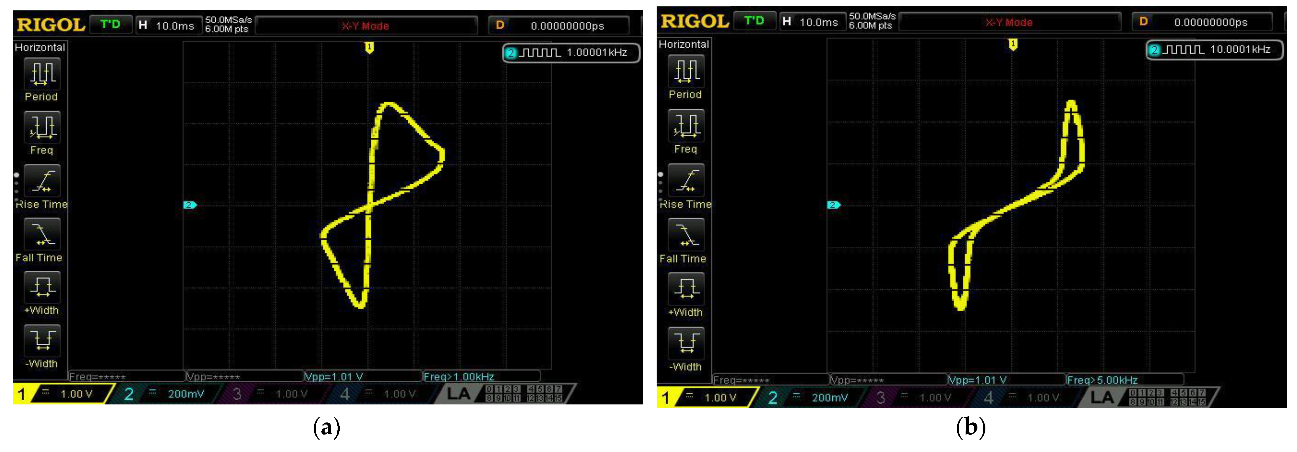
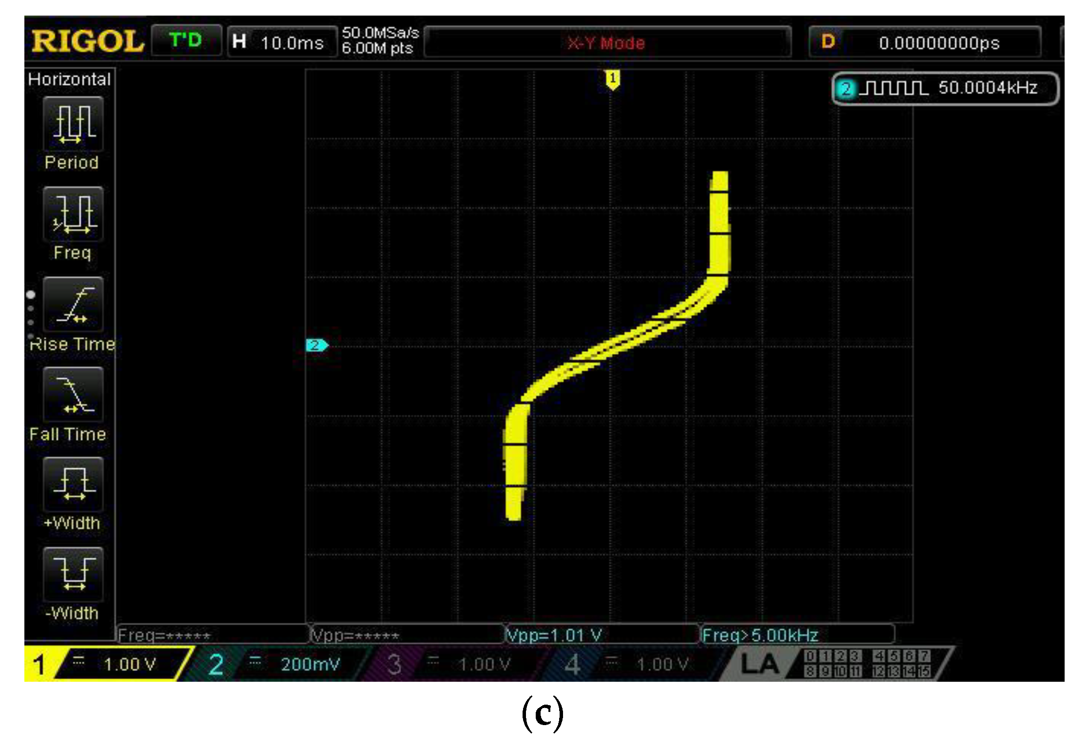
6. Experimental Verification and Comparison

The practical implementation of a CBTA which is used to realize the proposed decremental ME is shown in Figure 13. One IC for the current feedback amplifier (AD844) and two ICs for the operational transconductance amplifier (LM13700) are used to implement a prototype of CBTA. Figure 14 illustrates the experimental setup, showcasing the breadboard arrangement for mounting ICs, along with the DC power supply, function generator, and digital storage oscilloscope (DSO) used in the laboratory. The input voltage signal is generated using the RIGOL DG822 function generator and a DSO RIGOL DS1104 is used to observe the input and output waveforms. A DC power supply of ±10 V was used for the experimental results. An additional AD844 IC along with a load resistor of 1 kΩ were used to measure the memristor current, as detailed in reference [40]. A 1 V peak-to-peak amplitude sinusoidal waveform was used as an input voltage signal. The pinched characteristics of the proposed ME obtained for different frequencies (1, 10 and 50 kHz) are shown in Figure 15. The pinch characteristic is more non-linear at lower frequencies and non-linearity decreases with the increase in frequency.
A comparison between the proposed memristor emulator structure and the most pertinent previous research works [6,7,8,9,10,11,12,13,14,15,16,17,18,19,20,21,22,23,24,25,26,27,28,29,30,31,32] is given in Table 2. The ME structures reported in [22,25,28,31] are similar to the proposed ME structure as they allow for the emulation of both grounded and floating memristors in both incremental and decremental modes. The ME structures in [22,25] use two different kind of active elements and the ME in [31] uses a higher count of passive components thus these ME structures suffer from increased circuit’s complexity. The proposed ME uses the minimum number of active and passive components. Additionally, the operating frequencies of the circuits in [22,25,28,31] are less than the proposed one. Moreover, the practicality of the MEs reported in [22,25,28,31] is not examined via experimental results. It is further observed from Table 2 that the proposed emulator offers the following simultaneous features: a compact and simpler structure, the use of a minimal number of active and passive components, easy integration as it utilizes only grounded capacitor, a resistorless structure, the availability of both incremental and decremental configurations without using any additional switches, the availability of both floating and grounded type ME structures, a good operational frequency, and low operating power supplies. The proposed ME is validated using post-layout simulations and experimental results as well. These features are not simultaneously available in previous works.

7. Conclusions

In conclusion, this paper introduces a novel and compact memristor emulator structure, utilizing a single active element specifically employing a current backward transconductance amplifier and a grounded capacitor. This configuration enables the emulation of both grounded and floating memristors in both incremental and decremental configurations. The study provides a comprehensive analysis of the circuit, addressing ideal, non-ideal, and parasitic effects. The theoretical aspects are successfully validated through post-layout simulations using 180 nm gpdk technology, demonstrating the effectiveness of the proposed ME. The layout of the CBTA active block used has an area of 1.173 nm2 only. Noteworthy features include its compact structure with low voltage (±1 V) and low power consumption, making it a promising solution. The emulator exhibits robust performance against process, voltage, and temperature (PVT) variations, and it operates efficiently up to a 2 MHz frequency. Our experimental results using commercially available ICs further confirm the practicality of the solution.

Author Contributions

Conceptualization, A.K. and B.C.; methodology, A.K.; software, A.K.; validation, B.C.; formal analysis, A.K. and B.C.; investigation, A.K. and B.C.; writing—original draft preparation, A.K. and B.C.; writing—review and editing, A.K. and B.C.; supervision, B.C.; project administration, A.K. and B.C. All authors have read and agreed to the published version of the manuscript.

Funding

This work is supported by the Jaypee Institute of Information Technology, Noida, through the Directorate of Research Innovation and Development Scheme within the Organization.

Data Availability Statement

Data are contained within the article.

Conflicts of Interest

The authors declare no conflicts of interest.

References

  1. Chua, L.O. Memristor-the missing circuit element. IEEE Trans. Circuit Theory 1971, 18, 507–519. [Google Scholar] [CrossRef]
  2. Strukov, D.B.; Snider, G.S.; Stewart, D.R.; Williams, R.S. The missing memristor found. Nat. Publ. Group 2008, 453, 80–83. [Google Scholar] [CrossRef]
  3. Bao, B.; Yu, J.; Hu, F.; Liu, Z. Generalized memristor consisting of diode bridge with first order parallel RC filter. Int. J. Bifurc. Chaos 2014, 24, 1450143. [Google Scholar] [CrossRef]
  4. Corinto, F.; Ascoli, A. Memristive diode bridge with LCR filter. Electron. Lett. 2012, 48, 824–825. [Google Scholar] [CrossRef]
  5. Barboni, L. A novel passive circuit emulator for a current-controlled memristor. Act. Passiv. Electron. Compon. 2021, 2021, 5582774. [Google Scholar] [CrossRef]
  6. Yeşil, A.; Babacan, Y.; Kaçar, F. A new DDCC based memristor emulator circuit and its applications. Microelectron. J. 2014, 45, 282–287. [Google Scholar] [CrossRef]
  7. Kim, H.; Sah, M.P.; Yang, C.; Cho, S.; Chua, L.O. Memristor emulator for memristor circuit applications. IEEE Trans. Circuits Syst. I Regul. Pap. 2012, 59, 2422–2431. [Google Scholar]
  8. Yu, D.; Iu, H.H.C.; Fitch, A.L.; Liang, Y. A floating memristor emulator based relaxation oscillator. IEEE Trans. Circuits Syst. I Regul. Pap. 2014, 61, 2888–2896. [Google Scholar] [CrossRef]
  9. Sánchez-López, C.; Mendoza-Lopez, J.; Carrasco-Aguilar, M.A.; Muñiz-Montero, C. A floating analog memristor emulator circuit. IEEE Trans. Circuits Syst. II Express Briefs 2014, 61, 309–313. [Google Scholar]
  10. Abuelma’atti, M.T.; Khalifa, Z.J. A new floating memristor emulator and its application in frequency-to-voltage conversion. Analog Integr. Circuits Signal Process. 2016, 86, 141–147. [Google Scholar] [CrossRef]
  11. Raj, N.; Ranjan, R.K.; Khateb, F. Flux-controlled memristor emulator and its experimental results. IEEE Trans. Very Large Scale Integr. (VLSI) Syst. 2020, 28, 1050–1061. [Google Scholar] [CrossRef]
  12. Petrovic, P.B. Floating incremental/decremental flux-controlled memristor emulator circuit based on single VDTA. Analog Integr. Circuits Signal Process. 2018, 96, 417–433. [Google Scholar] [CrossRef]
  13. Cam, Z.G.; Sedef, H. A new floating memristance simulator circuit based on second generation current conveyor. J. Circuits Syst. Comput. 2017, 26, 1750029. [Google Scholar] [CrossRef]
  14. Yesil, A.; Babacan, Y.; Kacar, F. Electronically tunable memristor based on VDCC. AEU-Int. J. Electron. Commun. 2019, 107, 282–290. [Google Scholar] [CrossRef]
  15. Abuelma’atti, M.T.; Khalifa, Z.J. A new memristor emulator and its application in digital modulation. Analog Integr. Circuits Signal Process. 2014, 80, 577–584. [Google Scholar] [CrossRef]
  16. Sánchez-López, C.; Aguila-Cuapio, L.E. A 860 kHz grounded memristor emulator circuit. AEU-Int. J. Electron. Commun. 2017, 73, 23–33. [Google Scholar] [CrossRef]
  17. Babacan, Y.; Yesil, A.; Kacar, F. Memristor emulator with tunable characteristic and its experimental results. AEU-Int. J. Electron. Commun. 2017, 81, 99–104. [Google Scholar] [CrossRef]
  18. Umut, E.A.; Shahram, M.; Mehmet, S. Memristor emulator circuits using single CBTA. AEU-Int. J. Electron. Commun. 2017, 82, 109–118. [Google Scholar]
  19. Abuelma’atti, M.T.; Khalifa, Z.J. A continuous-level memristor emulator and its application in a multivibrator circuit. AEU-Int. J. Electron. Commun. 2015, 69, 771–775. [Google Scholar] [CrossRef]
  20. Yeşil, A.; Babacan, Y.; Kaçar, F. Design and experimental evolution of memristor with only one VDTA and one capacitor. IEEE Trans. Comput.-Aided Des. Integr. Circuits Syst. 2018, 38, 1123–1132. [Google Scholar] [CrossRef]
  21. Ranjan, R.K.; Raj, N.; Bhuwal, N.; Khateb, F. Single DVCCTA based high frequency incremental/decremental memristor emulator and its application. AEU-Int. J. Electron. Commun. 2017, 82, 177–190. [Google Scholar] [CrossRef]
  22. Yadav, N.; Rai, S.K.; Pandey, R. New grounded and floating memristor emulators using OTA and CDBA. Int. J. Circuit Theory Appl. 2020, 48, 1154–1179. [Google Scholar] [CrossRef]
  23. Cam Taskiran, Z.G.; Ayten, U.E.; Sedef, H. Dual-output operational transconductance amplifier-based electronically controllable memristance simulator circuit. Circuits Syst. Signal Process. 2019, 38, 26–40. [Google Scholar] [CrossRef]
  24. Elwakil, A.S.; Fouda, M.E.; Radwan, A.G. A simple model of double-loop hysteresis behavior in memristive elements. IEEE Trans. Circuits Syst. II Express Briefs 2013, 60, 487–491. [Google Scholar] [CrossRef]
  25. Gupta, S.; Rai, S.K. New grounded and floating decremental/incremental memristor emulator circuits based on CDTA and its application. Wirel. Pers. Commun. 2020, 113, 773–798. [Google Scholar] [CrossRef]
  26. Bhardwaj, K.; Srivastava, M. New electronically adjustable memelement emulator for realizing the behaviour of fully-floating meminductor and memristor. Microelectron. J. 2021, 114, 105126. [Google Scholar] [CrossRef]
  27. Raj, A.; Singh, S.; Kumar, P. Dual mode, high frequency and power efficient grounded memristor based on OTA and DVCC. Analog Integr. Circuits Signal Process. 2022, 110, 81–89. [Google Scholar] [CrossRef]
  28. Yadav, N.; Rai, S.K.; Pandey, R. Novel memristor emulators using fully balanced VDBA and grounded capacitor. Iran. J. Sci. Technol. Trans. Electr. Eng. 2021, 45, 229–245. [Google Scholar] [CrossRef]
  29. Sharma, P.K.; Prasad, S.S.; Tasneem, S.; Priyadarshini, B.; Ranjan, R.K. Resistive tunable memristor emulator model and its application. AEU-Int. J. Electron. Commun. 2023, 160, 154500. [Google Scholar] [CrossRef]
  30. Bhardwaj, K.; Srivastava, M. Compact floating dual memelement emulator employing VDIBA and OTA: A novel realization. Circuits Syst. Signal Process. 2022, 41, 5933–5967. [Google Scholar] [CrossRef]
  31. Suresha, B.; Shankar, C.; Rudraswamy, S.B. A floating memristor emulator for analog and digital applications with experimental results. Analog Integr. Circuits Signal Process. 2024, 118, 77–90. [Google Scholar] [CrossRef]
  32. Bhardwaj, K.; Srivastava, M. New multiplier-less compact tunable charge-controlled memelement emulator using grounded passive elements. Circuits Syst. Signal Process. 2022, 41, 2429–2465. [Google Scholar] [CrossRef]
  33. Romero, F.J.; Ohata, A.; Toral-Lopez, A.; Godoy, A.; Morales, D.P.; Rodriguez, N. Memcapacitor and meminductor circuit emulators: A review. Electronics 2021, 10, 1225. [Google Scholar] [CrossRef]
  34. Petrović, P.B. Electronically adjustable grounded memcapacitor emulator based on single active component with variable switching mechanism. Electronics 2022, 11, 161. [Google Scholar] [CrossRef]
  35. Romero, F.J.; Escudero, M.; Medina-Garcia, A.; Morales, D.P.; Rodriguez, N. Meminductor emulator based on a modified Antoniou’s gyrator circuit. Electronics 2020, 9, 1407. [Google Scholar] [CrossRef]
  36. Yesil, A.; Babacan, Y.; Kacar, F. A new floating memristor based on CBTA with grounded capacitors. J. Circuits Syst. Comput. 2019, 28, 1950217. [Google Scholar] [CrossRef]
  37. Kumar, A.; Chaturvedi, B.; Jagga, S. New CMOS compatible realizations of grounded/floating L, C multiplier and FDNC simulators. Circuits Syst. Signal Process. 2023, 42, 1911–1939. [Google Scholar] [CrossRef]
  38. Chaturvedi, B.; Kumar, A. A novel electronically controlled Schmitt trigger with clockwise and anticlockwise hystereses. AEU-Int. J. Electron. Commun. 2018, 89, 136–145. [Google Scholar] [CrossRef]
  39. Chaturvedi, B.; Kumar, A. High CMRR current-mode instrumentation amplifier for low voltage and low power applications. AEU-Int. J. Electron. Commun. 2019, 104, 147–154. [Google Scholar] [CrossRef]
  40. Kumar, A.; Chaturvedi, B.; Mohan, J. Minimal realizations of integrable memristor emulators. J. Comput. Electron. 2023, 22, 504–518. [Google Scholar] [CrossRef]
Figure 1. (a) CBTA symbol; (b) CMOS implementation of CBTA [36].
Electronics 13 03331 g001
Figure 2. Parasitic model of CBTA.
Electronics 13 03331 g002
Figure 3. Proposed decremental/incremental memristor emulator.
Electronics 13 03331 g003
Figure 4. Non-ideal model of the proposed memristor emulator.
Electronics 13 03331 g004
Figure 5. Layout of CBTA.
Electronics 13 03331 g005
Figure 6. Transient responses for input voltage and current at (a) 200 kHz and (b) 500 kHz.
Electronics 13 03331 g006
Figure 7. Pinch characteristics of the proposed decremental memristor (a) at different frequencies and (b) for a constant product of f and C.
Electronics 13 03331 g007
Figure 8. MCS results for frequency variations of input current signal for (a) MOS transistors’ mismatch and (b) the process variation.
Electronics 13 03331 g008
Figure 9. Pinch characteristics at different (a) temperatures and (b) supply voltages.
Electronics 13 03331 g009
Figure 10. Pinch characteristics at different higher frequencies for C = 5 pF.
Electronics 13 03331 g010
Figure 11. Simulation results of incremental memristor (a) transient responses for input voltage and current at 500 kHz. (b) Pinch characteristics at different frequencies.
Electronics 13 03331 g011
Figure 12. Transient responses for input voltage and current which confirm the volatility.
Electronics 13 03331 g012
Figure 13. Experimental realization of CBTA used to realize the grounded ME.
Electronics 13 03331 g013
Figure 14. Experimental setup.
Electronics 13 03331 g014
Figure 15. Pinch characteristics at different temperatures: (a) 1 kHz, (b) 10 kHz, (c) 50 kHz.
Electronics 13 03331 g015aElectronics 13 03331 g015b
Table 1. Aspect ratios of MOS transistors.
MOSFETW/L
M1–M3, M17–M194.5 µm/0.36 µm
M4, M522.5 µm/0.36 µm
M6, M75 µm/0.36 µm
M8, M915 µm/0.36 µm
M10, M117.5 µm/0.36 µm
M12–M14, M20–M221.5 µm/0.36 µm
M15, M1630 µm/0.18 µm
M23–M273.6 µm/1.8 µm
M28, M29, M327.2 µm/1.8 µm
M30, M31,M332.4 µm/1.8 µm
Table 2. A comparison between the proposed ME and the most pertinent previous research.
Ref.Count of Active ComponentsPassive Components/CountAll Grounded Passive ComponentsIncremental/DecrementalFloating (F)/Grounded (G) StructureSupply Voltages (V)Operational FrequencySim/Exp
Results
61 DDCC, 1 MultiplierR/2, C/1NoBothF±1.51 MHzSim
75 OPAMP, 1 Multiplier, 10 MOSFETR/8, C/1NoBothF±5800 HzBoth
84 AD844, 1 AD633, 1 OPAMPR/8, C/1NoDecrementalF±15120 HzExp
94 AD844, 1 AD633 R/5, C/1NoBothF±1020.2 kHzBoth
104 CFOA, 2 DR/4, C/4NoIncrementalFNA6 kHzExp
11 1 CCII, 1 OTA R/1, C/1YesBothG±1.226.3 MHzBoth
121 VDTA, 1 MultiplierR/2, C/1YesBothF±0.92 MHzBoth
134 CCII, 1 MultiplierR/3, C/1NoBothF±1040 kHzBoth
141 VDCC, 2 MOSFETC/1YesBothG±0.92 MHzBoth
153 CFOA (AD844), 1 DR/4, C/2NoBothGNA700 HzExp
161 AD844, 1 Multiplier (AD633) R/1, C/1NoBothG±10860 kHzBoth
171 MO-OTA, 1 MultiplierR/1, C/1YesBothG±1.25 5 kHzBoth
181 CBTA,1 MultiplierR/2, C/1NoBothG±0.9460 kHzSim
192 CFOA, 1 OTAR/3, C/2YesDecrementalG±12600 HzExp
201 VDTAMOS-C/1YesBothG±0.950 MHzBoth
211 DVCCTAR/3, C/1NoBothG±1.251 MHzSim
221 CDBA, 1 OTAC/1YesBothBoth±0.91 MHzSim
232 OTA, 1 MultiplierR/1, C/1YesBothF±1.5180 kHzBoth
242 CCII, 1 Multiplier, 1 BufferR/3, C/1NoBothG±10100 kHzBoth
251 CDTA, 1 OTAC/1YesBothBoth±0.92 MHzSim
262 VDTAR/1, C/1YesBothF±0.91.5 MHzSim
271 OTA, 1 DVCCR/1, C/1YesBothG±1.21 MHzSim
281 FB-VDBAC/1YesBothBoth±0.91 MHzSim
291 DVCC, 1 OTAR/1, C/1YesBothG±0.930 MHzBoth
301 VDIBA, 1 OTA, 2 MOSR/1, C/1YesBothF±18 MHzBoth
311 OPAMP, 1 MOSFETR/5, C/1NoBothBoth±1.520 kHzBoth
321 VDCC, 1 OTAR/2, C/1YesIncrementalG---1 MHzBoth
This work1 CBTAC/1YesBothBoth±12 MHzBoth
Abbreviations: DDCC: differential difference current conveyor; OPAMP: operational amplifier; CCII: second-generation current conveyor; CFOA: current feedback operational amplifier; OTA: operational transconductance amplifier; VDTA: voltage differencing transconductance amplifier; VDCC: voltage differencing current conveyor; MO-OTA: multi-output operational transconductance amplifier; CBTA: current backward transconductance amplifier; DVCCTA: differential voltage current conveyor transconductance amplifier; CDBA: current differencing buffered amplifier; CDTA: current differencing transconductance amplifier; DVCC: differential voltage current conveyor; VDIBA: voltage differencing inverted buffered amplifier C: capacitor; R: resistor; D: diode; NA: not available; Sim: simulation; Exp: experimental.
Disclaimer/Publisher’s Note: The statements, opinions and data contained in all publications are solely those of the individual author(s) and contributor(s) and not of MDPI and/or the editor(s). MDPI and/or the editor(s) disclaim responsibility for any injury to people or property resulting from any ideas, methods, instructions or products referred to in the content.

