Article

A Dual Constant Current Output Ports WPT System Based on Integrated Coil Decoupling: Analysis, Design, and Verification

1
College of Electronics and Electrical Engineering, Harbin University of Science and Technology, Harbin 150080, China
2
College of Electronic and Electrical Engineering, Henan Normal University, Xinxiang 453007, China
3
College of Intelligent Manufacturing, Hunan University of Science and Engineering, Yongzhou 425199, China
*
Author to whom correspondence should be addressed.
Electronics 2024, 13(17), 3371; https://doi.org/10.3390/electronics13173371
Submission received: 26 July 2024 / Revised: 21 August 2024 / Accepted: 23 August 2024 / Published: 25 August 2024
(This article belongs to the Special Issue New Insights in Power Electronics: Prospects and Challenges)

Abstract

:
With the high integration of power electronic devices, wireless power transfer (WPT) systems are required to have output characteristics of different specifications that are independent of the load. However, existing methods for realizing dual-output WPT systems have problems such as complex circuits, cumbersome control schemes, low system stability, insufficient system space utilization, and unnecessary cross-coupling. Therefore, in order to solve the above problems, this paper proposes a dual-receiver WPT system with dual constant current (CC) output based on an integrated decoupling coil. In this system, the DD coil is wound vertically in series with the solenoid coil and serves as the first receiving coil to achieve energy transmission in the system. While the solenoid coil is used in the transmitting coil and the second receiving coil, and the coils are perpendicular to each other to achieve natural decoupling. Furthermore, the receiving coils are integrated together on the receiving side ferrite plate. Therefore, there is no cross-coupling interference in the system, which simplifies the system design. Firstly, the natural decoupling characteristics of the magnetic coupler and the coil optimization method are analyzed in detail theoretically. Secondly, a detailed mathematical analysis is performed on the dual CC output characteristics with different specifications that are load-independent and have zero phase angle operation. Again, the zero voltage switching of the inverter can be achieved by changing the compensation component parameters through simulation verification. Finally, a prototype with a rated power of 283 W is constructed for validation purposes. The first receiver delivers a CC output of 3 A, while the second receiver provides a CC output of 4 A, with the DC–DC conversion efficiency reaching a peak of 90.2%. The experimental results confirm the accuracy of the theoretical analysis.

1. Introduction

Wireless power transmission (WPT) has been widely used in many fields for its safety, reliability, and convenience [1,2], such as in consumer electronics [3], electric vehicles (EVs) [4], and other industrial fields [5,6]. Compared with traditional single-channel WPT systems, its advantages can be further demonstrated in systems using multiple receivers [7,8].
With the high integration of power electronic devices, WPT systems need to achieve multiple CC outputs simultaneously, such as powering multiple OLED panels [9,10] and multi-output chargers for electric vehicles [11]. Generally, WPT systems follow a dual-coil structure, which uses a transmitter and a receiver to transmit power [12,13]. As dual output currents need to be generated, DC–DC converters [14,15,16] and dual resonant circuits [17] are mainly used. In the literature [14,15,16], it has been difficult to achieve a wide range of parameter conversions using DC–DC converters. In order to solve this problem, additional circuits and control methods have been used in the literature [16] to increase the parameter adjustment range, but the additional circuits and complex controls will undoubtedly increase the hardware cost of the system, the weight of the equipment, and the power loss of the system. The method using dual resonant converters in [17] also suffers from the same problem, because this method requires additional passive components to generate dual output currents.
In order to overcome the above shortcomings, different outputs can be achieved by configuring the mutual inductance between each transmitter and receiver of the dual-channel system [18,19]. However, the use of a multi-emitter structure will greatly limit the installation space of the system. Therefore, this is not applicable to some equipment with limited installation space [20]. Furthermore, the purpose of a compact system structure can be achieved by reasonably configuring the parameters of the three-coil WPT system [21]. But, for systems using dual receivers, cross-coupling always exists, affecting the transmission efficiency and independent output of the system [22]. Therefore, specific methods are required to eliminate the interference caused by cross-coupling.
In current research, decoupling methods can be broadly categorized into three types: using additional decoupling reactors, employing magnetic shielding, and designing with magnetic couplers. The method involving decoupling reactors [23] requires supplementary compensation capacitors to eliminate unnecessary cross-coupling, which necessitates additional installation space and restricts the circuit’s freedom. To address the practical needs and enhance the system flexibility, researchers [24,25] have introduced additional frequency control circuits to dynamically adjust the resonant frequency, thereby mitigating the effects of cross-coupling. However, this approach can lead to frequency bifurcation, posing significant challenges to the stability of WPT systems.
Additionally, the use of magnetic shielding necessitates a composite structure comprising relay coils and ferrite plates to sequentially transmit energy, thereby mitigating the impact of cross-coupling [25,26]. However, the bifurcation phenomenon associated with this method poses significant challenges to the stability of the WPT system. Therefore, the design of magnetic couplers has been widely studied, as their magnetic cancellation principle can mitigate the influence of different coils [27,28,29]. In [27,28], a double D quadrature (DDQ) coil structure and a double D coil structure were used to eliminate cross-coupling, respectively. However, they require precise placement, and when there is misalignment in the horizontal direction, the magnetic decoupling characteristics of the magnetic coupler fail. Therefore, the flexibility of the magnetic coupler design is greatly limited. Furthermore, in [29], for the bipolar (BP) structure, as the two coils only partially overlap, it results in low space utilization.
In order to solve the shortcomings of the above-mentioned traditional dual-output WPT system, such as the complex circuits and control methods adopted in [14,15,16,17], the influence of unnecessary cross−coupling in [18,19,22], the insufficient system stability in [24,25], the low space utilization of the dielectric system in [26,27,28,29,30], and the failure of the decoupling characteristics when the magnetic coupler is offset in [28,29], a dual CC output WPT system is proposed in this paper. The DD coil is wound vertically in series with the solenoid coil, serving as the first receiving coil in the system to achieve energy transfer; meanwhile, the solenoid coil is used for the transmitting coil and the second receiving coil, and the two coils are perpendicular to each other to achieve natural decoupling. The transmitter side adopts an S compensation structure, the first receiving side adopts an S compensation structure, and the second receiving side adopts an LCC compensation structure. Furthermore, the special magnetic coupler design and coil optimization method improve the space utilization of the system. Therefore, the system can obtain two load-independent CC outputs and ZPA characteristics with fewer compensation components, and ensure the compactness of the system. In addition, the ZVS operation of the system can be achieved by fine-tuning compensation components. This method can reduce the informal loss of the system and further improve the efficiency of the system.
The remainder of this paper is structured as follows. Section 2 introduces the proposed magnetic coupler and its optimization methodology. Then, a detailed mathematical analysis of the proposed WPT system is carried out in Section 3. Section 4 validates the frequency characteristics of the dual CC output WPT system under ZPA conditions through simulations and discusses the implementation of ZVS operation. In Section 5, a verification experimental prototype with a rated power of 283 W is manufactured, demonstrating the system’s practicality with output currents of 4 A and 3 A for the first and second receivers, respectively. Finally, the conclusions are summarized in Section 6.

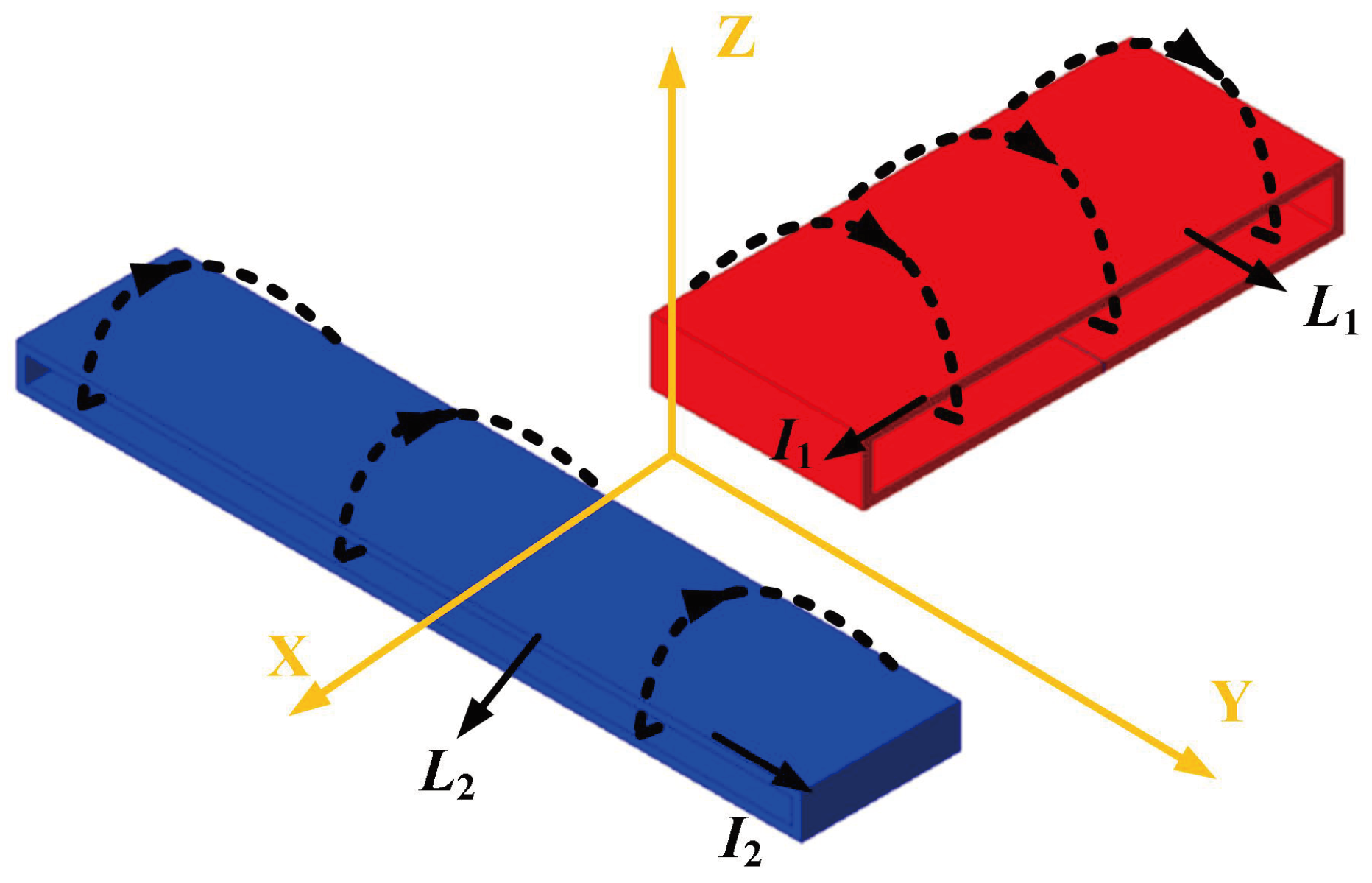
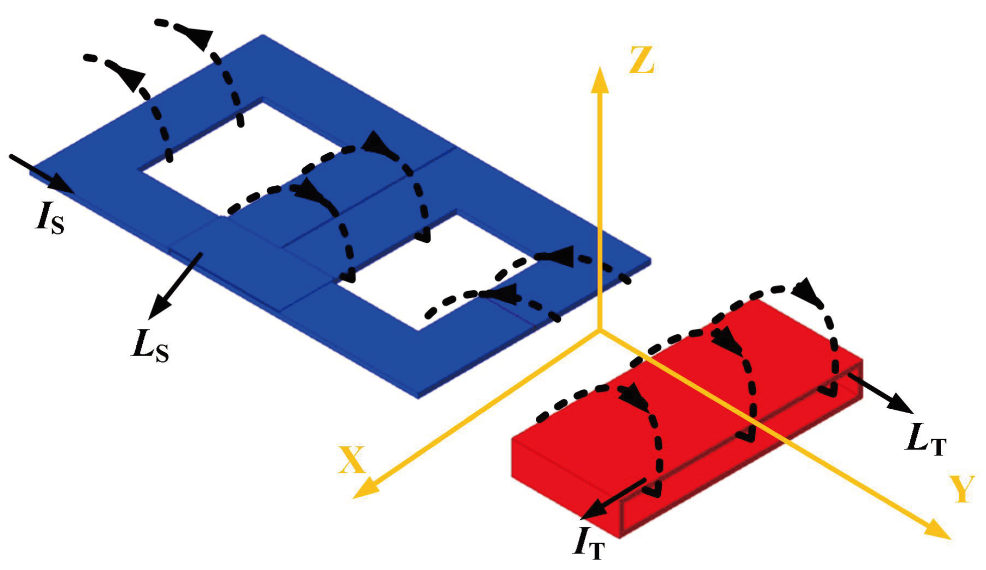
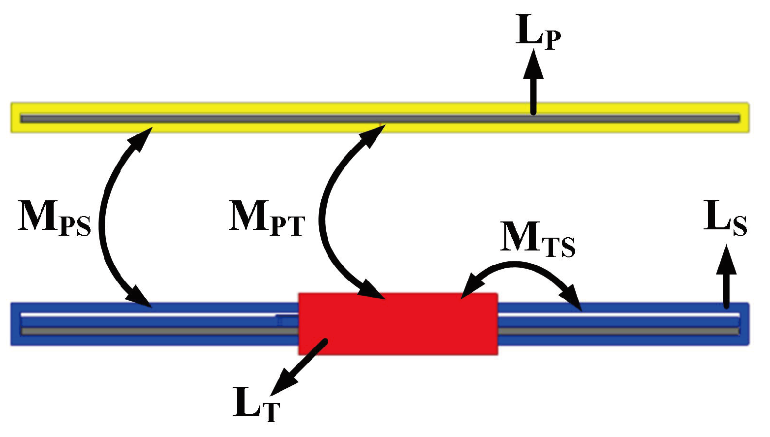
2. Theoretical Analysis of Transmitter Side Decoupling Coil Magnetic Coupler

Given that dual receivers play a key role in the proposed WPT system with step-by-step energy transmission, a dedicated decoupling design is required. That is, the mutual inductance between the system’s transmitting coil and the second receiving coil needs to be designed to be zero. Figure 1 shows the magnetic flux distribution between two solenoid coils that are perpendicular to each other. It is obvious that the magnetic fields of the two solenoid coils radiate from their centers, and the magnetic field directions are perpendicular to each other. The red solenoid coil produces magnetic flux that is parallel to the Y−Z plane, while the blue solenoid coil produces magnetic flux that is parallel to the X−Z plane. Therefore, the magnetic flux from the red solenoid coil does not flow into the blue solenoid coil, and similarly, the magnetic flux from the blue solenoid coil does not flow into the red solenoid coil. To examine the coupling between the two perpendicular solenoid coils, they are denoted as L 1 and L 2 , respectively. In this context, the magnetic flux ψ 21 primarily refers to the flux generated by the current in coil L 2 that passes through coil L 1 . Here, B 2 denotes the magnetic induction of coil L 2 , while S 1 represents the area of coil L 1 . Therefore, the magnetic flux between the two solenoid coils ψ 21 can be expressed as follows:
ψ 21 = B 2 · d S 1
It can be readily concluded that the magnetic flux produced by the blue solenoid coil L 2 does not intersect with the red solenoid coil L 1 . Consequently, ψ 21 is zero. The mutual inductance M 12 between the two solenoid coils is excited by the current I 2 flowing through L 2 and is expressed as follows:
M 12 = ψ 21 I 2
Equations (1) and (2) show that M 12 is zero, indicating that the two solenoid coils, oriented perpendicularly to each other, are magnetically decoupled.
For the WPT system with dual receivers proposed in this paper, as the first receiving coil also acts as a relay coil, it needs to receive the energy from the transmitting side and transfer it to the second receiving coil for reception. Therefore, the first receiving coil is formed by connecting a DD coil and a solenoid coil in series, the transmitting coil and the second receiving coil are both formed by a solenoid coil, and the second receiving coil and the transmitting coil are both perpendicular to the solenoid coil in the first receiver. For the design requirements of the traditional three-coil system, there needs to be a certain air gap distance between the three coils. However, for some systems that are limited by installation space, it is difficult to achieve the installation requirements of traditional three-coil equipment. Therefore, the coil structure needs to be optimized. The first receiver coil and the second receiver coil are integrated together on the receiving side ferrite board, which optimizes the air gap distance in the coherent arrangement mode, can meet the installation requirements of the system realizing dual-channel output in a small space and achieve better coupling effect. Figure 2 shows the magnetic flux distribution of the DD-type coil in both the first and second receiving coils. It can be clearly seen that the magnetic flux generated by the DD coil and the solenoid coil flows through each other. That is, the mutual inductance between the first receiving coil and the second receiving coil is not zero. Therefore, the first receiving coil and the second receiving coil can be integrated on the receiving-side ferrite plate. Combined with the above analysis, the structural diagram and optimization scheme of the magnetic coupler are shown in Figure 3. Compared with the traditional three-coil structure, the space utilization of the system is increased. The magnetic coupling schematic diagram of the magnetic coupler is shown in Figure 4. L P represents the transmitting coil. L T and L S represent the first receiving coil and the second receiving coil, respectively. M P T , M T S , and M P S represent the mutual inductance between L P and L T , L T and L S , L P and L S . It is worth emphasizing that the magnetic flux directions between L P and L S are always perpendicular to each other when no rotational offset occurs, so no matter if horizontal or vertical dislocation occurs, the mutual inductance M P S is always approximately zero, that is, the magnetic decoupling characteristics of the proposed magnetic coupler are not affected by the influence of the situation.

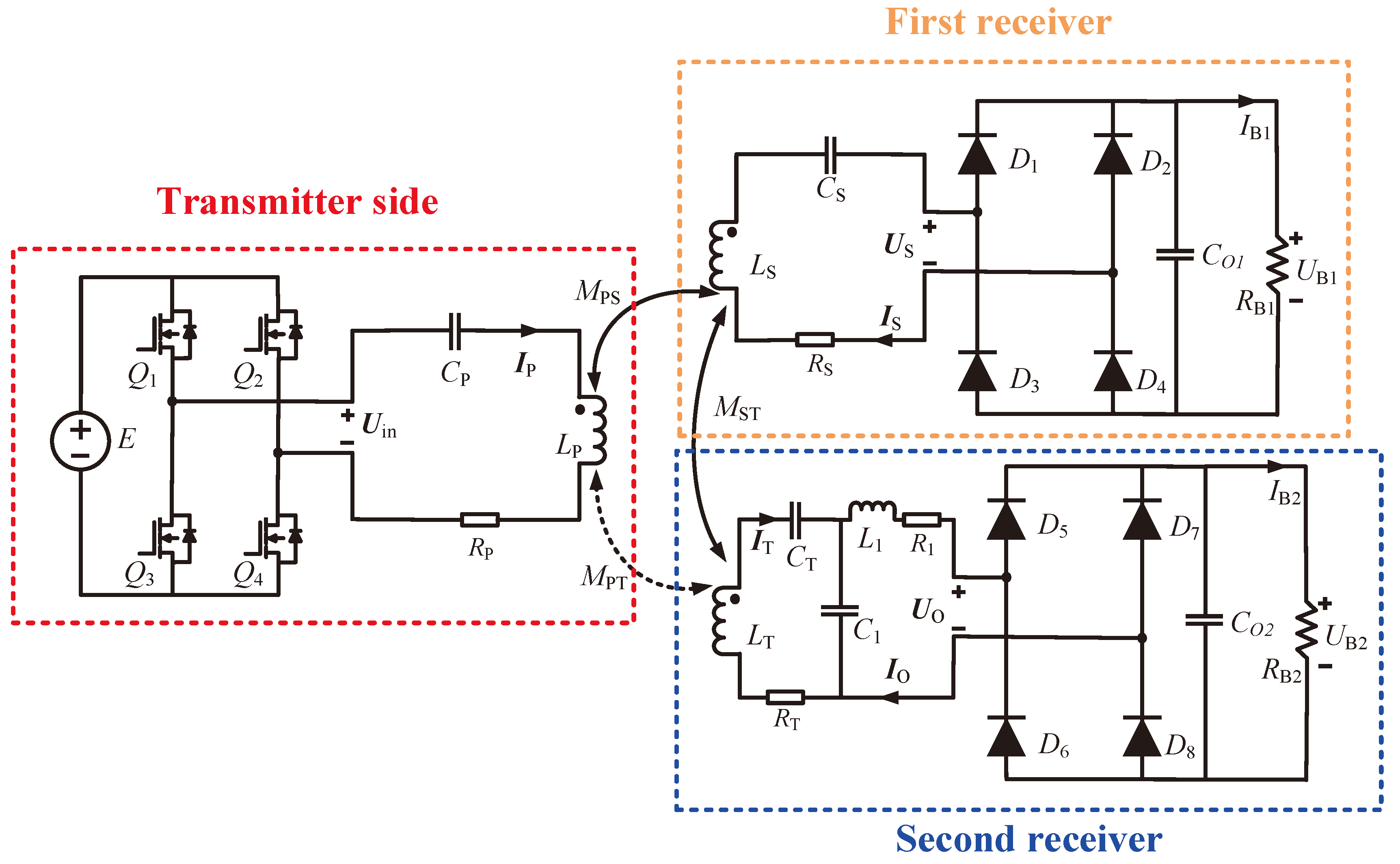
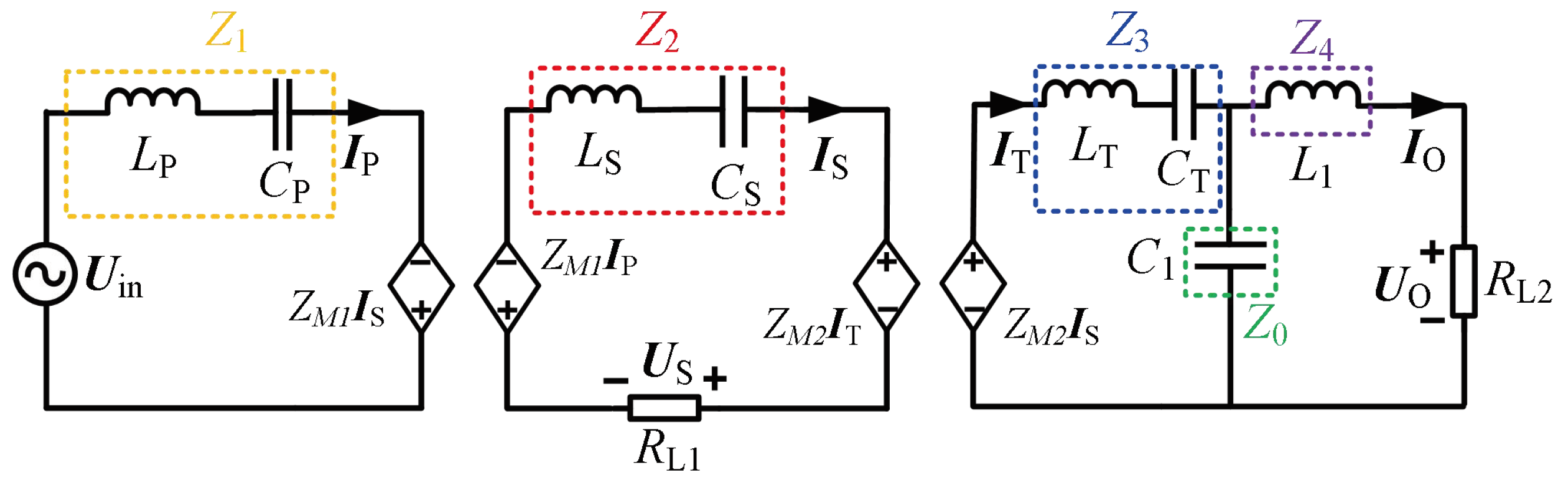
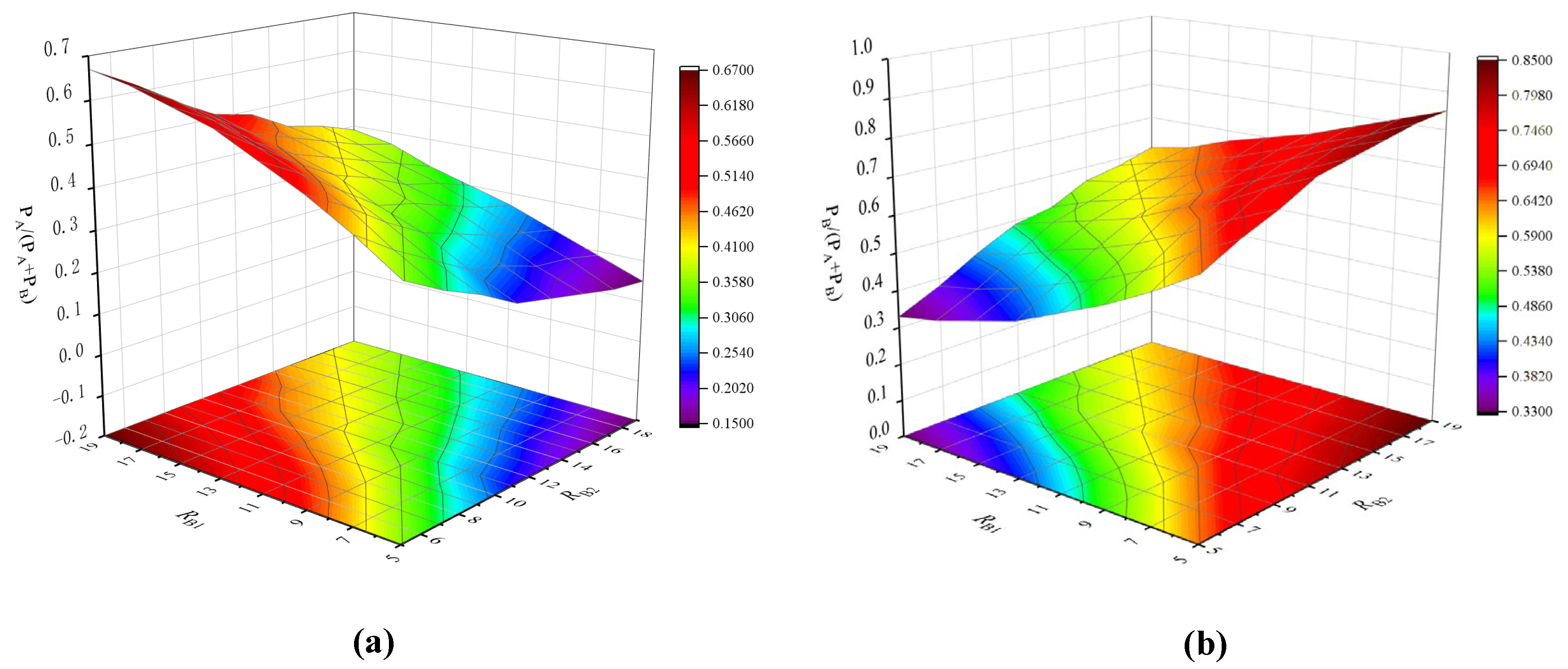
3. Theoretical Analysis

Because of its own structural characteristics, the S−S−LCC compensation topology can meet the output characteristics of the dual output WPT system. Therefore, this paper selects the S−S−LCC compensation structure as the topology for subsequent research. The overall circuit architecture of the proposed dual CC output WPT system based on integrated decoupling coils is shown in Figure 5. E is the DC input voltage source of the system. The high-frequency inverter (HFI) consists of four MOSFETs ( Q 1 Q 4 ). L P is the self-inductance of the transmitting coil, L S is the self-inductance of the first receiving coil, L T is the self-inductance of the second receiving coil, and L 1 is the compensation inductance of the second receiver. C P , C S , C T , and C 1 are the compensation capacitors of the circuit, respectively, and R P , R S , R T , and R 1 are the parasitic internal resistances of each coil, respectively, C O 1 and C O 2 are the filter capacitors of the receivers, and R B 1 and R B 2 are the equivalent resistances of the two receiver loads. M P S , M S T , and M P T represent the mutual inductance between the three coils. As the proposed system needs to utilize the mutual inductance between receivers to transfer energy, that is, the energy is first transferred from the transmitting coil to the first receiving coil and then to the second receiving coil. Therefore, in order to meet the requirements of energy transfer. Because of the proposed decoupling mechanism, the unwanted cross-coupling ( M P T ) can be eliminated. Therefore, only two main mutual inductances need to be considered, namely M P S and M S T . U i n is the AC output voltage of HFI. The fundamental wave analysis method is used to obtain the RMS form of the output voltage fundamental component of the inverter:
U i n = 2 2 π E 0
I P , I S , I T , and I O are the current phasors flowing through each current loop. The two receivers are connected correspondingly by full-bridge rectifiers composed of diodes ( D 1 D 4 ) and ( D 5 D 8 ), in order to convert the AC current I S , I O into a DC charging current to I B 1 , I B 2 to power the receiver load. The mathematical relationship between the two rectifier input current phasors I S , I O and the DC charging currents I B 1 , I B 2 is as follows:
I S = 2 2 π I B 1 I O = 2 2 π I B 2
In order to facilitate the subsequent analysis, the parasitic internal resistance in each coil is ignored, and the equivalent circuit diagram of the proposed dual-output WPT system is shown in Figure 6. Among them, R L 1 and R L 2 are the AC equivalent resistances of the load equivalent circuits R B 1 and R B 2 , respectively. Similarly, their mathematical relationship expressions are as follows:
R L 1 = 8 π 2 R B 1 R L 2 = 8 π 2 R B 2
To simplify the calculation, the parameters of the circuit are given as follows:
Z 0 = 1 j ω C 1 Z 1 = 1 j ω C P + j ω L P Z 2 = 1 j ω C S + j ω L S Z 3 = 1 j ω C T + j ω L T Z 4 = j ω L 1 Z M 1 = j ω M P S Z M 2 = j ω M S T
According to the resonance principle of the circuit, the following equation needs to be satisfied:
Z 1 = 0 Z 2 = 0 Z 0 + Z 3 = 0 Z 0 + Z 4 = 0
According to Kirchhoff’s voltage law (KVL), the voltage relationship of each circuit in the proposed dual-output WPT system is expressed as follows:
U i n = Z 1 I P Z M 1 I S 0 = Z M 1 I P + Z 2 + R L 1 I S + Z M 2 I T 0 = Z M 2 I S + Z 3 + Z 0 I T Z 0 I O 0 = Z 0 I T + Z 4 + Z 0 + R L 2 I O
Under the conditions of (7), the output current I S of the first receiver and the output current I O of the second receiver can be obtained from (8) as follows:
I S = j U i n ω M P S I O = j ω C 1 M S T M P S U i n
In addition, the input impedance of the dual-output WPT system is defined as Z i n = U i n / I P . From (8), the input impedance Z i n of the system is:
Z i n = R L 1 ω M P S 2 ω C 1 M S T M P S 2 R L 2
From (9) and (10), it can be seen that Z i n is purely resistive, that is, the system can achieve two CC outputs that are independent of the load under the condition of ZPA.

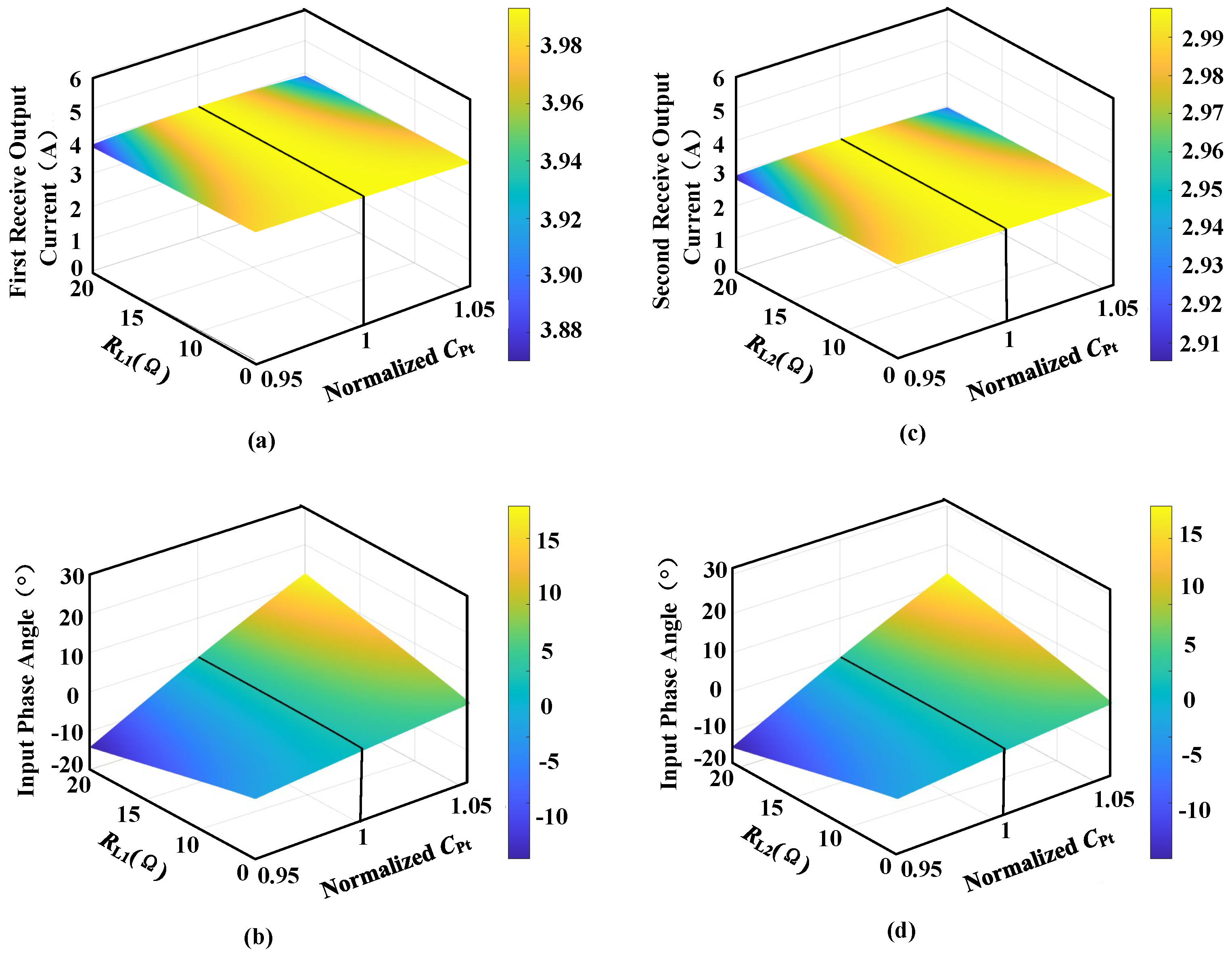
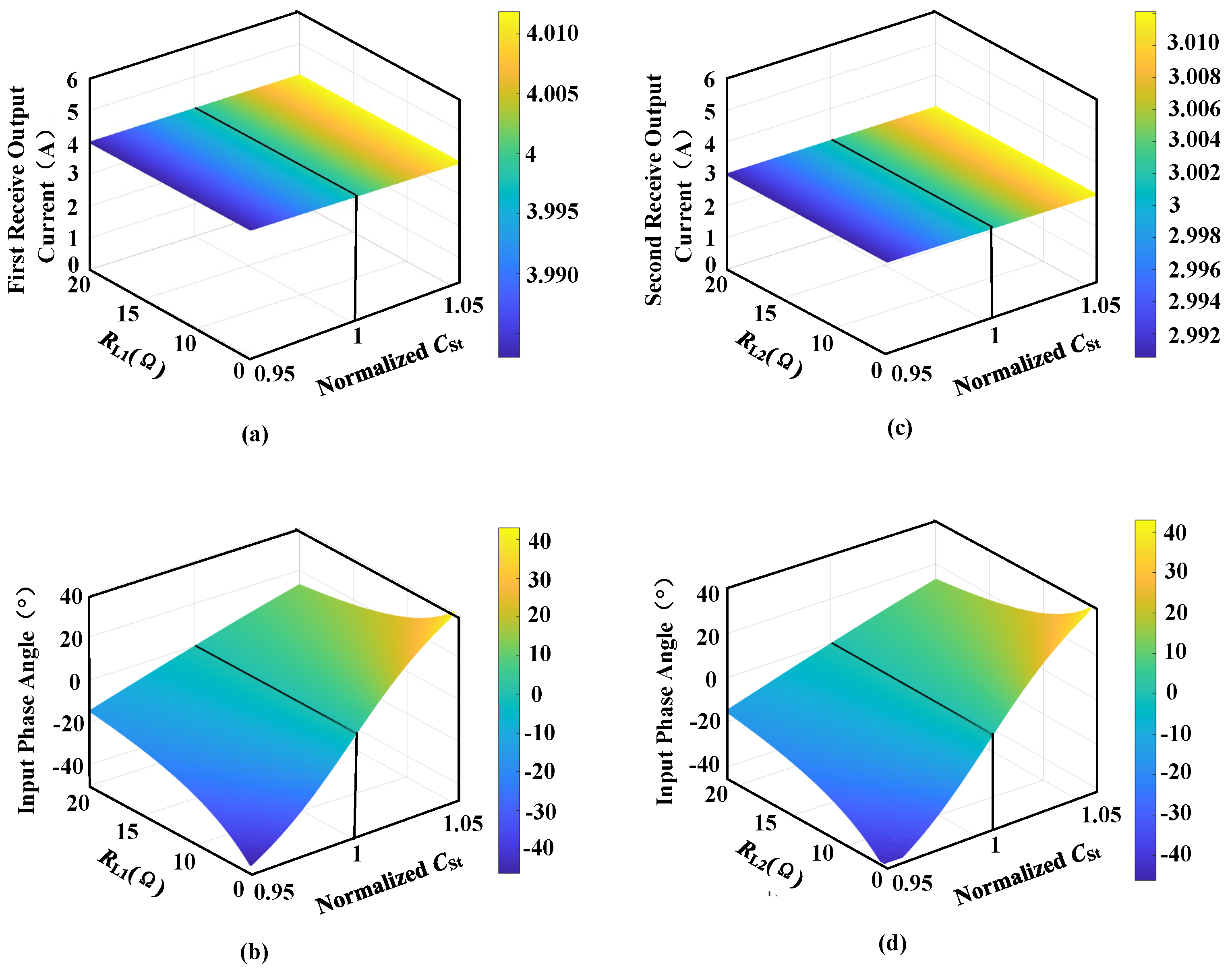
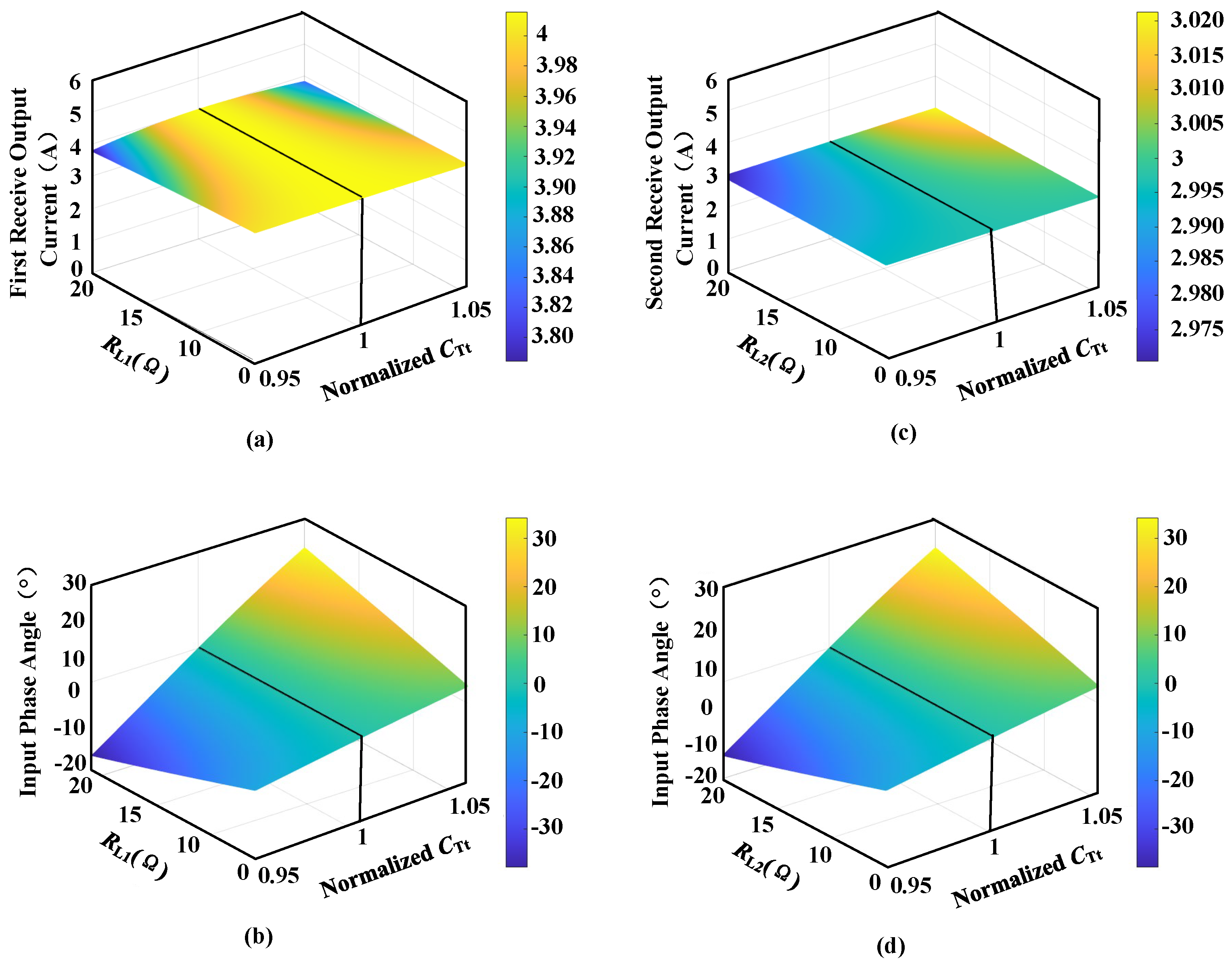
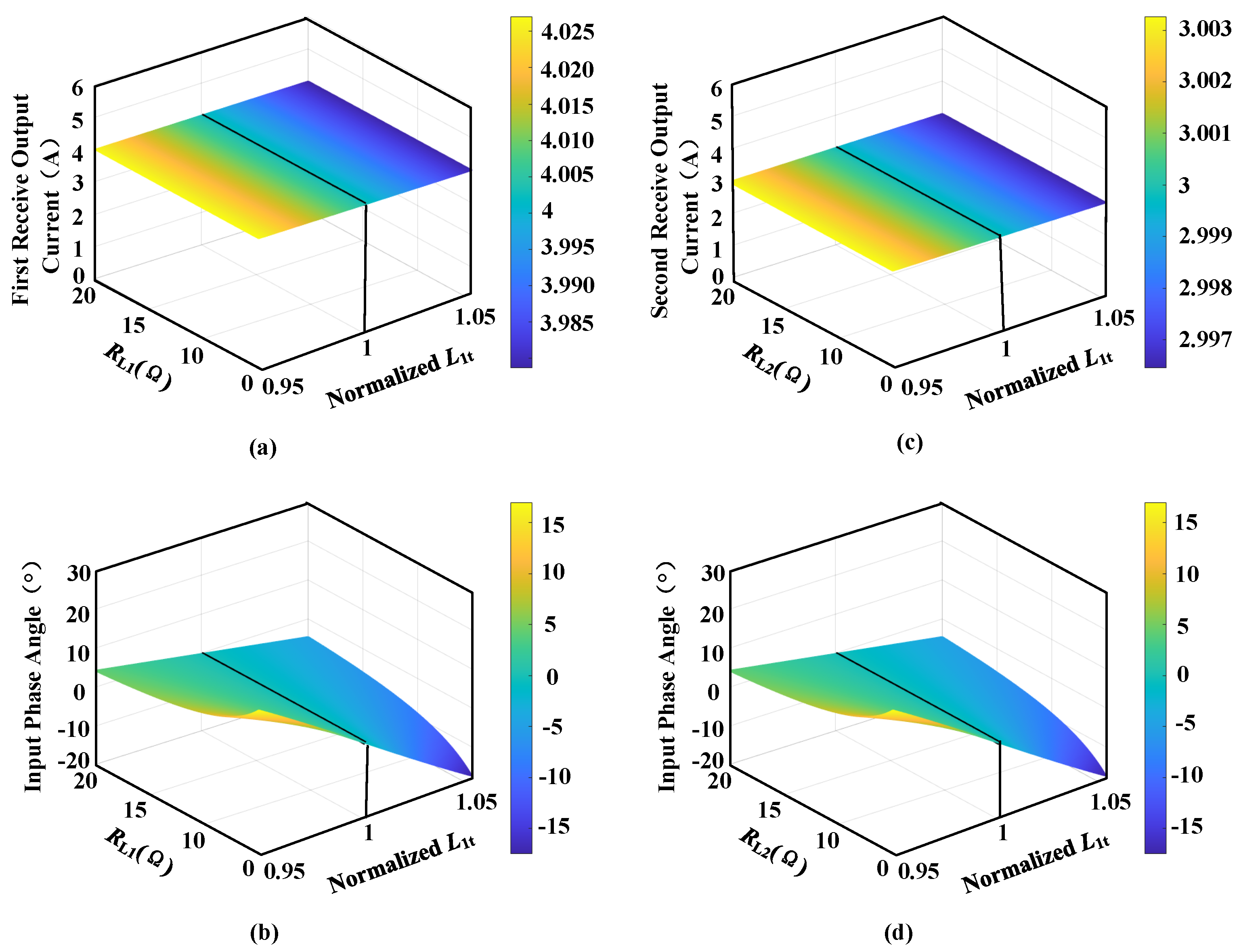
4. Simulation Experiment Verification

This paper summarizes the method of designing the parameters and designs a set of circuit parameters, as shown in Table 1. According to the designed parameters, the relationship curves between the output current of the first receiver of the system, the output current of the second receiver, and the input impedance angle under different loads and the frequency are obtained, as shown in Figure 7. It can be clearly seen that when the operating frequency of the system is 85 kHz, the system can achieve CC output that is independent of the loads of the first receiver and the second receiver under the condition of achieving ZPA operation. Through the above simulation analysis, the basic output characteristics of the proposed dual-output WPT system are verified.
In order to reduce the conduction loss of MOSFETs in high-frequency inverters, the method of changing the value of compensation components in [31] is used to make the input impedance of the system weakly inductive, thereby achieving ZVS operation and further improving the system efficiency. Figure 8, Figure 9, Figure 10, Figure 11 and Figure 12 show the effects of normalized C P , C S , C T , C 1 , and L 1 on the two output currents and input impedance angle in the system, respectively. It can be clearly seen from the figure that the input impedance angle of the system is linearly related to the normalization of C P , C S , C T , and L 1 . Therefore, ZVS operation can be achieved by increasing C P , C S , and C T and reducing L 1 . However, keeping the CC output unaffected by the changes in compensation components is also an important indicator for achieving ZVS operation. It can be concluded from the figure that the output current of the system is not affected by the normalized C S and L 1 . Therefore, the system can achieve ZVS operation by adjusting C S and L 1 .

5. Experimental Verification

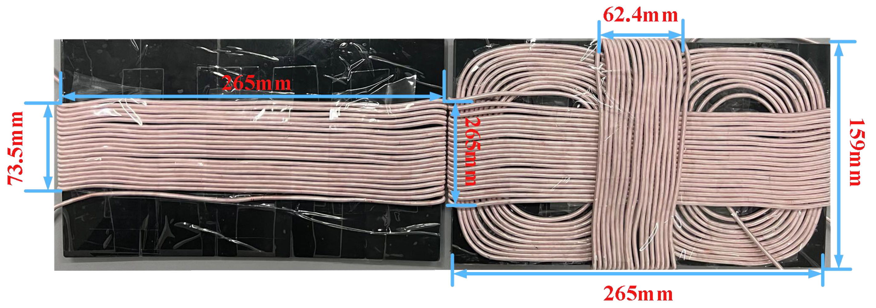
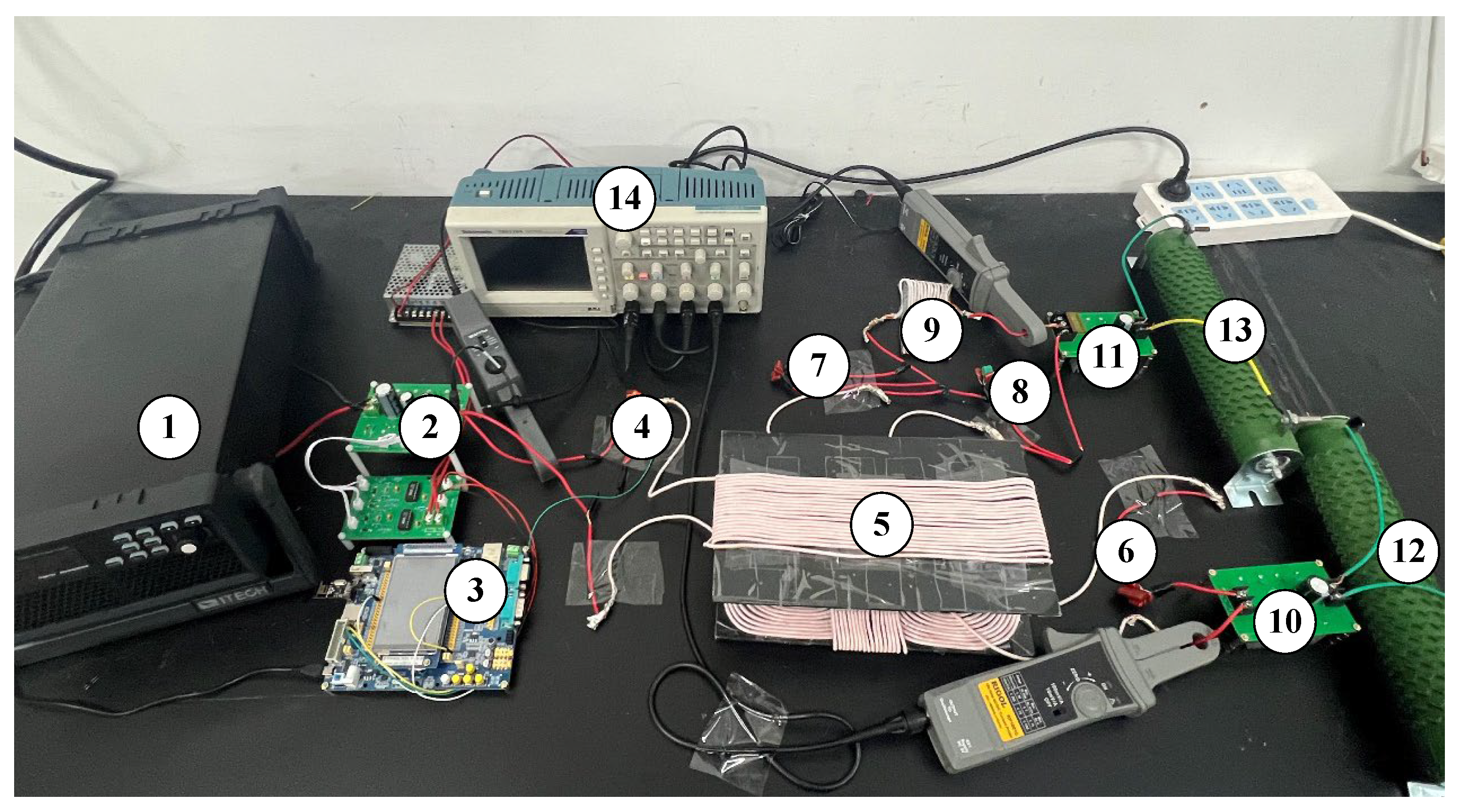
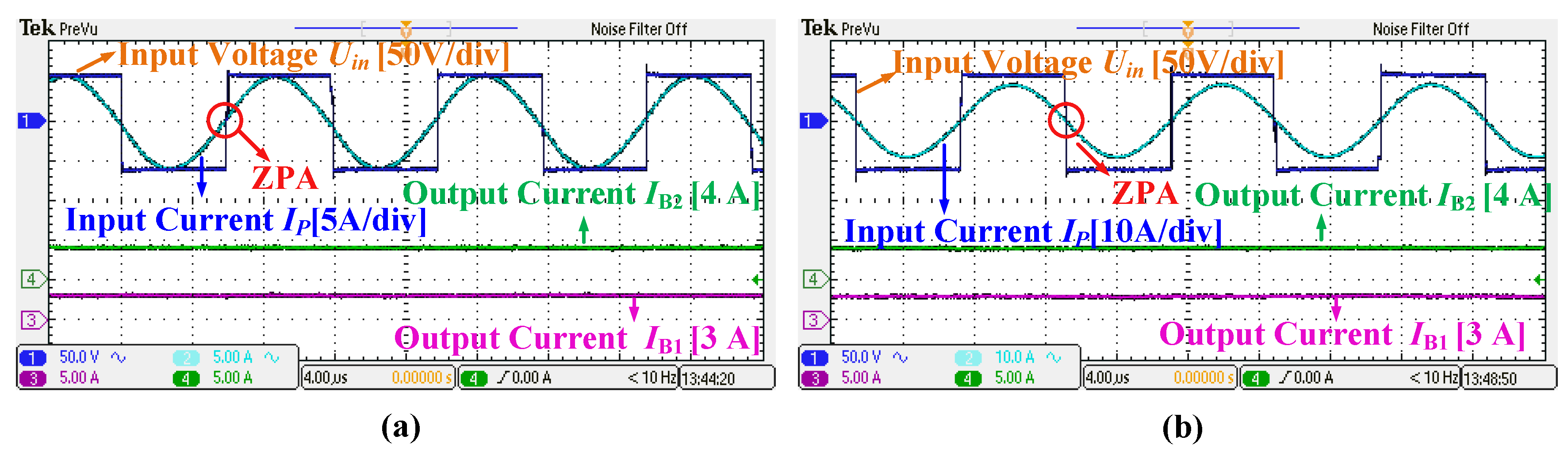
5.1. Experimental Prototype

The structure and placement of the WPT system coil will affect the power and transmission capacity of the WPT system. Therefore, for the magnetic coupler proposed in Section 2, the coil’s dimensions are impacted by the space available for installation in the electrical equipment. The dimensions of the magnetic coupler that complies with the dual-output WPT system are shown in Figure 13. The transmitter coil is integrated on the transmitting-side ferrite board in the form of a solenoid coil with a size of 265 mm × 73.5 mm. The first receiving coil is composed of a series connection of a DD type and a solenoid coil. The size of the DD coil is 265 mm × 159 mm, the size of the solenoid coil is 265 mm × 73.5 mm. The second receiving coil is a solenoid coil with a size of 159 mm × 62.4 mm, and its direction is perpendicular to the direction of the solenoid coil of the first receiver. The first receiving coil and the second receiving coil are integrated on the receiving-side ferrite plate. The dimensions of the ferrite disks on both the transmitter and receiver sides are 265 mm × 159 mm × 2.5 mm. The detailed dimension parameters are shown in Table 2.
To verify the correctness of the theoretical analysis of the proposed dual-output WPT system, a verification experimental prototype was built, as shown in Figure 14. The experimental prototype consists of the following components: a DC input voltage source; a HFI composed of four MOSFETs (IRFP250N), an STM32F407 microcontroller for generating drive signals; a series compensation capacitor C P ; a magnetic coupler; the compensation capacitor C S , C T , and C 1 ; a compensation inductor L 1 ; a rectifier composed of four diodes (DSE120−16A); a load resistor; and an oscilloscope. These components are labeled sequentially from 1 to 14. The detailed design parameters are shown in Table 3.

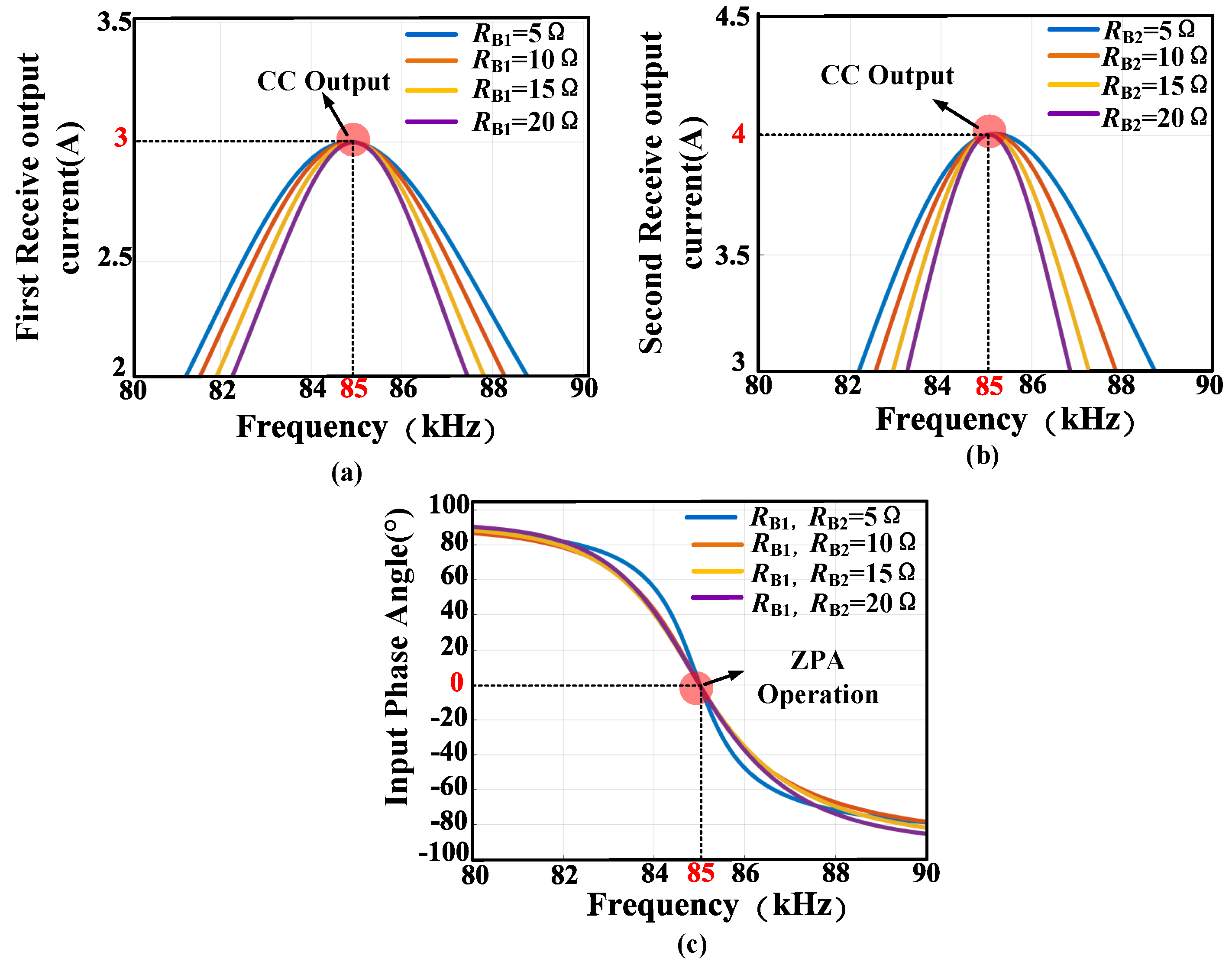
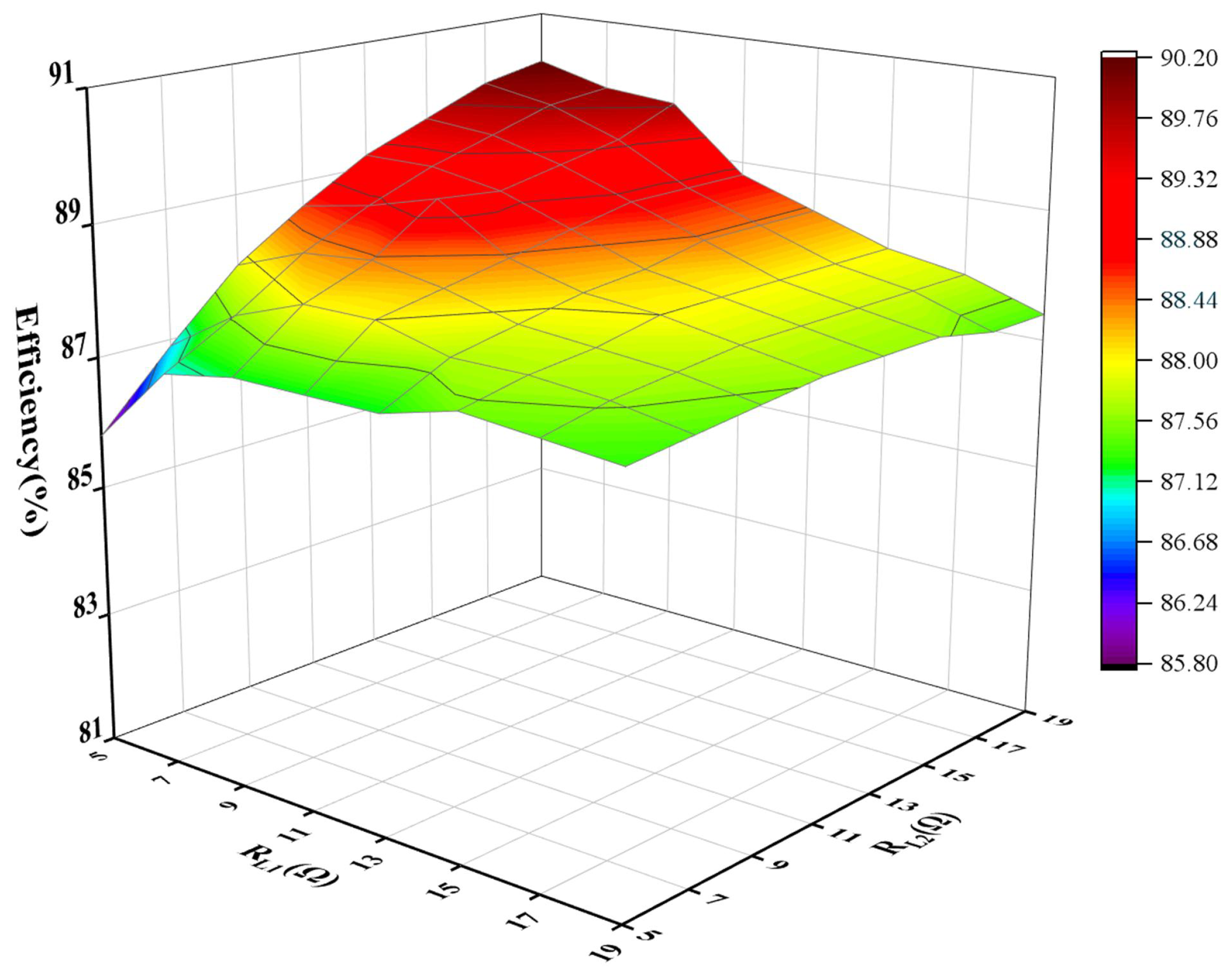
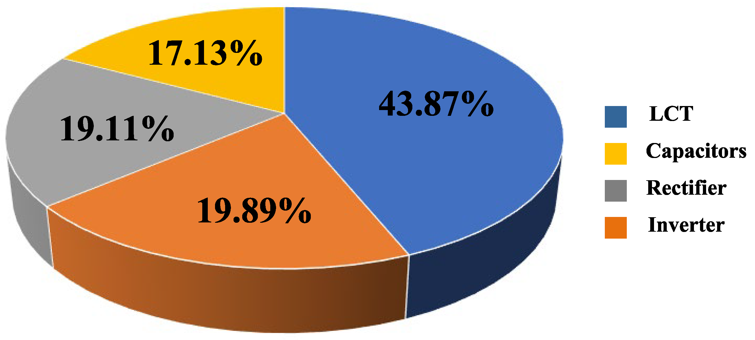
5.2. Experimental Results

Figure 15 shows the waveforms of the output voltage U i n , the output current I P , the first receiver output current I B 1 , and the second receiver output current I B 2 of the HFI. In Figure 15a, the load resistances R B 1 and R B 2 of the first receiver and the second receiver are set to 5 Ω and 10 Ω , respectively. In Figure 15b, R B 1 and R B 2 are set to 10 Ω and 15 Ω . It can be clearly seen that from Figure 15, under the condition of keeping the output current of 3 A and 4 A constant for I B 1 and I B 2 . In addition, the output voltage U i n of HFI is always in phase with the output current I P , which shows that the system realizes ZPA operation.
According to the ZVS analysis in Section 4, the series compensation capacitor of the first receiver is set to C S t Z V S , and Figure 16 shows the waveforms of U i n , I P , the first receiver output current I B 1 , and the second receiver output current I B 2 . In Figure 16a, the load resistors R B 1 and R B 2 of the first receiver and the second receiver are set to 5 Ω and 10 Ω , respectively. In Figure 16b, R B 1 and R B 2 are set to 10 Ω and 15 Ω . As can be seen from Figure 16, under the condition of keeping the output current of 3 A and 4 A constant for I B 1 and I B 2 , U i n leads I P by a small angle, that is, Z i n is weakly inductive. That is, the system achieves ZVS operation without affecting the constant current output characteristics, which is independent of the load, further improving the system efficiency.
Figure 17 shows the DC–DC efficiency surface measured under different load conditions. It can be clearly seen that the peak efficiency of the proposed system reaches 90.2 % , and it can maintain a high efficiency and continuous output.
When loads R B 1 and R B 2 are changed from 5 Ω to 19 Ω in steps of 2 Ω , 49 different combinations are measured, and the corresponding power distribution surface diagram is shown in Figure 18. It can be clearly seen that through reasonable parameter design, the power distribution ratio of the first receiver and the second receiver can satisfy the complementary relationship and change evenly with the changes of the two loads.
Figure 19 shows the power loss distribution of each system component measured under the conditions of load resistance R B 1 being 5 Ω and load resistance R B 1 being 19 Ω . Determining the proportional loss of each system component needs to be achieved by measuring the internal resistance of each system component and the resonant current flowing through them, a method similar to that proposed in [32,33]. As can be observed from the pie chart, there are significant losses in the HFI and rectifier. Therefore, in practical applications, researchers can refer to the loss distribution shown in Figure 19 to guide further optimization.
In addition, in order to reflect the advantages of the energy transfer dual-output WPT system compared with previous studies, the comparison results are shown in Table 4.
(1) The proposed WPT system uses its own structural characteristics to achieve dual CC outputs. Compared with [16,17,20,23,24,26], it avoids additional circuits and complex control, making the system simpler.
(2) The proposed WPT system adopts a special magnetic coupler design, which can achieve theoretical complete decoupling, which is an advantage compared with [16,17,20,23,24,26,30]. In addition, the first receiver coil and the second receiver coil are integrated together on the receiving side ferrite plate, which can achieve a higher space utilization, which is an advantage compared with [16,17,20,24].

6. Conclusions

This paper proposes a WPT system based on integrated decoupling coils, which can achieve CC outputs of different specifications regardless of the load. In addition, in order to save installation space and eliminate the influence of cross coupling, the proposed magnetic coupling device has the characteristics of natural decoupling, and uses coil optimization methods to reduce the complexity of the design and improve the spatial utilization rate of the system. In order to reduce conduction loss and further improve system efficiency, by slightly reducing the compensation capacitor C S t , the system can achieve ZVS operation without affecting the output characteristics. Compared with the traditional WPT system that realizes dual outputs, the proposed system adopts a simple magnetic coupler decoupling design and coil optimization method. It can achieve stable output of different specifications based on energy transfer without complex control methods and has a higher space utilization. It is worth emphasizing that due to the compact design and multi-output characteristics of the system, it can be applied to fields such as multi-output chargers for LED. Finally, it is recommended to expand WPT systems with different output types in the future.

Author Contributions

Conceptualization, L.Y. (Le Yu) and S.X.; methodology, X.Z.; software, J.W.; validation, L.Y. (Le Yu), S.X., L.Y. (Lin Yang), J.W. and X.Z.; formal analysis, L.Y. (Le Yu); investigation, L.Y. (Lin Yang); resources, L.Y. (Lin Yang); data curation, S.X.; writing—original draft preparation, S.X.; writing—review and editing, S.X.; visualization, X.Z.; supervision, J.W.; project administration, L.Y. (Lin Yang); funding acquisition, J.W. All authors have read and agreed to the published version of the manuscript.

Funding

This research was funded by “Harbin manufacturing science and technology innovation talent project 2022HBRCCG006”.

Data Availability Statement

Data are contained within the article.

Conflicts of Interest

The authors declare no conflicts of interest.

References

  1. Li, Y.; Mai, R.; Liu, Y.; He, Z. Efficiency optimising strategy for dual-coupled transmitters based WPT systems. Electron. Lett. 2016, 52, 1877–1879. [Google Scholar] [CrossRef]
  2. Li, Y.; Hu, J.; Li, X.; Cheng, K.-W.-E. A Flexible Load-Independent Multi-Output Wireless Power Transfer System Based on Cascaded Double T-Resonant Circuits: Analysis, Design and Experimental Verification. IEEE Trans. Circuits Syst. Regul. Pap. 2019, 66, 2803–2812. [Google Scholar] [CrossRef]
  3. Lillholm, M.-B.; Dou, Y.; Chen, X.; Zhang, Z. Analysis and Design of 10-MHz Capacitive Power Transfer With Multiple Independent Outputs for Low-Power Portable Devices. IEEE J. Emerg. Sel. Top. Power Electron. 2022, 10, 149–159. [Google Scholar] [CrossRef]
  4. Cai, C.; Saeedifard, M.; Wang, J.; Zhang, P.; Zhao, J.; Hong, Y. A Cost-Effective Segmented Dynamic Wireless Charging System With Stable Efficiency and Output Power. IEEE Trans. Power Electron. 2022, 37, 8682–8700. [Google Scholar] [CrossRef]
  5. Jafari, H.; Moghaddami, M.; Olowu, T.-O.; Sarwat, A.-I.; Mahmoudi, M. Virtual Inertia-Based Multipower Level Controller for Inductive Electric Vehicle Charging Systems. IEEE J. Emerg. Sel. Top. Power Electron. 2021, 9, 7369–7382. [Google Scholar] [CrossRef]
  6. Cai, C.; Wang, J.; Wan, L.; Wang, C. Optical Fiber Composite Winding for In Situ Thermal Monitoring of Transmitter Magnetic Mechanism in Long-Track DWPT Systems. IEEE Trans. Instrum. Meas. 2024, 73, 1–4. [Google Scholar] [CrossRef]
  7. Pahlavan, S.; Ashtiani, S.-J.; Saad, M.; Soon, T.-K.; Chong, W.-T. Rotation-Tolerant Wireless Power Transmission Scheme with Smart Positioning for Cognitive Research on Moving Animals. IEEE Trans. Biomed. Circuits Syst. 2024, 18, 123–130. [Google Scholar] [CrossRef]
  8. Pahlavan, S.; Shooshtari, M.; Ashtiani, S.-J. Star-Shaped Coils in the Transmitter Array for Receiver Rotation Tolerance in Free-Moving Wireless Power Transfer Applications Energies. Energies 2022, 15, 8643. [Google Scholar] [CrossRef]
  9. Zhou, R.; Chung, H.; Zhang, R. An inductive power transfer system for driving multiple OLED light panels. IEEE Trans. Power Electron. 2016, 31, 7131–7147. [Google Scholar] [CrossRef]
  10. Stankiewicz, J.-M. Analysis of the Wireless Power Transfer System Using a Finite Grid of Planar Circular Coils Energies. Energies 2023, 16, 7651. [Google Scholar] [CrossRef]
  11. Vu, V.-B.; Phan, V.-T.; Nguyen, D.-T.; Logenthiran, T.; Naayagi, R.-T. Design and implementation of a multi-output inductive charger for electric vehicles. In Proceedings of the 2016 IEEE International Conference on Sustainable Energy Technologies, Hanoi, Vietnam, 14–16 November 2016; pp. 414–419. [Google Scholar]
  12. Yang, C.; Li, M.; Yang, B.; Chen, S.; Li, Q.; He, Z.; Mai, R. Variable-Parameter T-Circuit-Based IPT System Charging Battery With Constant Current or Constant Voltage Output. IEEE Trans. Power Electron. 2019, 35, 1672–1684. [Google Scholar]
  13. Jang, Y.; Jovanovic, M.-M. A Contactless Electrical Energy Transmission System for Portable-telephone Battery Chargers. IEEE Trans. Ind. Electron. 2003, 31, 520–527. [Google Scholar] [CrossRef]
  14. Hu, J.; Lu, F.; Zhu, C.; Cheng, C.Y.; Chen, S.L.; Ren, T.J.; Mi, C.C. Hybrid Energy Storage System of an Electric Scooter Based on Wireless Power Transfer. IEEE Trans. Ind. Inform. 2018, 14, 4169–4178. [Google Scholar] [CrossRef]
  15. McDonough, M. Integration of Inductively Coupled Power Transfer and Hybrid Energy Storage System: A Multiport Power Electronics Interface for Battery-Powered Electric Vehicles. IEEE Trans. Power Electron. 2015, 30, 6423–6433. [Google Scholar] [CrossRef]
  16. Yu, K.-O.; Jossel Mindoro Maestro, R.; De Leon, M.-T.-G. A Study on the Effectiveness of Using a Hybrid Topology in Improving the Power Efficiency and Voltage Regulation over a Wide Input Range of DC-DC Converters. In Proceedings of the TENCON 2018–2018 IEEE Region 10 Conference, Jeju, Republic of Korea, 28–31 October 2018; pp. 2104–2109. [Google Scholar]
  17. Li, Y.; Hu, J.; Chan, K.W.; Eric Cheng, K.-W.; Liu, M. A Flexible Load-Independent Multi-Output Wireless Power Transfer System Based on Double-T Resonant Circuit Technique. In Proceedings of the 2018 IEEE Energy Conversion Congress and Exposition (ECCE), Portland, OR, USA, 23–27 September 2018; pp. 3593–3596. [Google Scholar]
  18. Casanova, J.-J.; Low, Z.-N.; Lin, J. A Loosely Coupled Planar Wireless Power System for Multiple Receivers. IEEE Trans. Ind. Electron. 2009, 56, 3060–3068. [Google Scholar] [CrossRef]
  19. Cannon, B.-L.; Hoburg, J.F.; Stancil, D.D.; Goldstein, S.C. Magnetic Resonant Coupling As a Potential Means for Wireless Power Transfer to Multiple Small Receivers. IEEE Trans. Power Electron. 2009, 24, 1819–1825. [Google Scholar] [CrossRef]
  20. Liu, X.; Han, W.; Liu, C.; Pong, P. Marker-free coil-misalignment detection approach using TMR sensor array for dynamic wireless charging system of electric vehicles. IEEE Trans. Magn. 2018, 54, 4002305. [Google Scholar] [CrossRef]
  21. Zhang, J.; Yuan, X.; Wang, C.; He, Y. Comparative analysis of two-coil and three-coil structures for wireless power transfer. IEEE Trans. Power Electron. 2017, 32, 341–352. [Google Scholar] [CrossRef]
  22. Mai, R.; Luo, Y.; Yang, B.; Song, Y.; Liu, S.; He, Z. Decoupling circuit for automated guided vehicles IPT charging systems with dual receivers. IEEE Trans. Power Electron. 2020, 35, 6652–6657. [Google Scholar] [CrossRef]
  23. Wang, X.; Xu, J.; Ma, H.; Zhang, Y. A Reconstructed S-LCC Topology With Dual-Type Outputs for Inductive Power Transfer Systems. IEEE Trans. Power Electron. 2020, 35, 12606–12611. [Google Scholar] [CrossRef]
  24. Zhong, W.; Hui, S.Y.R. Auxiliary circuits for power flow control in multifrequency wireless power transfer systems with multiple receivers. IEEE Trans. Power Electron. 2015, 30, 5902–5910. [Google Scholar] [CrossRef]
  25. Zhang, Y.; Lu, T.; Zhao, Z.; He, F.; Chen, K.; Yuan, L. Selective wireless power transfer to multiple loads using receivers of different resonant frequencies. IEEE Trans. Power Electron. 2015, 30, 6001–6005. [Google Scholar] [CrossRef]
  26. Chen, W.; Li, H.; Lu, W. Decoupling design of multi-coil wireless power transfer system with metal insulator. In Proceedings of the 2017 IEEE PELS Workshop on Emerging Technologies: Wireless Power Transfer (WoW), Chongqing, China, 20–22 May 2017; pp. 30–33.
  27. Zhou, Z.; Shi, Q.; Cheng, C.; Li, W.; Deng, Z.; Li, F.; Mi, C. A Multi-load wireless power transfer system with constant voltage outputs using S-LCC compensation. In Proceedings of the 2019 22nd International Conference on Electrical Machines and Systems (ICEMS), Harbin, China, 11–14 August 2019; pp. 11–14. [Google Scholar]
  28. Wang, H.-S.; Cheng, K.-W.-E. Analysis, design, and validation of a decoupled double-receiver wireless power transfer system with constant voltage outputs for industrial power supplies. IEEE Trans. Ind. Informatics 2019, 19, 362–370. [Google Scholar] [CrossRef]
  29. Pang, H.; Chau, K.T.; Han, W.; Liu, W.; Zhang, Z. Decoupled-Double D Coils Based Dual-Resonating-Frequency Compensation Topology for Wireless Power Transfer. IEEE Trans. Magn. 2022, 58, 1–7. [Google Scholar] [CrossRef]
  30. Pratik, U.; Varghese, B.-J.; Azad, A.; Pantic, Z. Optimum Design of Decoupled Concentric Coils for Operation in Double-Receiver Wireless Power Transfer Systems. IEEE J. Emerg. Sel. Top. Power Electron. 2018, 7, 1982–1998. [Google Scholar] [CrossRef]
  31. Qu, X.; Chu, H.; Wong, S.-C.; Tse, C.-K. An IPT battery charger with near unity power factor and load-independent constant output combating design constraints of input voltage and transformer parameters. IEEE Trans. Power Electron. 2019, 34, 7719–7727. [Google Scholar] [CrossRef]
  32. Wang, J.; Sun, Q.; Li, Y. A CV-type WPT system based on CLC-N compensation with compact receiver. Int. J. Circuit Theory Appl. 2024. early access. [Google Scholar] [CrossRef]
  33. Yang, L.; Dong, K.; Wang, Y.; Cai, C.; Zhou, X. Analysis, Design, and Validation of a Dual-Channel High-Power WPT System Based on Bilateral Coil Decoupling. IEEE J. Emerg. Sel. Top. Power Electron. 2024, 12, 4288–4295. [Google Scholar] [CrossRef]
Figure 1. Distribution of magnetic flux in two solenoid coils oriented perpendicularly to each other.
Electronics 13 03371 g001
Figure 2. Schematic diagram of the magnetic flux distribution of two perpendicular DD coils and a solenoid coil.
Electronics 13 03371 g002
Figure 3. Proposed magnetic coupler structure and optimization method.
Electronics 13 03371 g003
Figure 4. The schematic diagram of magnetic coupling for the magnetic coupler.
Electronics 13 03371 g004
Figure 5. Overall architecture of the proposed WPT system based on integrated decoupling coils.
Electronics 13 03371 g005
Figure 6. Equivalent circuit diagram of the WPT system.
Electronics 13 03371 g006
Figure 7. Frequency sweep curves of a dual−output WPT system under different loads. (a) Output current of the first receiver. (b) Output current of the second receiver. (c) Input impedance angle.
Electronics 13 03371 g007
Figure 8. Normalized capacitor C P t and R B 1 and (a) output current, (c) input phase. Normalized capacitor C P t and R B 2 and (b) output current, (d) input phase angle.
Electronics 13 03371 g008
Figure 9. Normalized capacitor C S t and R B 1 and (a) output current, (c) input phase. Normalized capacitor C S t and R B 2 and (b) output current, (d) input phase angle.
Electronics 13 03371 g009
Figure 10. Normalized capacitor C T t and R B 1 and (a) output current, (c) input phase. Normalized capacitor C T t and R B 2 and (b) output current, (d) input phase angle.
Electronics 13 03371 g010
Figure 11. Normalized capacitor C 1 t and R B 1 and (a) output current, (c) input phase. Normalized capacitor C 1 t and R B 2 and (b) output current, (d) input phase angle.
Electronics 13 03371 g011
Figure 12. Normalized capacitor L 1 t and R B 1 and (a) output current, (c) input phase. Normalized capacitor L 1 t and R B 2 and (b) output current, (d) input phase angle.
Electronics 13 03371 g012
Figure 13. Proposed magnetic coupler structure.
Electronics 13 03371 g013
Figure 14. Constructed verification experimental prototype.
Electronics 13 03371 g014
Figure 15. Experimental waveforms of U i n , I P , I B 1 , and I B 2 under ZPA conditions (a) R B 1 = 5 Ω , R B 2 = 10 Ω , (b) R B 1 = 10 Ω , R B 1 = 15 Ω .
Electronics 13 03371 g015
Figure 16. Experimental waveforms of U i n , I P , I B 1 and I B 2 under ZVS conditions (a) R B 1 = 5 Ω , R B 2 = 10 Ω , (b) R B 1 = 10 Ω , R B 1 = 15 Ω .
Electronics 13 03371 g016
Figure 17. Total DC-DC efficiency surface under different load combinations.
Electronics 13 03371 g017
Figure 18. Power Distribution Ratio Surface (a) The power distribution ratio of the first receiver, (b) The power distribution ratio of the second receiver.
Electronics 13 03371 g018
Figure 19. Power loss distribution of each system component measured under aligned conditions with a load resistor R B 1 of 5 Ω and load resistor R B 1 of 19 Ω .
Electronics 13 03371 g019
Table 1. Theoretical design parameters of the energy transfer dual-output WPT system.
ParametersValueParametersValue
f85 kHzE60 V
L P 205.87 μ H C P 16.65 nF
L S 295.78 μ H C S 11.72 nF
L T 136.53 μ H C T 31.62 nF
L 1 27 μ H C 1 129.36 nF
M PS 30.56 μ H M ST 37.21 μ H
Table 2. The detailed dimension parameters of the energy transfer dual-output WPT system.
ParameterSpecific Information
Litz wire500 strands with diameter of 3.2 mm
transmitting side coilSize of 265 mm × 73.5 mm, 20 turns
The first receiving DD coilSize of 159 mm × 265 mm, 10 turns
The first receiving solenoid coilSize of 265 mm × 73.5 mm, 20 turns
The second receiving coilSize of 159 mm × 62.4 mm, 17 turns
Air gap60 mm
Ferrite plate PC 40Size of 159 mm × 265 mm × 2.5 mm
Table 3. Theoretical design parameters of the energy transfer dual output WPT system.
ParametersValueParametersValue
f85 kHzE60 V
L P 206.44 μ H C P 16.98 nF
L S 296.78 μ H C S 11.81 nF
L T 137.02 μ H C T 31.56 nF
L 1 27.13 μ H C 1 129.78 nF
M PS 30.36 μ H M ST 37.53 μ H
C St ZVS 11.51 nF
Table 4. Comparison of the results of this study with previous similar studies.
Proposed inRef. [16]Ref. [17]Ref. [18]Ref. [23]Ref. [24]Ref. [26]Ref. [30]This Work
Additional circuits and control methodsYesYesYesYesYesYesNoNo
High space utilizationNoNoNoNoNoNoNoYes
Theoretically completely decoupledNoNoNoYesNoYesYesYes
Simple magnetic coupler designNoNoNoNoNoNoYesYes
Disclaimer/Publisher’s Note: The statements, opinions and data contained in all publications are solely those of the individual author(s) and contributor(s) and not of MDPI and/or the editor(s). MDPI and/or the editor(s) disclaim responsibility for any injury to people or property resulting from any ideas, methods, instructions or products referred to in the content.

