Abstract
Sync word-based frame synchronization is an established method of frame synchronization that is employed in many low-resource applications because of its simplicity, and it involves the attachment of sync words (digital binary sequences) to the frames, which are then used for detection. Despite its simplicity, the method is underutilized today because there is no available hardware scheme that can perform correlation-based sync word frame synchronization with long sync words (>80 bits) efficiently. For this reason, the sync word methods that are used typically employ sync words of shorter lengths (<50 bits) with limited accuracy. This article introduces a highly modifiable, minimalist hardware architecture that performs correlation-based sync word frame synchronization using long sync words with evident accuracy gains over existing methods. As a bonus, the architecture not only detects the frame but also captures its payload regardless of size. Its low complexity allows for its deployment at a low cost in terms of hardware resources and power while providing high bit rates. Its flexibility is demonstrated by using a low-cost FPGA for implementation.
1. Introduction
Frame synchronization is the detection of valid data frames from an incoming transmission and is an integral part of digital communications. In this paper, we focus specifically on frame synchronization based on sync word detection. This method entails the injection of certain sync words (binary sequences) within the frames, which are then detected with digital correlation. Pioneered by Barker in [1], it is the most basic form of frame synchronization still used in applications today, such as radar sensors [2]. Barker used specific sync words called Barker sequences, which possess the ideal autocorrelation property, meaning that the autocorrelation sidelobes are as small as possible. It was widely believed that this was the optimal method of frame synchronization until Massey introduced the maximum likelihood rule by adding a non-linear correction term to Barker’s correlator to account for the data surrounding the sync words [3]. Massey also developed an easily implementable approximation of the scheme with negligible performance loss [4]. Since then, more variations have been proposed, such as observing sync words in multiple frames [5] or developing novel sequential algorithms [6] based on likelihood metrics. It has also been shown that even though the sync word method is old, it still competes in terms of performance with more sophisticated contemporary frame synchronization methods like joint LDPC frame synchronization [7].
In this paper, we introduce a novel minimalist frame synchronization architecture for sync word-based frame synchronization. We forego Massey’s maximum likelihood rule and instead achieve high frame detection accuracy by using simple correlation with very large sync words (>80 bits). We specifically design the architecture in a way that allows it to perform correlation on long sync words at high bit rates while using the least possible amount of resources and power. Until now, this scheme is the only method that can achieve large sync word correlation detection in a practically implementable way. The architecture not only detects the frame but also, as a bonus, captures its payload regardless of length without changing it as a circuit. If the frame consists of a header part and a data part (which is generally the standard), capture of the payload entails the isolation of the data part and its delivery to the receiving processing system. Its flexibility is demonstrated by using a low-cost commercial FPGA for implementation. As in most of the literature pertaining to sync word frame synchronization, the channel is AWGN, and we assume that symbol synchronization has already been achieved [5] and the architecture only deals with frame synchronization.
The paper consists of five sections. The second section is dedicated to the preliminaries necessary to understand the architecture’s functionality. The third section contains a description of the architecture. The fourth section presents the result of the implementation and testing as well as comparisons with other methods. The article ends with a conclusion.
2. Preliminaries
The architecture achieves synchronization by detecting sync words through digital correlation. Different forms and lengths of sync words will produce different results. Data surrounding the sync word can also be manipulated to boost detection accuracy (reduce the size of correlation sidelobes). In this work, the marker sequences used to identify the frames (sync word and surrounding data) are of the form akblck (transmitted from right to left, ck is first and ak last), where ak and ck are sequences of length k bits, and bl is a sequence of length l bits with l >> 2 × k; bl is random (randomly generated, which means every bit has an equal chance of being ‘0’ or ‘1’), but ak and ck must be the last and first k bits (respectively) of bl inversed (ak = NOT (last k bits of bl), ck = NOT (first k bits of bl)); bl sequence is the sync word the architecture uses to detect the frame, and sequences ak and ck are the manipulated surrounding data; ak and ck are not used by the architecture for detection. Their role is to ensure that the correlation values in all other positions except the first bit of bl remain low, boosting the architecture’s detection accuracy. This phenomenon is easier to observe and has a much stronger effect when bl is long (>70 bits). This is how ak and ck influence the outcome of the detection indirectly (without being detected themselves).
Once the bl sequence is generated, it is considered predefined (i.e., known to both transmitter and receiver). For example, suppose that l = 32 bits. A random 32-bit sequence as generated by a random binary sequence generator is 11001010101110101110001100000111. Once the sequence is generated, it remains random in a mathematical sense (created by a random generator engine); however, it is now predefined and known to both the receiver and transmitter. Predefined in the context of the article means that bl is generated before the communication takes place and is used during it.
This form of sync word and surrounding data are not optimal. It is simply what was used since it showed good detection results and is very easy to construct. Other sequences that have much better correlation properties, such as those constructed in [8], can also be used at the user’s discretion. The form of the entire frame is payloadpakblck, transmitted from right to left. Payloadp is the data bits of the frame (length p bits), and akblck is the extra bits needed for detection by the architecture and can be considered as the frame marker. Detection of the bl sequence (sync word) is based on the following three principles:
- To calculate the number of similar elements in respective positions between two vectors v1 and v2 of the same size s, we apply the XNOR operation on elements in respective positions (j position in both v1 and v2), and we add the products (digital correlation). The result of the summation sum represents how many similar elements the two vectors have. When the value of the sum is high, the two vectors are similar. When the value of the sum is low, the two vectors are not similar. Essentially, it is the opposite of Hamming distance;
- If we have a much larger vector v3 of size z where z >> s, we can use the process in principle 1 to determine whether v1 exists inside v3. This is achieved by applying it in all possible positions; v1 can be inside v3. There are z − s + 1 possible positions for v1 inside v3, which are s−1 down to 0, s down to 1, s + 1 down to 2…. z − 2 down to z − s − 1, and z − 1 down to z − s. This means that principle 1 is applied z − s + 1 times, and for every iteration, v1 is v1, and v2 corresponds to the vector constructed by elements inside v3 of the respective positions (for example, elements in positions s−1 down to 0 for the first iteration). The process produces z − s + 1 values sumi. If any of these values equals s or is close to s, then this means that v1 or a vector that resembles it was detected inside v3. This process works no matter how large the size z of v3 is;
- For the architecture, v3 is the incoming transmission bitstream, and v1 is sequence bl. It detects bl inside v3 using principle 2 and captures the payload of the frame.
These three principles form the basis for the function of the architecture, and henceforth, they will be referenced with parenthesis ((1) referring to principle 1). The input of the architecture is the digital stream, which results from the demodulation of the incoming transmission. Without loss of generality, we assume that the input is given as a parallel bit-vector of size l (same size as sequence bl). In other words, instead of receiving one bit at f frequency, the architecture receives l bits at fop = f/l frequency, and its total bit rate is fop × l. We also assume that if the parallel input bit vector elements are l−1 down to 0, the bit in position 0 was transmitted earlier in the incoming bitstream timeline than the bit in position l−1. Figure 1 is the visual representation of how the architecture “sees” the incoming data stream. Time flows to the left, so samples to the right were transmitted earlier.
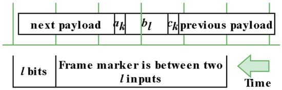
Figure 1.
Real-time reception of the input. It is separated by blocks of l bits. The frame header sequence akblck (<2 × l) is between two inputs.
The bitstream is separated into blocks of l bits (l − 1 down to 0), which is the size of the input. We can clearly see that bl is always between two inputs (2 × l > l). The architecture isolates these 2 × l bits each time, correlates them with the predefined bl, finds the start of the payload, and captures it. The rare case when the bl header is perfectly aligned with an input sample is also considered. For testing, AWGN is the channel model, and 16QAM is the modulation. This will be expanded upon in the testing section.
3. Architecture
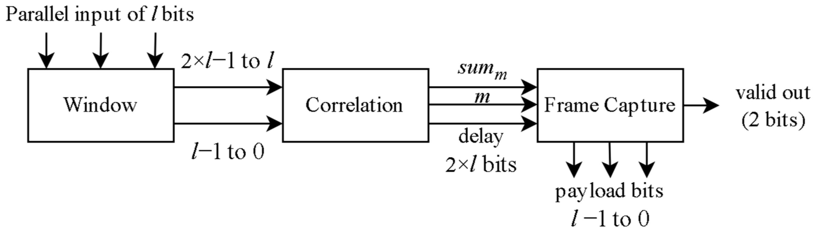
The architecture is comprised of three modules: Window Module, Correlation Module, and Payload Capture Module. The Window Module consists of a 2 × l bit register that it uses to isolate the area of the incoming stream in which sequence bl is located. It sends the contents of this register to the Correlation Module so that the position of the payload can be calculated. The Correlation Module correlates the predefined stored bl sequence with the area isolated by the Window Module (in accordance with (2)) and calculates two values, summ and m; summ is the maximum value of all correlation values in the current window (of 2 × l bits), and m is the position it was detected in. Apart from these two values, the Correlation Module also provides the synchronized input, i.e., the contents of the Window Module register, for which the values are calculated, to the Payload Capture Module for correct synchronization. The Payload Capture Module uses summ and m to determine the position of the payload and the synchronized input to capture it. A valid out signal is used to notify the rest of the system of successful capture. The entirety of the receiver architecture can be seen in Figure 2.
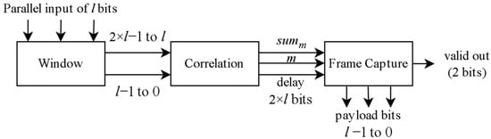
Figure 2.
Overview of the system.
3.1. Window Module
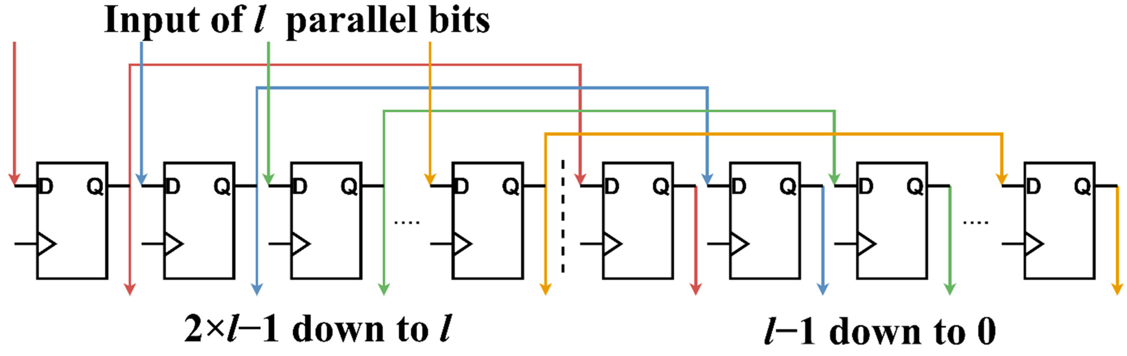
The Window Module isolates a specific region of the incoming bitstream so that the Correlation Module can determine whether bl (and, as a result, the frame) was detected in that specific region. The module consists of a 2 × l bit register (memory elements 2 × l − 1 down to 0). The l-bit input enters the left half of the register (elements 2 × l − 1 down to l) from the input pins in clock cycle t. In clock cycle t + 1, the contents of the left half are transferred to the right half (elements l − 1 down to 0) while keeping their order, and the new bits enter the left half. Essentially, memory elements (D flip flops) that are l positions apart are connected serially. The Window module can be seen in Figure 3.
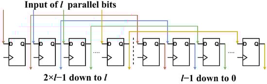
Figure 3.
The figure is color-coded. Elements connected with the same-colored wire are connected serially.
A 2 × l is the minimum number of memory elements needed to capture the bl sequence when the size of the parallel input is l bits long. We can easily show this by considering the following. If the input vector is l bits long, the starting position of bl can be any one of these l bits, which means that all the possible positions for bl are 2 × l − 2 down to l – 1 (bl starts from bit l − 1), 2 × l − 3 down to l – 2 (bl starts from bit l − 2) … l − 1 down to 0 (bl starts from 0). Because in every clock cycle elements shift l bits, positions 2 × l − 1 down to l is the same as l − 1 down to 0 (shifted to the right by l bits) and do not need to be checked. Determining which one of these positions is the most probable one is the role of the Correlation Module.
3.2. Correlation Module
The Correlation Module is the core of the architecture and is comprised of three main subcircuits: The Parallel Adder Trees, the Selector, and the Input Delay Buffer.
The Parallel Adder Trees subcircuit performs the action described in (2). It correlates, in parallel (digitally as described in (1)), the stored bl sequence with the vectors in all possible bl positions. As mentioned, these positions are 2 × l − 2 down to l − 1, 2 × l − 3 down to l − 2 … l − 1 down to 0. The result of this process is l values sumi, the highest of which is the most probable position for bl. For each position, the correlation value sumi is calculated by using xnor gates (for the XNOR operation) and an adder tree (to calculate the summation of all XNOR outputs). Adder trees are common structures and are extensively used in many hardware designs for calculating the summation of multiple values. In our case, the adder trees have the characteristic form seen in Figure 4.
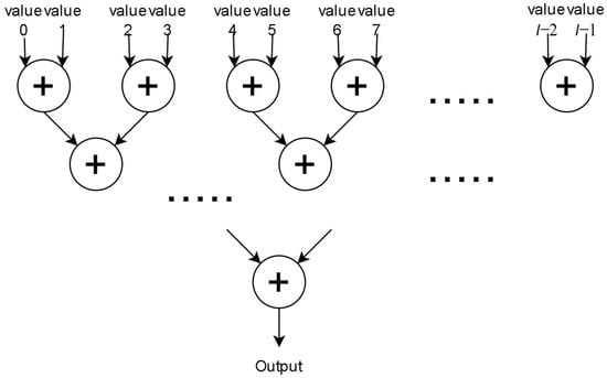
Figure 4.
Adder tree.
For the summation of l values, the trees are comprised of ceil(log2l) levels. In every level, the values calculated by previous levels are added by two, and the output of this process is given as an input to the next level. Eventually, the summations of all elements are calculated on the last level. By adding registers in between the adders, the structure becomes pipelined. Each adder tree corresponds to one value sumi, so in total, l adder trees are used. The latency of the adder tree is ceil(log2l) clock cycles.
The Selector subcircuit determines (“selects”) the highest value Summ, which represents the most probable position of the bl sequence along with its position indicated by m. The selector has a similar form to that of the adder tree; however, instead of adders, the selector tree has comparators that compare two values and output the highest to the next level. There are ceil(log2l) levels, and at the last level, the Selector produces the highest value summ as the final output. Position value m, which essentially corresponds to the position of the first bit of bl, is kept on a separate register and advances together with its corresponding value. The (pipelined) Selector has the same latency as the adder tree of ceil(log2l) clock cycles.
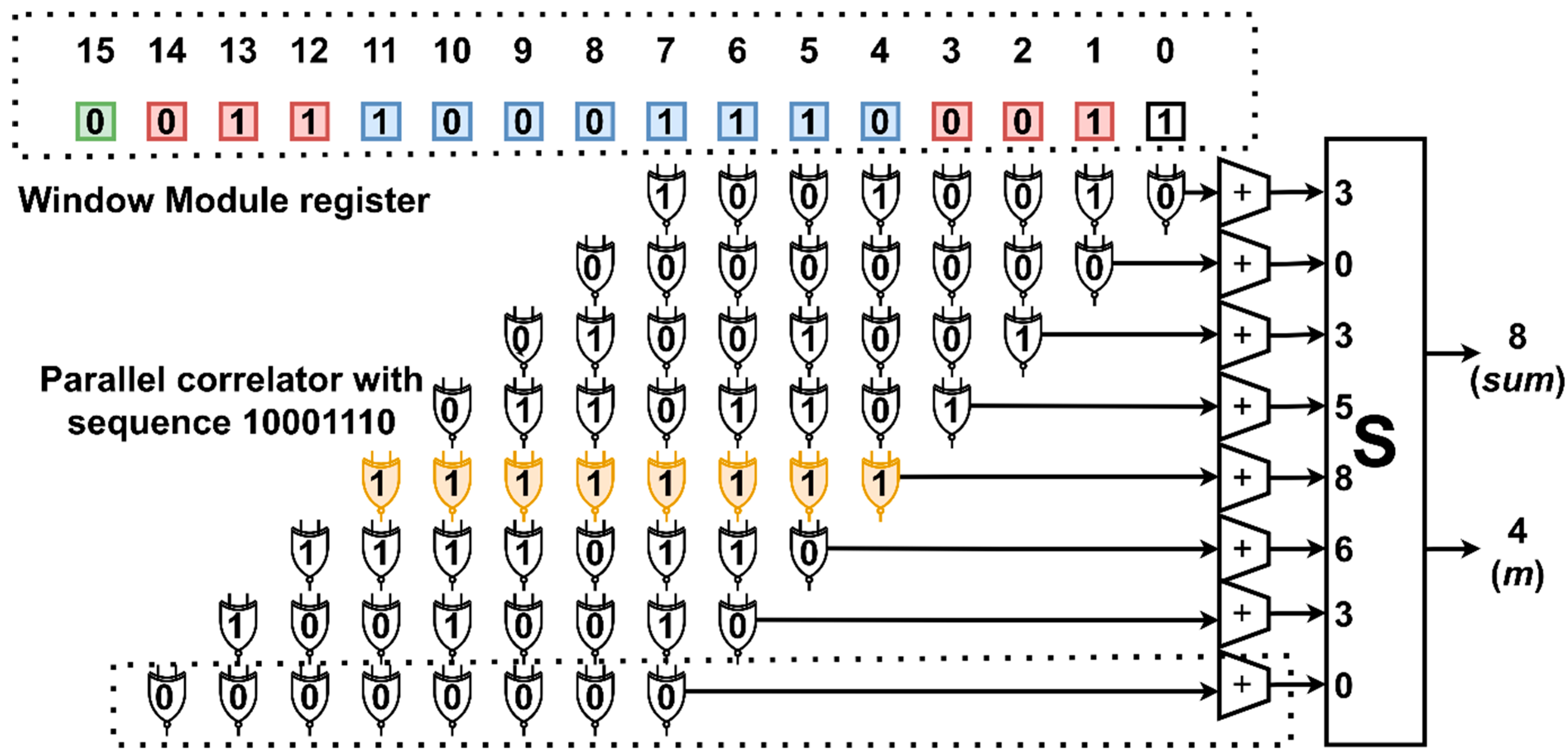
An example of the functionality and circuitry of the Window Module together with the Parallel Adder Trees and the Selector when l = 8 (length of bl) and k = 3 (length of ak, ck) can be seen in Figure 5. These lengths, although short, can clearly demonstrate how the frame synchronization process is executed. In the specific example, the sequence being searched (bl) is 10001110. For the larger l size, the circuit depicted is identical. The only difference is a larger window register and more correlators.
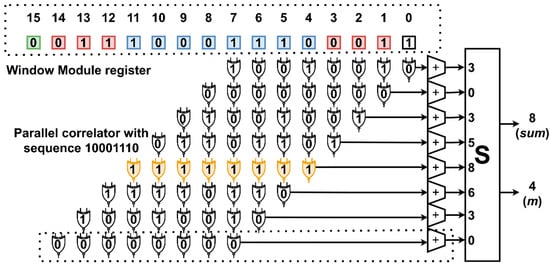
Figure 5.
Parallel correlation with window register. The numbered blocks on top represent the window module register. The “S” block is the selector circuit. The starting bit of the bl sequence (10001110) was detected on bit 4 (output m). Red squares represent sequences ak and ck (with k = 3), which are the inverted edges of bl (blue squares). The green square is the start of the payload.
The parallel input of l = 8 bits first enters the left half (15 down to 8) of the Window Module on cycle t. On cycle t + 1, the next input enters the left half, and the previous input migrates to position 7 down to 0, which brings the start of bl to position 4 of the overall register (was previously in the 12th element). This is the cycle depicted in Figure 5. For subsequent clock cycles, the elements inside the window register enter the correlation module. They are correlated with the stored sequence bl according to (2). Each line of xnor gates together with the adder tree, and at the end constitutes a correlator. There are 8 correlators. The correlation module produces the maximum value summ along with its position m at any given time. Position m represents the starting bit of bl, and it is what the Payload Capture Module utilizes to capture the payload from the incoming frame. In Figure 5, m = 4, which means that the starting bit of the payload is l + k + m = 8 + 3 + 4 = 15 (green square). The latency of the correlation module is ceil(log2l)+ ceil(log2l) = 2 × ceil(log2l) (Selector and adder tree). We notice that the only correlation value that reaches 8 is the value in the position of the first bit of bl (correct detection). The next two higher values, 6 and 5, appear only once each. This can be partly attributed to the existence of ak and ck, which indirectly influence the accuracy of detection.
Since the Correlation Module has a latency of 2 × ceil(log2l), the Payload Capture Module (next section) cannot use the Window Module register for payload capture as the inputs are not synchronized with the outputs. To capture the payload data effectively, the Payload Capture Module needs to be able to “see” the window register with a delay synchronized to the corresponding outputs of the Correlation Module. To do this, the Correlation Module is equipped with a delay buffer. The buffer causes a delay of 2 × ceil(log2l) clock cycles to the input and synchronizes it with the corresponding values summ and m. The delayed input, together with the two values, is given to the Payload Capture Module to enable payload capture.
3.3. Payload Capture Module
The Payload Capture Module utilizes the two outputs of the correlation module summ and m together with the delayed input to correctly deduce the position of the payload and capture the data. As mentioned in (1), when the value of the digital correlation is high, the two binary vectors are close in terms of likeness. Likewise, if the value of summ (which is the highest of all positions) is above a certain threshold, then this means that the correlator has located a vector at position m that is very close to bl. If the threshold is appropriately set, the Payload Capture Module can not only detect the payload but also capture it regardless of frame size. For this reason, selecting the proper value for the threshold is instrumental for the correct operation of the receiver. In general, this is achieved by experimenting. The threshold must be low enough to detect the sync word even in the presence of a lot of bit errors but not so low as to be triggered by random data frequently.
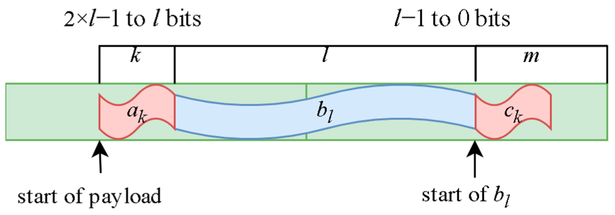
To determine the starting position of bl and the payload, the module uses a simple control unit that constantly checks the output summ of the Correlation Module. When the output surpasses the threshold at clock cycle t the control unit is activated. It assumes that the payload is found at l + k + mt and begins its capture. In the next cycle t + 1, it compares the new value of with the previous . If then the first bit of bl was at position mt and no changes are necessary. If the opposite is true, the first bit of bl is at position mt+1, and the frame capture process must restart to capture the correct bits. The position of the payload in relation to the frame header can be seen in Figure 6.

Figure 6.
Position of payload in relation to the frame header akblck.
There are multiple ways in which capture can be achieved, but in this article, we propose the simplest. If we examine Figure 6, we conclude that because bl is l bits long, l + k + mt (or l + k + mt+1) will either be outside the register or inside the left half (2 × l − 1 down to l). If it is inside the register, the capture process begins immediately. If it is not, the control unit waits one cycle to start the process. Assuming that the size of the payload is a multiple of l(p = n × l), the payload can be captured in n + 1 cycles in the following manner. When the first bit of the payload enters the left half of the register, the unit captures the last l − (k + mt) (or mt+1) bits of the register (left half), which are the first bits of the payload. For the next n − 1 cycles, all bits in the left half are captured. In the final cycle, the first k + mt (or mt+1) bits of the left half are captured. If we add all the bits together, we have l − (k + mt) + (n − 1) × l + k + mt = n × l bits, which is the entire payload. The payload is captured at the same rate as it enters the circuit, and the two-bit signal valid out is used to indicate that the capture process is underway. The biggest advantage of using this method to capture the frames is that no matter how large n is (the size of the frame), the size of the circuit does not change, only the cycles needed to capture it. While the payload capture is in progress, the correlation module is deactivated to conserve energy.
4. Implementation, Testing, and Assessment
The receiver was implemented (out of context) on the low-cost NEXYS 4 DDR FPGA board. The architecture was implemented for five settings. These were l = 123, k = 23, th = 93 (threshold); l = 112, k = 21, th = 84; l = 99, k = 17, th = 76; l = 89, k = 19, th = 70; l = 75, k = 16, th = 55. A maximum operating frequency of 125 Mhz was achieved for all cases. The bit rates were obtained by multiplying the parallel input with the operating frequency, and we have 123 bits × 125 MHz = 15.37 Gbps, 112 bits × 125 MHz = 14.00 Gbps, 99 bits × 125 MHz = 12.375 Gbps, 89 bits × 125 MHz = 11.125 Gbps, and 75 bits × 125 MHz = 9.375 Gbps. The needed hardware resources, utilization, power consumption, and bit rate are all presented in Table 1. The architecture does not consume DSP units because it only uses short-length adders, comparators, xnor gates, and registers.

Table 1.
Implementation results. LUTs and FlipFlops are standard resources for FPGAs.
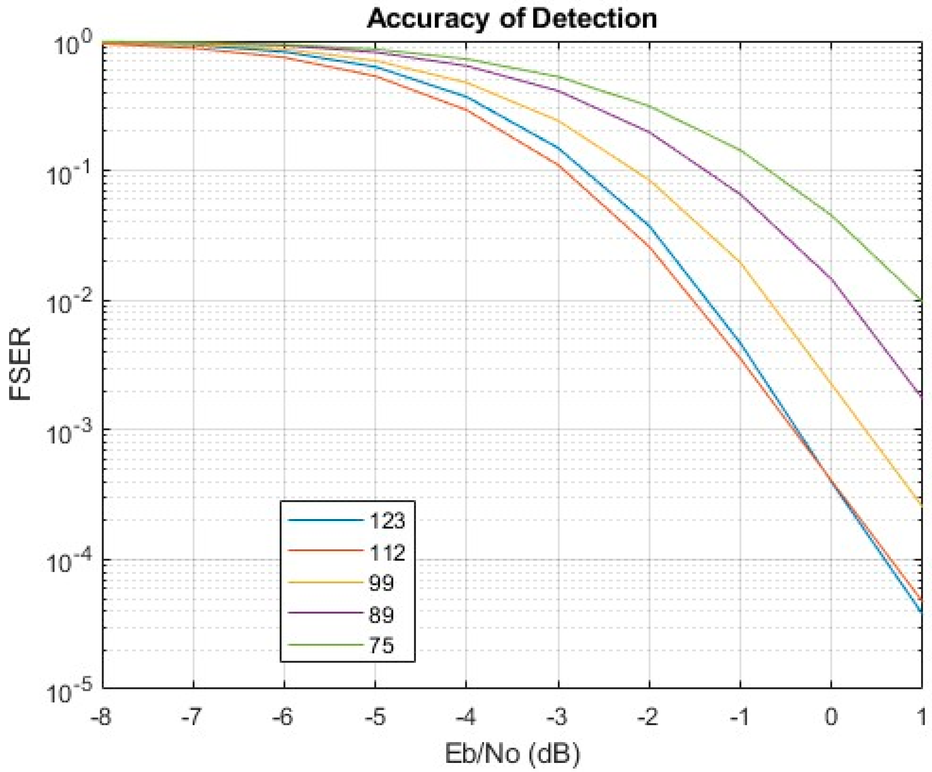
VIVADO and MATLAB were used for testing. Input bitstreams were prepared in MATLAB and inserted in the VHDL testbench as txt files. The modulation scheme of choice was 16QAM, and the range of SNR was [−8, 1]. Inputs were prepared for each SNR integer value separately (for all cases). They consisted of 21,368 frames of the form payloadjakblck (as described in Section II). The bitstreams were created, modulated with 16QAM, and driven through the AWGN channel. For every SNR value, a different preamble was used. After this process, the bitstreams were demodulated, recorded in txt files, and given as input to the implemented circuit. The implemented design outputs the payload of each frame. The captured payloads were of size 12,300 (multiple of 123), were recorded in txt files, and checked by MATLAB. The frame synchronization error rate (FSER) can be seen in Figure 7.
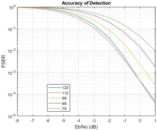
Figure 7.
Frame synchronization Error Rate of the architecture.
Since no additional processing was applied to the signal (only modulation/demodulation), the raw bit error rate for each SNR value is known by theory and can be calculated with MATLAB functions such as berawgn or qammod/qamdemod. For SNR values of interest, −1, 0, and 1, the respective BER values are 0.1637, 0.1410, and 0.1190. This applies to all different versions of the architecture because the same scheme (16QAM) was used for all of them. The difference in accuracy occurs because of the different bl lengths. Deriving an expression for FSER is also possible since the raw bit error rate (16QAM on the AWGN channel) can be directly calculated. However, even if this is the case, the random nature of bl as a binary sequence makes the mathematical calculation of FSER extremely difficult. This can and will probably be explored in future publications. For now, if bl is randomly generated, the only available data will come from testing.
We see that the implemented circuit achieves a frame synchronization error rate of 3.9311 × 10⁻⁴, 4.0247 × 10⁻⁴, 0.0022, 0.0145, 0.045 (l = 123,112,99,89,75, respectively) for 0 dB SNR on the input. This means that it misses this portion of frames at that noise level. The percentage of missed frames becomes 3.7439 × 10⁻⁵, 4.6799 × 10⁻⁵, 2.5271 × 10⁻⁴, 0.0017, 0.0097 at 1 dB SNR. It is understandable that, in general, as the size of the sync word decreases, so does the accuracy. The l = 75 implementation has significantly worse detection capability than the l = 123 version; l = 112 seems to be better at earlier SNRs, but eventually, l = 123 surpasses it. This may be an indication that k needs to be larger than 23 for l = 123. If we use SNR = 0 and 1 dB (for the AWGN channel) as the basis of comparison, we can compare our accuracy results with other methods and see how the architecture performs.
In the comprehensive study presented in [5], the authors use multiple frames embedded with sync words of a specific size to perform synchronization for different modulations. From the results reported, we see that at SNR = 0 dB, the accuracy reported is around 0.98 to 0.99 for most schemes (judging from the figures) tested with BPSK and QPSK (which are lower-order modulations than 16QAM). This is a very good result considering the fact the scheme uses Barker sequences [1]. In [6], the authors propose an advanced sequential algorithm based on likelihood metrics which offers very good synchronization. In the article, the authors test different configurations while trying to balance between the probability of detection and false detection (emulation). It is reported that at SNR = 0 dB, the probability of detection is between 0.94 and 1, and the probability of false detection is between 0 and 0.004, but because the best value for detection coincides with the worst for false detection and vice versa, the scheme never surpasses our rate (which includes false detection). The sync words used are of sizes 24 and 32, which is still far lower than what the proposed architecture can offer. Refs. [7,9] are frame synchronization schemes that belong to a different family of frame synchronization called LDPC joint frame synchronization, where LDPC error codes are used to assist the process. They offer a very detailed performance comparison between different sync word methods and the joint synchronization method. In both cases, the sync word methods seem to be better at lower SNRs but worse at higher SNRs. In all cases, however, the proposed architecture is better in terms of accuracy. In [7], at around SNR = 1 dB, the best-reported result is around 10−4 with sync word length up to 78 bits. In [9], the best-reported result (for both joint and sync word methods) is around 10−2 for SNR = 0 dB with sync word length up to 35 bits. Both use BPSK modulation. Notice that the proposed architecture needs longer sync words to reach 10−4 FSER, but this is to be expected since the sync words used are not optimally constructed, and the method of pure correlation is not optimal. All the above sync word methods are theoretical and do not offer implementation results. Ref. [9] only presents the implementation results of the LDPC joint frame synchronization method.
In terms of practical application, there are no other implementations of the method. For this reason, we have opted to compare the circuit with other circuits that are proven to be used for frame synchronization, such as LDPC decoders [10]. The proposed architecture is much easier to implement, offers higher bit rates, and consumes much less power than methods that have been proposed in recent years, such as the joint frame synchronization with LDPC. More specifically, according to the comprehensive LDPC decoder survey presented in [11], we can see that current LDPC decoder architectures, even when implemented on superior platforms such as ASIC, achieve lesser performance. Refs. [12,13] consume power of 0.164 W and 0.274 W to offer bit rates of 136 Mbps and 124.6 Mbps, respectively. Ref. [14] requires 212.4 W for 2.267 Gbps, which is drastically more power for far less speed. This is brought even more into perspective when we see that, in general, implementations on FPGA fabric consume more power and run slower than implementations on ASIC, as reported in [15]. Decoding LDPC codes also has much higher complexity (in terms of cycles) than digital correlation [16], which is likely to slow down the process even further. Thus, it would be more efficient to consider the use of the proposed architecture to synchronize the frame and then use the LDPC purely for error correction.
Moreover, the architecture possesses some extra merits which are tied to its minimalist design. It can capture any size of payload without changing size. It can be used as a security mechanism to mask transmission on the physical layer [17] because the sync word sequence bl is random. It can also be implemented on very low-cost platforms, which makes it suitable for applications with strict resource constraints, such as IoT [18]. Finally, the architecture itself can be used in multiple ways. For example, one can send in alignment frames first and then data frames or start sending data frames immediately. The architecture can provide the position of the frame along with the payload, so it can be used either way. It is also not influenced by previous detections. The only thing it guarantees is the probability of missing a frame under a certain SNR. The question of what the optimal strategy is to follow when using this architecture (use alignment frames first, calculate position, and then send data frames or just send data frames from the start), in terms of overall effective throughput, warrants further investigation and will be the subject of future work.
5. Conclusions
In this paper, we have presented a simple yet accurate novel frame synchronization architecture based on the sync word correlation method. The architecture uses very long sync words, which are placed in front of the payload to detect and capture it. It can be implemented on very low-cost platforms (NEXYS 4 DDR FPGA board) and consumes little in terms of hardware and power while providing bit rates of up to 15.375 Gbps. It offers very high synchronization accuracy even at low SNRs. Future work involves modified versions aimed at maximizing specific traits such as accuracy, bit rate, security, and power efficiency.
Funding
This research received no external funding.
Informed Consent Statement
Not applicable.
Data Availability Statement
Data are contained within the article.
Conflicts of Interest
The author declares no conflicts of interest.
References
- Barker, R.H. Group Synchronization of Binary Digital Systems. In Communication Theory; Academic Press: Cambridge, MA, USA, 1953; pp. 273–287. [Google Scholar]
- Bekar, M.; Baker, C.J.; Hoare, E.G.; Gashinova, M. Joint MIMO Radar and Communication System Using a PSK-LFM Waveform With TDM and CDM Approaches. IEEE Sens. J. 2021, 21, 6115–6124. [Google Scholar] [CrossRef]
- Massey, J. Optimum Frame Synchronization. IEEE Trans. Commun. 1972, 20, 115–119. [Google Scholar] [CrossRef]
- Nielsen, P. Some Optimum and Suboptimum Frame Synchronizers for Binary Data in Gaussian Noise. IEEE Trans. Commun. 1973, 21, 770–772. [Google Scholar] [CrossRef]
- Bastaki, E.M.; Tan, H.H.; Shi, Y.; Letaief, K.B. Frame Synchronization Based on Multiple Frame Observations. IEEE Trans. Wirel. Commun. 2010, 9, 1097–1107. [Google Scholar] [CrossRef]
- Chiani, M.; Martini, M.G. On Sequential Frame Synchronization in AWGN Channels. IEEE Trans. Commun. 2006, 54, 339–348. [Google Scholar] [CrossRef]
- Lee, D.-U.P.A.U.; Kim, H.; Jones, C.R.; Villasenor, J.D. Pilotless Frame Synchronization for LDPC-Coded Transmission Systems. IEEE Trans. Signal Process. 2008, 56, 2865–2874. [Google Scholar] [CrossRef]
- Matsuyuki, S.; Tsuneda, A. A Study on Aperiodic Auto-Correlation Properties of Concatenated Codes by Barker Sequences and NFSR Sequences. In Proceedings of the 2018 International Conference on Information and Communication Technology Convergence (ICTC), Jeju, Republic of Korea, 17–19 October 2018; pp. 664–666. [Google Scholar] [CrossRef]
- Ding, X.; Zhou, K.; Li, G.; Yang, K.; Gao, X.; Yuan, J.; An, J. Customized Joint Blind Frame Synchronization and Decoding Methods for Analog LDPC Decoder. IEEE Trans. Commun. 2024, 72, 756–770. [Google Scholar] [CrossRef]
- Feng, Z.; Xu, M.; Xiao, L.; Zhang, Z.; Zhou, J.; Jiang, T. LDPC Assisted Blind Frame Synchronization: Efficient Measurement Mechanism and Low-Complexity Algorithm. In Proceedings of the 2021 7th International Conference on Computer and Communications (ICCC), Chengdu, China, 10–13 December 2021; pp. 355–359. [Google Scholar] [CrossRef]
- Ferraz, O.; Subramaniyan, S.; Chinthalaa, R.; Andrade, J.; Cavallaro, J.R.; Nandy, S.K.; Silva, V.; Zhang, X.; Purnaprajna, M.; Falcao, G. A Survey on High-Throughput Non-Binary LDPC Decoders: ASIC, FPGA, and GPU Architectures. IEEE Commun. Surv. Tutor. 2022, 24, 524–556. [Google Scholar] [CrossRef]
- Song, S.; Cui, H.; Tian, J.; Lin, J.; Wang, Z. A Novel Iterative Reliability-Based Majority-Logic Decoder for NB-LDPC Codes. IEEE Trans. Circuits Syst. II Express Briefs 2020, 67, 1399–1403. [Google Scholar] [CrossRef]
- Ueng, Y.-L.; Liao, K.-H.; Chou, H.-C.; Yang, C.-J. A High-Throughput Trellis-Based Layered Decoding Architecture for Non-Binary LDPC Codes Using Max-Log-QSPA. IEEE Trans. Signal Process. 2013, 61, 2940–2951. [Google Scholar] [CrossRef]
- Toriyama, Y.; Markovic, D. A 2.267-Gb/s, 93.7-pJ/bit Non-Binary LDPC Decoder With Logarithmic Quantization and Dual-Decoding Algorithm Scheme for Storage Applications. IEEE J. Solid-State Circuits 2018, 53, 2378–2388. [Google Scholar] [CrossRef]
- Boutros, A.; Betz, V. FPGA Architecture: Principles and Progression. IEEE Circuits Syst. Mag. 2021, 21, 4–29. [Google Scholar] [CrossRef]
- Imad, R.; Sicot, G.; Houcke, S. Blind Frame Synchronization for Error Correcting Codes Having a Sparse Parity Check Matrix. IEEE Trans. Commun. 2009, 57, 1574–1577. [Google Scholar] [CrossRef]
- Zhang, C.; Yue, J.; Jiao, L.; Shi, J.; Wang, S. A Novel Physical Layer Encryption Algorithm for LoRa. IEEE Commun. Lett. 2021, 25, 2512–2516. [Google Scholar] [CrossRef]
- Migabo, E.M.; Djouani, K.D.; Kurien, A.M. The Narrowband Internet of Things (NB-IoT) Resources Management Performance State of Art, Challenges, and Opportunities. IEEE Access 2020, 8, 97658–97675. [Google Scholar] [CrossRef]


Disclaimer/Publisher’s Note: The statements, opinions and data contained in all publications are solely those of the individual author(s) and contributor(s) and not of MDPI and/or the editor(s). MDPI and/or the editor(s) disclaim responsibility for any injury to people or property resulting from any ideas, methods, instructions or products referred to in the content. |
© 2024 by the author. Licensee MDPI, Basel, Switzerland. This article is an open access article distributed under the terms and conditions of the Creative Commons Attribution (CC BY) license (https://creativecommons.org/licenses/by/4.0/).