Article

Research on a New Inverter Control Strategy of Induction Heating Power Supply

1
School of Electrical & Information Engineering, Hubei University of Automotive Technology, Shiyan 442002, China
2
School of Electrical Engineering and Automation, Wuhan University, Wuhan 430079, China
*
Author to whom correspondence should be addressed.
Electronics 2024, 13(17), 3469; https://doi.org/10.3390/electronics13173469
Submission received: 2 July 2024 / Revised: 19 August 2024 / Accepted: 23 August 2024 / Published: 31 August 2024
(This article belongs to the Special Issue Advances in Power Conversion Architectures)

Abstract

:
To achieve “high voltage, low current” in the induction heating power circuit, enhance the flexibility of component selection in the circuit, and improve the quality of the inverter’s output waveform, a new control strategy of a single-phase NPC three-level inverter with unipolar frequency-doubling SPWM method is proposed. With the series connection of IGBTs in a single-phase NPC three-level inverter, the voltage withstand requirement of IGBT is reduced by half. The middle four IGBTs are controlled using unipolar frequency-doubling SPWM, while the outer four IGBTs are turned on later and turned off earlier to address the neutral point voltage imbalance issue in the inverter. Simulation results show that, compared with the traditional bipolar SPWM-controlled single-phase full-bridge inverter, the DC-side input voltage of the inverter can be double, and the current flowing through the entire circuit can be halved under the same output power using the proposed method.

1. Introduction

With the adjustment of the national energy structure and the development of power electronics technology, induction heating power supplies have been widely used in many fields due to their precise temperature control, fast heating speed, and high energy utilization rate [1,2,3,4]. As a key part of the induction heating power supply, the circuit structure and control strategy of the inverter circuit have always been a research focus. Li Sen et al. proposed a bipolar SPWM as the control strategy for the induction heating power inverter circuit [5]. Its inverter circuit has a simple topology, and the control strategy and implementation methods are relatively mature. However, the entire circuit cannot achieve “high voltage, low current” due to the limitations of the IGBT. Lu Hua et al. used a tapped transformer coupling method to make the load operating frequency twice that of the IGBT operating frequency [6], but this requires many parameters to be calculated, and the transformer is relatively bulky. Wang Ai et al. proposed the parallel application of IGBTs for high power, which increases the current flowing through the main circuit and improves the circuit’s output power, but it is not conducive to component selection in the circuit [7]. In high-power inverter power supplies, because the current flowing through the IGBT can reach hundreds of amps, the selected IGBT capacity is relatively large. As a result, the switching frequency of the IGBT cannot be too high during modulation [8], and this results in more harmonics in the output waveform and poor output waveform quality.
This paper proposes a new control strategy for induction heating power supplies by combining a single-phase NPC three-level inverter circuit with unipolar frequency-doubling SPWM. The use of the single-phase NPC three-level inverter circuit reduces the voltage withstand requirement of the IGBT, increases the DC-side input voltage, and achieves “high voltage, low current”. The middle four IGBTs are controlled using unipolar frequency-doubling SPWM, and the outer four IGBTs are turned on later and turned off earlier, which not only reduces the harmonic content of the inverter output waveform but also avoids the neutral point voltage imbalance issue brought by the single-phase NPC three-level inverter, making the single-phase NPC three-level inverter circuit suitable for the generation of low-frequency sinusoidal wave inversion.

2. Technical Specifications

According to the actual project requirements, the technical parameters of the new inverter circuit are shown in Table 1.
The inductance of the custom-made induction heating coil in the project was measured as 1.4 mH, and the resistance R was 0.1 Ω using an LCR meter.

3. New Inverter Control Strategy

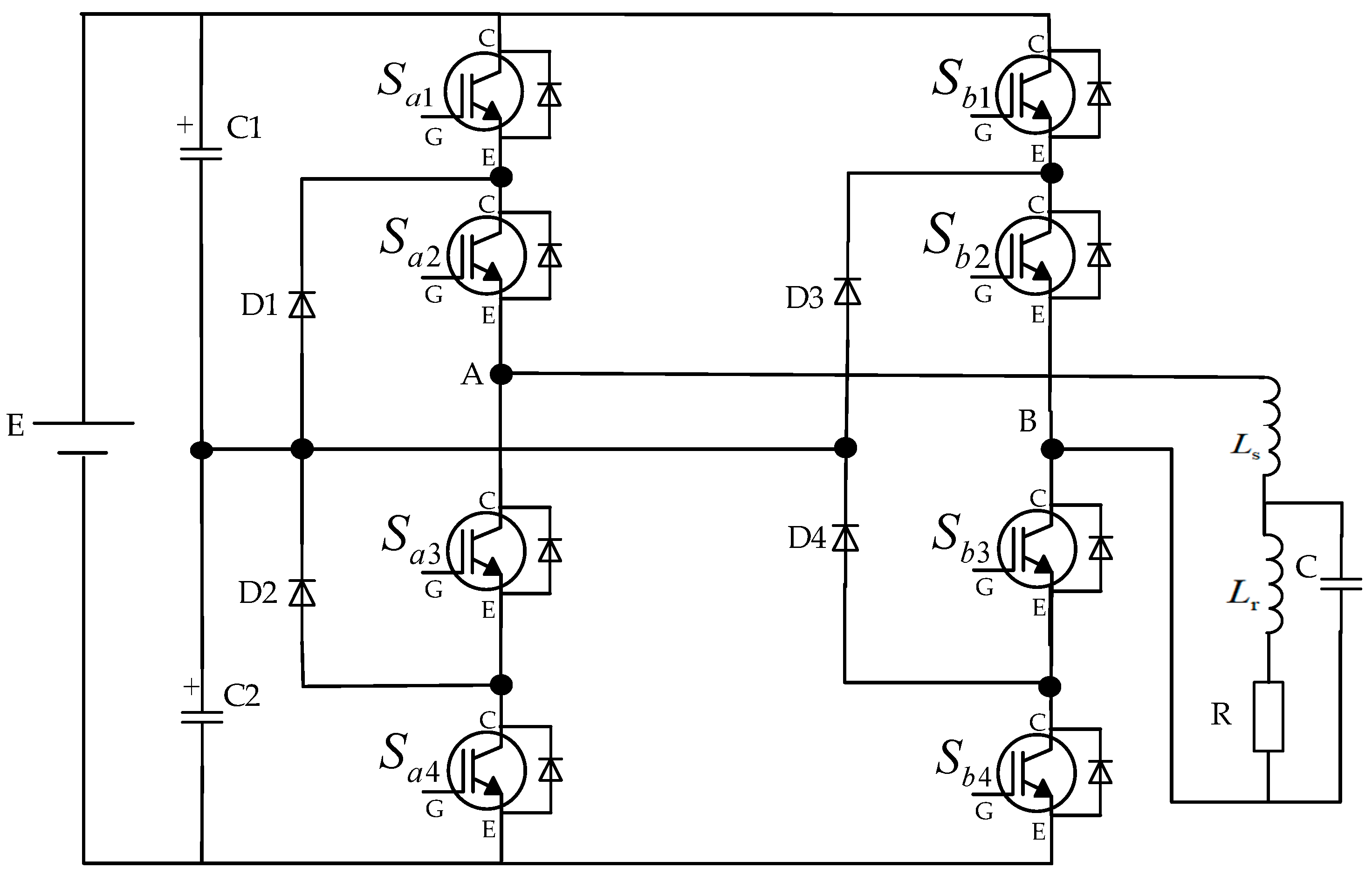
3.1. Circuit Structure

The topology of the single-phase NPC three-level inverter circuit is shown in Figure 1. It mainly consists of a DC power supply (E), two DC-side large capacitors with the same parameters (C1, C2), two bridge arms (a, b), a compensation inductor (Ls), a compensation capacitor (C), and an induction heating coil (R, Lr). Each bridge arm consists of four IGBT switches and two clamping diodes, with point O as the neutral point voltage reference. Due to the series connection of IGBTs, the maximum voltage of each IGBT withstands E/2. When using IGBTs of the same specifications and outputting the same power in the inverter, the DC-side input voltage of the single-phase NPC three-level inverter circuit can be twice that of the single-phase full-bridge inverter circuit, reducing the current flowing through the entire circuit by half, achieving “high voltage, low current” in the entire circuit, increasing the flexibility of component selection in the circuit, and reducing the loss of useless power in the circuit.

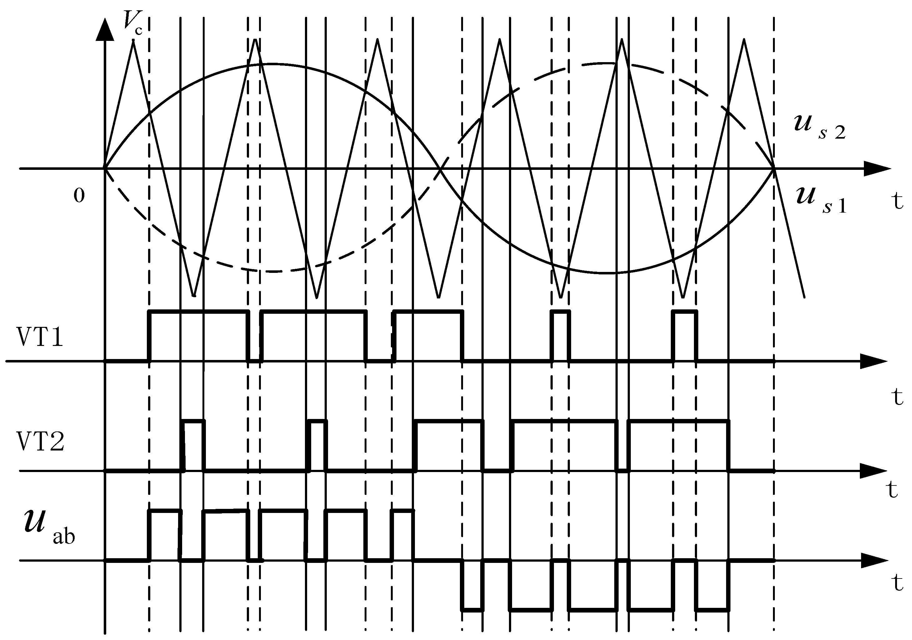
3.2. Unipolar Frequency-Doubling SPWM Modulation Principle

Unipolar frequency-doubling SPWM controls the two-phase bridge arms separately. Figure 2 shows the modulation principle of unipolar frequency-doubling SPWM, and Figure 3 shows the single-phase full-bridge inverter topology. The sine wave is compared with the triangular carrier wave in the A-phase bridge arm. When the sine wave is greater than the triangular wave, VT1 is turned on; otherwise, VT4 is turned on. The B-phase bridge arm compares the inverse sine wave with the same triangular carrier wave. When the inverse sine wave is greater than the triangular wave, VT2 is turned on; otherwise, VT3 is turned on [9]. As shown in Figure 2, in one carrier cycle, each IGBT in the single-phase full-bridge inverter (Figure 3) switches once but the output voltage level changes twice, meaning that the output voltage frequency is twice the carrier frequency. The switching frequency of the IGBT modulated by unipolar frequency-doubling SPWM is only half that of other modulation methods but can output voltage square waves of the same frequency [10].
The higher the IGBT switching frequency, the higher the heat generated during its on–off operations and the higher the IGBT loss [11]. As described in [12], the relationship between switching loss and switching frequency is given as follows:
P s = f s × ( P o n + P o f f )
where Ps represents the IGBT switching loss; fs is the IGBT switching frequency; Pon is the IGBT turn-on loss; and Poff is the IGBT turn-off loss.
P o n = 1 t o n 0 t o n u i d t P o f f = 1 t o f f 0 t o f f u i d t
where u represents the instantaneous value of the collector–emitter voltage; i represents the instantaneous value of the collector current; ton represents the duration of the turn-on process; and toff represents the duration of the turn-off process.
From Equations (1) and (2), compared with the traditional bipolar SPWM-controlled full-bridge inverter under the same conditions of power loss and output power, the new control strategy combining unipolar frequency-doubling SPWM of the single-phase NPC three-level inverter doubles the switching frequency and enhances the output voltage frequency fourfold. According to the literature [13], the harmonic distribution of the inverter’s output voltage is concentrated around integer multiples of the carrier frequency. Increasing the carrier frequency shifts the harmonic distribution to higher frequency bands, simplifies the filtering part and improves the quality of the inverter output waveform. According to the area equivalence principle and integration principle, the higher the output voltage frequency, the more PWM square waves, and the better the quality of the output sine wave [14].

3.3. Circuit Operating Principle

The working waveforms of unipolar frequency-doubling SPWM are shown in Figure 4a. In the figure, us1 and us2 are a pair of inverse sine modulation waves, and Vc is the triangular carrier wave. us1 and us2 are compared to Vc, respectively, and generate two independent PWM pulses pwmA and pwmB. When us1 is greater than Vc, the pulse signal pwmA is at a high level; otherwise, it is at a low level. When us2 is greater than Vc, the pulse signal pwmB is at a high level; otherwise, it is at a low level. The falling edges of the two pulse signals pwmA and pwmB are delayed by 2us to obtain the signals pwmA1 and pwmB1. The rising edges of the two pulse signals pwmA and pwmB are delayed by 2 us to obtain the signals pwmA2 and pwmB2. Figure 4b shows the circuit diagram of the pulse signals driving the switching transistors.
The logical relationship between the eight switching transistors shown in Figure 4b and the four pulse signals pwmA1, pwmB1, pwmA2, pwmB2.
S a 2 = pwmA 1 , S a 3 = pwmA 1 ¯ S b 2 = pwmB 1 , S b 3 = pwmB 1 ¯ S a 1 = pwmA 2 , S a 4 = pwmA 2 ¯ S b 1 = pwmB 2 , S b 4 = pwmB 2 ¯
Compared with traditional methods, such as the SPWM control method [15], specific harmonic elimination method [16], and the space vector control method [17,18,19], the unipolar frequency-doubling SPWM method solves the problem of increased power loss in the generation of low-frequency sine waves and is easy to implement. In traditional methods, the neutral point voltage imbalance is caused by the inverter’s output voltage being half the bus voltage for a long time, which leads to the neutral point voltage imbalance in the DC-side capacitors [20]. In the new control method, to ensure that the middle four IGBTs in the single-phase NPC three-level inverter turn on earlier than the outer four IGBTs, the inverter output voltage contains an E/2 level, and the time of existence of the E/2 level is particularly short, only 2 us in this paper. Therefore, there will be no energy loss and replenishment in the capacitors and the neutral point voltage remains stable. This solves the problem of neutral point voltage imbalance in the inverter, making the inverter circuit suitable for low-frequency sinusoidal wave inversion generation.

3.4. Circuit Parameter Design

Since the time of existence of the E/2 level is very short, the operating state of the inverter circuit with an output voltage of E/2 is ignored. The overall circuit operating state is similar to that of a traditional single-phase full-bridge inverter circuit. The designed circuit parameters based on Table 1 are as follows:
(1)
Selection of voltage divider capacitors
The function of the DC-side capacitors C1 and C2 is to stabilize the DC-side voltage and suppress DC-side current fluctuations. The calculation formula is:
C 1 = C 2 = ( 6 ~ 8 ) 1 f 0 2 U d 2 / ( P max / η ) = 6.315 ~ 8.421   mF
(2)
Design of compensation inductor parameters
The amplitude of the fundamental voltage at the inverter output is:
V = 4 U d π 1273   V
Under the maximum output power condition of the circuit, the ratio of the inductance Ls/Lr is:
β = V 2 R P max = 9
The value of the compensation inductor Ls is:
L s = β L r = 12.6   mH
(3)
Design of compensation capacitor parameters
According to the resonance formula, the value of the compensation capacitor C is:
L 0 = L s | | L r = L s L r L s + L r 1.26   mH
C = 1 ω 0 2 L 0 = 1 ( 2 π f 0 ) 2 L 0 = 8.041 × 10 3   uF
(4)
Selection of clamping diodes
The effective value of the AC output current of the inverter is:
I a b = P max V / 2 111   A
The reverse voltage withstand capability of the clamping diode is half of the dc bus voltage, i.e., 500 V. Considering a margin of 2~3 times, the rated voltage of the clamping diode is set to 1500 V. The forward current and the inverter output current are 111 A. Considering a margin of 2~3 times, the rated current of the clamping diode is set to 300 A.
(5)
Selection of IGBTs
The DC-side input voltage of the inverter circuit is 1000 V, and the rated output current is 111 A. Due to the series connection of two IGBTs, the voltage borne by each IGBT is approximately 500 V. When selecting power devices, the actual circuit working conditions, device surge voltage resistance, and overcurrent capability are usually considered with a margin of 2~3 times. Therefore, the selected IGBT needs to meet the requirements of a static blocking voltage of 1500 V and a current carrying capacity of 300 A.

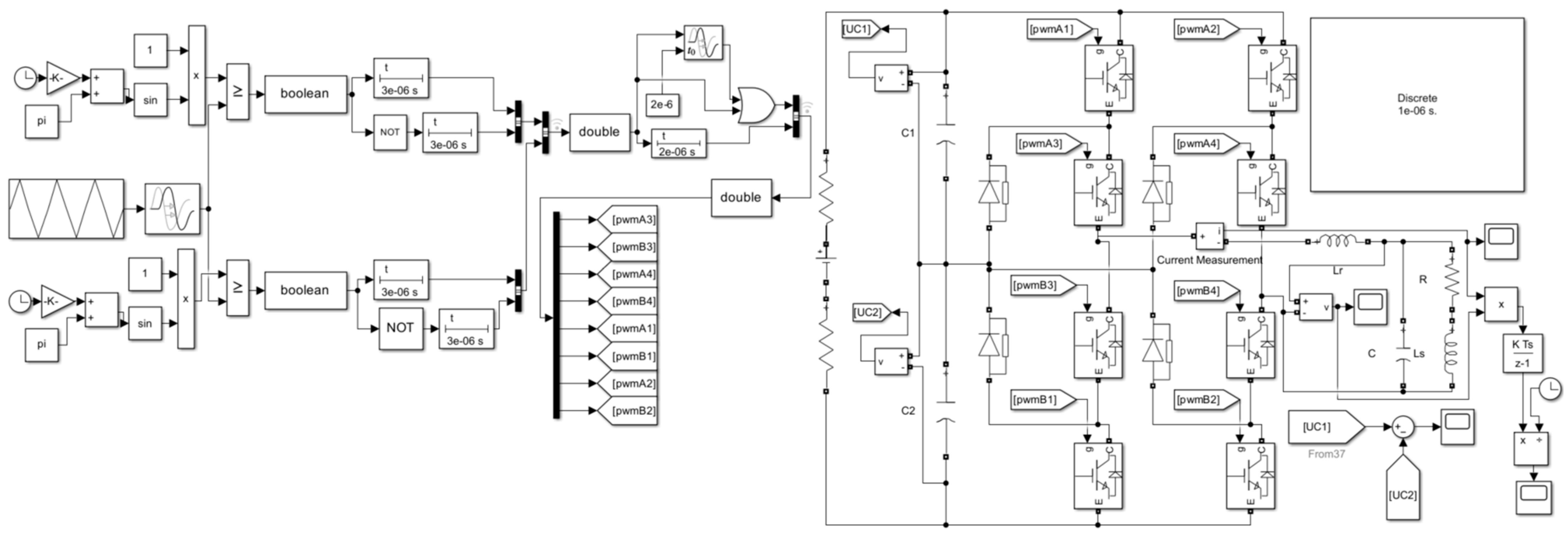
4. Simulation Verification

4.1. Simulation Setup

The simulation of the new inverter control strategy was built based on the calculated parameters. The bus voltage in Table 1 was reduced to 540 V, and the other technical parameters remained unchanged. According to the parameter selection basis of the new inverter control strategy, the simulation parameters of the traditional control strategy were designed and built. The two simulation circuits are shown in Figure 5 and Figure 6.

4.2. Simulation Comparison

(1)
The output power of the inverter with the new control strategy is shown in Figure 7. The design parameters were verified to achieve the rated output power.
(2)
The voltage difference between C1 and C2 is shown in Figure 8. As can be seen from Figure 8, the voltage difference between the two ends of the DC capacitor of the single-phase NPC three-level inverter is 0 and the midpoint potential voltage is stable, making the circuit structure suitable for low frequency sine wave generation.
(3)
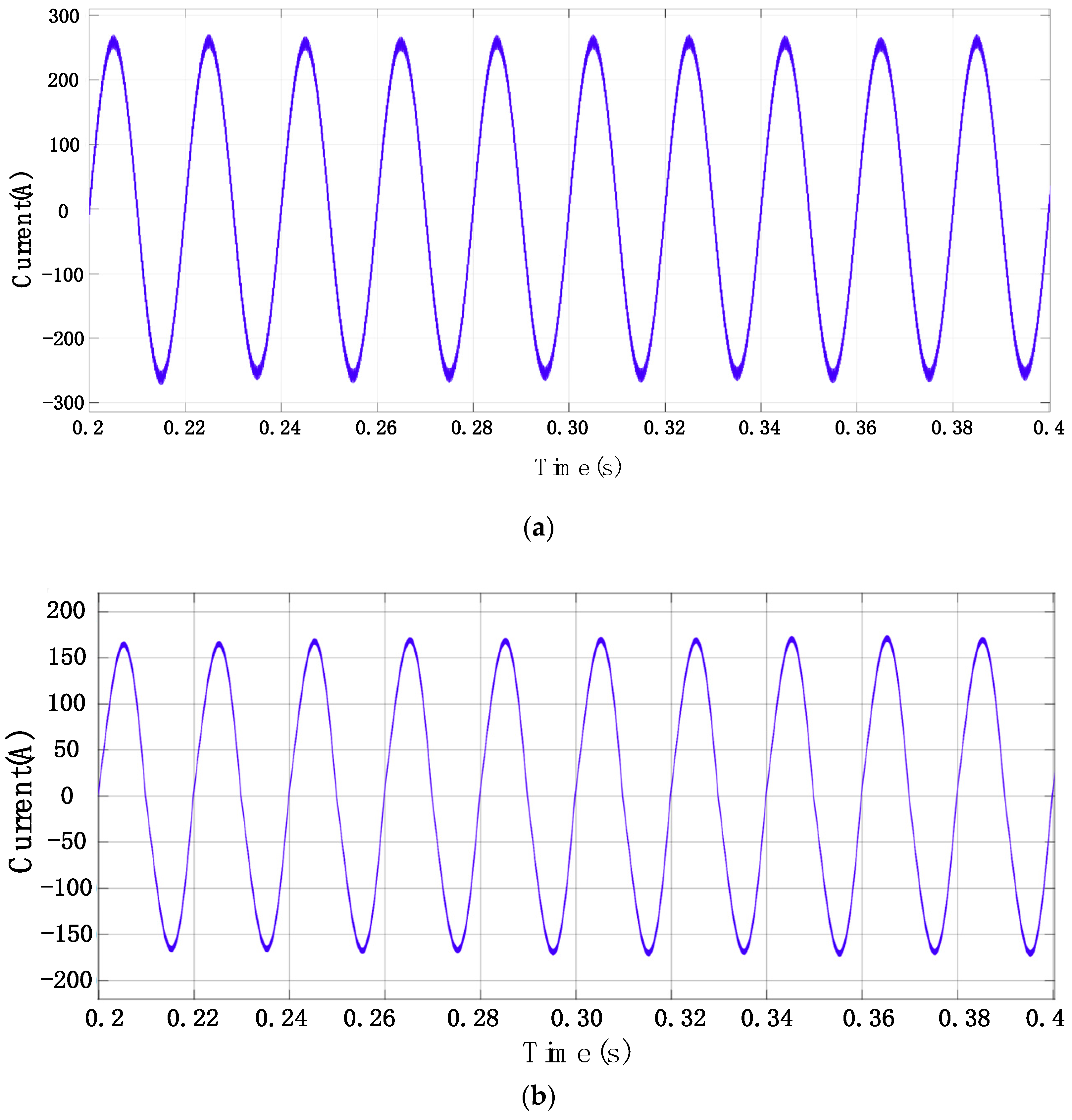
The output currents of the two inverter circuits are shown in Figure 9. The current in the single-phase NPC inverter is much smaller than that in the single-phase full-bridge inverter. Therefore, it increases the flexibility of the selection of components such as reactors, capacitors, and conductive cables that are selected based on the current in the single-phase NPC circuit.
(4)
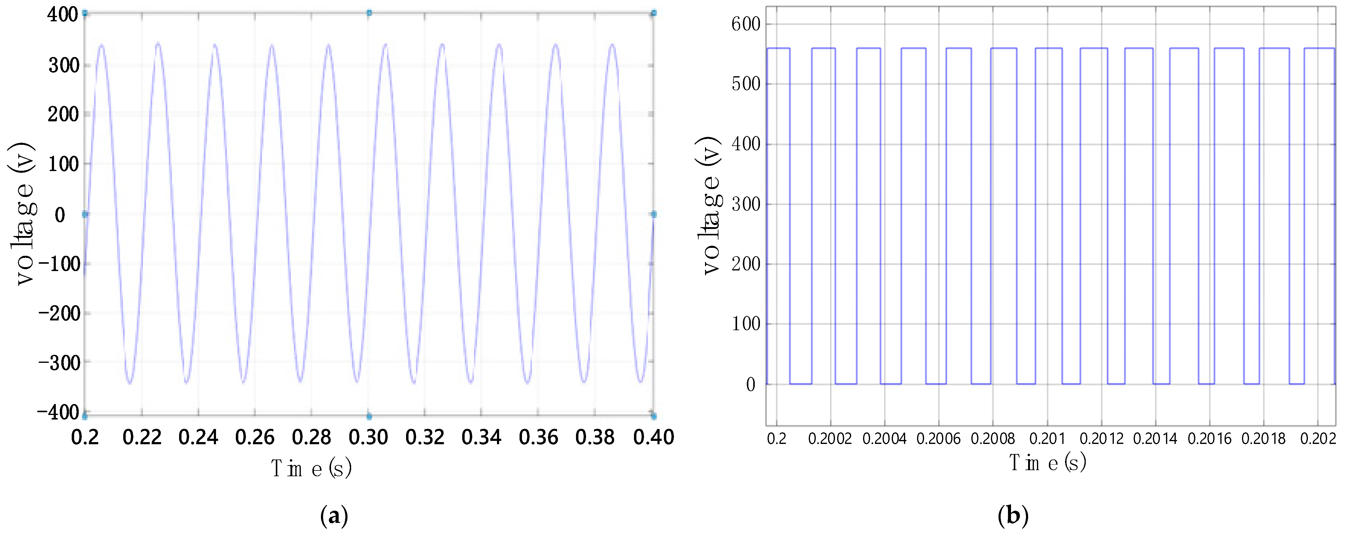
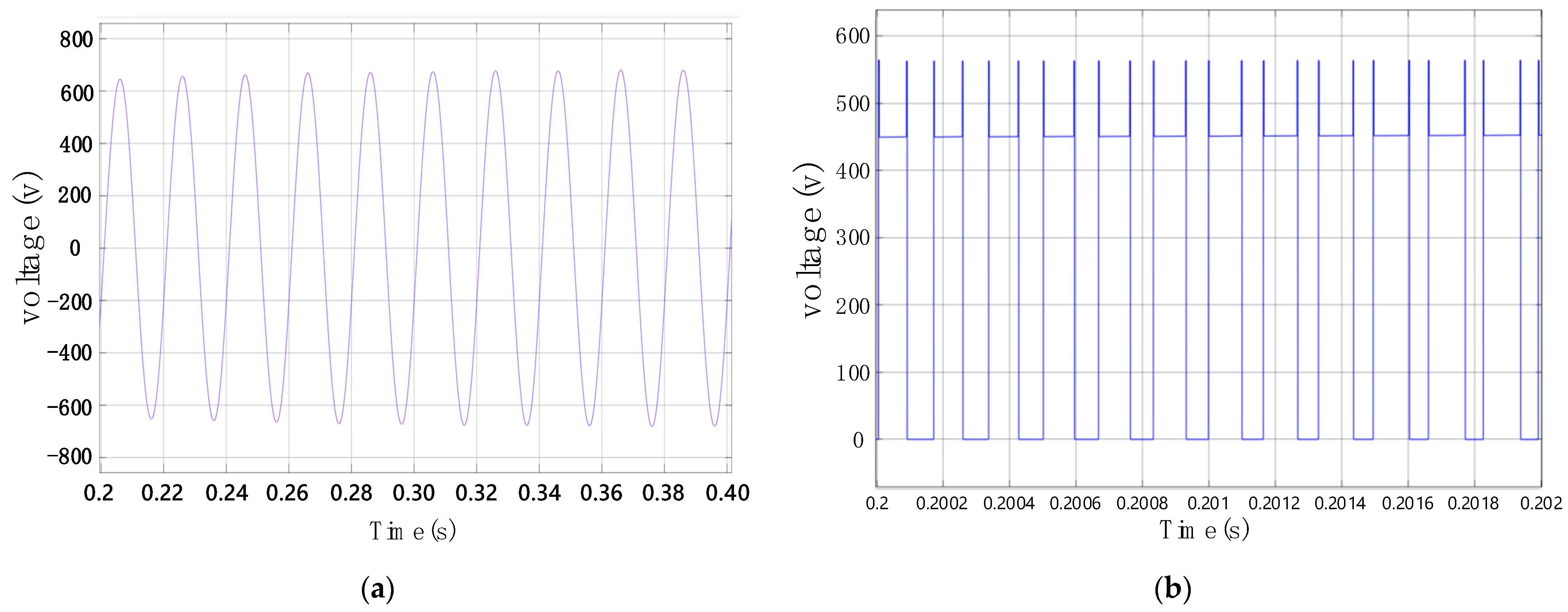
The voltages across the load and IGBTs in the two inverter circuits are shown in Figure 10 and Figure 11. It is known that the dc bus voltage of the single-phase NPC inverter circuit is 1000 V and the dc bus voltage of the single-phase full-bridge inverter is 540 V. It can be seen from the figures that when the voltages across the IGBTs in the two inverters are similar, the output voltage of the single-phase NPC inverter is nearly twice that of the single-phase full-bridge inverter, achieving the goal “high voltage, low current”.
(5)
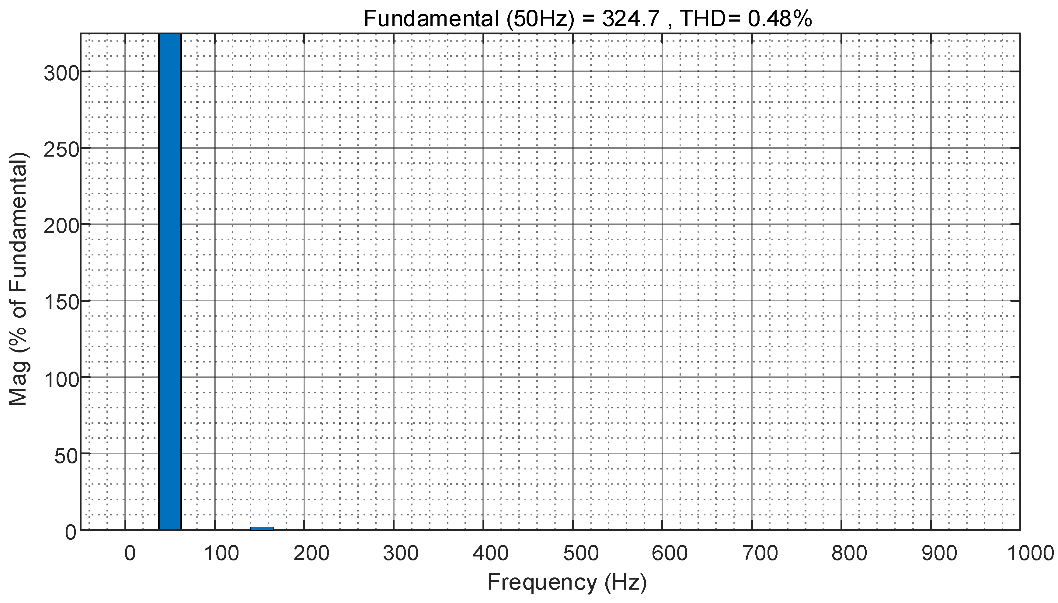
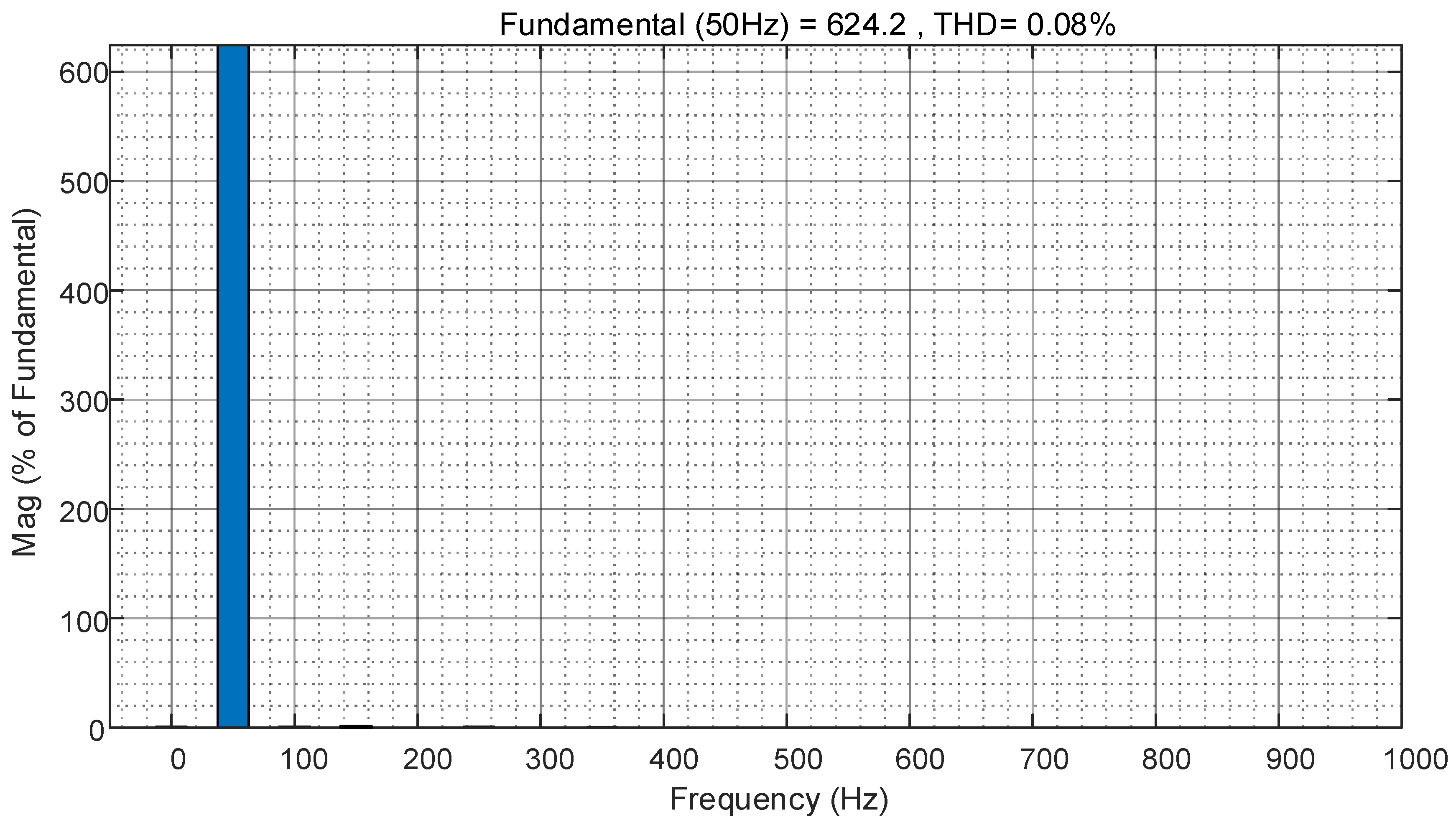
The FFT analysis of the output voltages of the two inverters is shown in Figure 12 and Figure 13. The THD value of the output voltage with the new control strategy is 0.08%, while the THD value of the output voltage with the traditional control strategy is 0.48%. There is a reduction of 0.40% for the former compared with the latter. This verifies that the new control strategy can improve the quality of the inverter’s output waveform.
The above simulation results show that, in low-frequency high-power induction heating power supplies, replacing the single-phase full-bridge inverter circuit with the single-phase NPC three-level inverter circuit reduces the voltage withstand requirement of the IGBT in the entire inverter circuit, increases the DC-side input voltage, facilitates the achievement of “high voltage, low current” in the entire circuit, and is more favorable for component selection in the circuit. Using unipolar frequency-doubling SPWM to control the single-phase NPC three-level inverter circuit can solve the problem of neutral point voltage imbalance in the single-phase NPC three-level inverter circuit, making the single-phase NPC three-level inverter circuit structure applicable to low-frequency sinusoidal wave inversion generation.

5. Conclusions

This paper proposes a new control strategy for induction heating power supplies that combines a single-phase NPC three-level inverter with unipolar frequency-doubling SPWM. It effectively realizes the circuit characteristics of “high voltage, low current”. Through series voltage division and precise timing control of IGBTs, the voltage withstand requirement of the IGBT is reduced. Furthermore, the DC bus voltage is increased and the neutral point voltage imbalance problem is solved. Simulation results show that, compared with the traditional bipolar SPWM control, the proposed strategy increases the DC bus voltage and reduces the current stress under the same output power, significantly improving the system’s efficiency and waveform quality. This research provides new ideas for the optimized design of induction heating power supplies.

Author Contributions

Conceptualization, H.H. and Y.K.; methodology, H.H.; software, Y.K.; validation, H.H., Y.K. and J.C.; formal analysis, H.H.; investigation, J.S.; resources, J.C.; data curation, W.J.; writing—original draft preparation, Y.K.; writing—review and editing, J.C.; visualization, F.S.; supervision, W.J.; project administration, S.C.; funding acquisition, H.H. All authors have read and agreed to the published version of the manuscript.

Funding

This research was funded by Technology Innovation Project of Hubei Province (2023BEB015).

Data Availability Statement

The original contributions presented in the study are included in the article, further inquiries can be directed to the corresponding author.

Conflicts of Interest

The authors declare no conflict of interest.

References

  1. Pop, O.; Taut, A. Analysis and simulation of power inverter with load variation for induction heating applications. In Proceedings of the International Spring Seminar on Electronics Technology, ISSE, Warsaw, Poland, 12–16 May 2010; pp. 378–382. [Google Scholar]
  2. Bayindir, N.S.; Kükrer, O.; Yakup, M. DSP-based PLL controlled 50–100 kHz 20 kW high frequency induction heating system for surface hardening and welding applications. IEE Proc.-Electr. Power Appl. 2003, 150, 365–371. [Google Scholar] [CrossRef]
  3. Han, W.; Chau, K.; Lam, W. All-utensil domestic induction heating system. Energy Convers. Manag. 2019, 195, 1035–1043. [Google Scholar] [CrossRef]
  4. Lucia, O.; Maussion, P.; Dede, E.J.; Burdío, J.M. Induction Heating Technology and Its Applications: Past Developments, Current Technology, and Future Challenges. IEEE Trans. Ind. Electron. 2014, 61, 2509–2520. [Google Scholar] [CrossRef]
  5. Li, S.; Huang, H.; Sun, F.; Lu, J.; Sun, Y. Design of signal source for induction heating power supply. J. Hubei Automob. Ind. Coll. 2020, 34, 63–68. [Google Scholar]
  6. Lu, H.; Hu, J.; Bi, G.; Xiang, Y. Frequency-doubled induction heating power supply based on center-tapped transformer. J. Electrotechnol. 2016, 31, 188–194. [Google Scholar]
  7. Wang, A. Design of high-power IGBT parallel power modules. Power Electron. Technol. 2022, 56, 128–131. [Google Scholar]
  8. Li, C. Research on inverter power supply system based on unipolar frequency doubling SPWM modulation. Ningxia Eng. Technol. 2009, 8, 197–200. [Google Scholar]
  9. Li, C. Research on Digital Control and Main Circuit of High Power Inverter; Xi’an University of Technology: Xi’an, China, 2009. [Google Scholar]
  10. Marko, M. Performance Analysis of High-Speed Electric Machines Supplied by PWM Inverters Based on the Harmonic Modeling Method. Energies 2021, 14, 2606. [Google Scholar] [CrossRef]
  11. Ding, X.; Du, M.; Duan, C.; Guo, H.; Xiong, R.; Xu, J.; Cheng, J.; kwong Luk, P.C. Analytical and experimental evaluation of SiC-inverter nonlinearities for traction drives used in electric vehicles. IEEE Trans. Veh. Technol. 2017, 67, 146–159. [Google Scholar] [CrossRef]
  12. Kong, W.; Liu, J.; Shao, Q.; Huang, S. Analysis of the effect of IGBT switching frequency of drive motor controller on the efficiency of drive system. Eng. Mach. 2022, 53, 21–25+8. [Google Scholar]
  13. Wang, W.; Li, K.; Liu, Z. Research on frequency doubling technique and harmonic suppression method of SPWM inverter. Micromotors 2015, 48, 60–64. [Google Scholar]
  14. Nie, X.; Huang, H.; Zhao, Y.; Lu, J. Harmonic analysis of unipolar frequency-doubled SPWM. J. Hubei Inst. Automob. Ind. 2018, 32, 65–68+74. [Google Scholar]
  15. Lee, S.J.; Lee, J.S.; Lee, B.K. Novel switching method for single-phase NPC three-level inverter with neutral-point voltage control. Int. J. Electron. 2017, 105, 303–323. [Google Scholar] [CrossRef]
  16. Li, L.; Czarkowski, D.; Liu, Y.; Pillay, P. Multilevel selective harmonic elimination PWM technique in series-connected voltage inverters. Trans. Ind. Appl. 2000, 36, 160–170. [Google Scholar] [CrossRef]
  17. Seo, J.H.; Choi, C.H.; Hyun, D.S. A New Simplified Space-Vector PWM Method for Three—Level Inverters. Power Electron. 2001, 16, 545–550. [Google Scholar]
  18. Adam, G.P.; Finney, S.J.; Ojo, O.; Williams, B.W. Quasi-two-level and three—Level operation of a diode—Clamped multilevel inverter using space vector modulation. Power Electron. 2012, 5, 542–551. [Google Scholar] [CrossRef]
  19. Fan, B.; Fu, Z.; Fu, J.; Liu, L. Midpoint potential compensation balance control method based on virtual space vector pulse-width modulation for NPC three-level inverter. Int. Trans. Electr. Energy Syst. 2019, 29, e12044. [Google Scholar] [CrossRef]
  20. Lyu, M.; Man, C.; Zhou, T. Mid-point potential balancing in three-level inverters. In Journal of Physics: Conference Series; IOP Publishing: Bristol, UK, 2023; Volume 2479. [Google Scholar]
Figure 1. Topology of single-phase NPC three-level inverter.
Electronics 13 03469 g001
Figure 2. Schematic diagram of unipolar frequency-doubling SPWM modulation.
Electronics 13 03469 g002
Figure 3. Single-phase full-bridge inverter.
Electronics 13 03469 g003
Figure 4. (a) Unipolar frequency-doubling SPWM operation schematic. (b) Diagram of gate drive signals.
Electronics 13 03469 g004
Figure 5. Bipolar SPWM of the single-phase full-bridge inverter.
Electronics 13 03469 g005
Figure 6. Unipolar frequency-doubling SPWM of the single-phase NPC inverter.
Electronics 13 03469 g006
Figure 7. The output power of the inverter with new control strategy.
Electronics 13 03469 g007
Figure 8. Voltage difference between two dc-side capacitors C1 and C2.
Electronics 13 03469 g008
Figure 9. (a). Output current of the inverter with traditional control strategy. (b). Output current of the inverter with new control strategy.
Electronics 13 03469 g009
Figure 10. Traditional control strategy: (a) output voltage; (b) voltage of a single IGBT.
Electronics 13 03469 g010
Figure 11. New control strategy: (a) output voltage; (b) voltage of a single IGBT.
Electronics 13 03469 g011
Figure 12. FFT analysis of the output voltage of the single-phase full-bridge inverter with bipolar SPWM at fc = 6 kHz.
Electronics 13 03469 g012
Figure 13. FFT analysis of output voltage of the single-phase NPC inverter with unipolar frequency-doubling SPWM at fc = 6 kHz.
Electronics 13 03469 g013
Table 1. Circuit Technical Parameters.
Design ObjectiveValuesUnit
Busbar Voltage (Ud)1000V
Rated Power (Pmax)100kW
Working Frequency (fo)50Hz
Carrier Frequency (fs)6000Hz
Inversion Efficiency ( η )95%-
Disclaimer/Publisher’s Note: The statements, opinions and data contained in all publications are solely those of the individual author(s) and contributor(s) and not of MDPI and/or the editor(s). MDPI and/or the editor(s) disclaim responsibility for any injury to people or property resulting from any ideas, methods, instructions or products referred to in the content.

