Article

Estimation of Void Area and Position in Solder Layer of Power Semiconductor Devices Based on Temperature Distribution Characteristics

1
School of Electrical and Electronic Engineering, Chongqing University of Technology, Chongqing 400054, China
2
Chongqing Engineering Research Center of Energy Interconnection, Chongqing 400054, China
3
College of Materials Science and Engineering, Chongqing University of Technology, Chongqing 400054, China
4
Key Laboratory of Industrial Internet of Things & Networked Control, Ministry of Education, and Chongqing Key Laboratory of Complex Systems and Bionic Control, Chongqing University of Posts and Telecommunications, Chongqing 400065, China
5
Chongqing Pingwei Enterprise Co., Ltd., Chonqing 405200, China
*
Authors to whom correspondence should be addressed.
Electronics 2024, 13(17), 3544; https://doi.org/10.3390/electronics13173544
Submission received: 11 August 2024 / Revised: 2 September 2024 / Accepted: 4 September 2024 / Published: 6 September 2024

Abstract

:
Solder layer voids have a significant impact on the thermal performance of a device, which is a key cause of the thermal failure of the device. In this paper, the area and location of solder layer voids are calculated by combining finite element modeling and experimental measurements. Specifically, by analyzing the path of heat dissipation in the device, an equivalent thermal resistance network is constructed to calculate the area and location of the solder layer voids, and the calculation results show that the increment of the path thermal resistance depends on the void area; almost independently of the location, the temperature distribution of the device changes due to the phenomenon of heat accumulation in the voids. Further, in order to calculate the position of the solder layer voids, a point thermal resistance network matrix model is proposed based on the temperature distribution characteristics of the device surface. The validity of the proposed model is verified by comparing the calculation results of the junction temperature, void area, and location with the measurement results based on experimental platforms.

1. Introduction

Power devices are widely used in areas with high reliability requirements such as high-speed railways, electric vehicles, and aerospace. The reliability of internal devices directly determines the life of the equipment [1,2,3]. Therefore, thermal reliability, as one of the core factors of power semiconductor devices, has received a lot of attention. The solder layer is not only the main channel for chip heat dissipation and conductivity, but also one of the weakest in terms of the reliability of power semiconductor devices [4]. This is because the equipment is limited during the upper core process, which leads to the existence of gaps and voids in the solder layer [5]. The existence of these voids greatly reduces the heat dissipation performance of power devices, threatening the safe operation of the device. At the same time, in the process of repeatedly turning off and opening the device, the solder layer is affected by periodic thermal stress, and long-term operation causes an irreversible plastic formal change in the solder layer [6,7,8]. The initial dispersed small voids caused by the coring process grow or aggregate into larger voids under the action of thermal stresses, resulting in a substantial increase in the thermal resistance of the semiconductor power device and a serious degradation of the device’s lifetime [9]. Solder layer failure is a process of material fatigue accumulation, and the appearance of large voids in the solder layer is an important predictive judgment indicator of device failure [10]; therefore, the detection and study of solder layer voids can help to achieve planned device maintenance and avoid serious accidents.
At present, some studies on solder layer voids have focused on investigating the effect of voids on the thermal resistance and temperature distribution of power devices using finite element analysis. The literature [11] investigated the effect of void location on the temperature distribution, and concluded that the effect on temperature is greatest when the void is located in the center of the solder layer. Based on the Cauer thermal network model, ref. [12] utilized the rate of increase in thermal resistance for evaluating the state of void development in the solder layer. Ref. [13] found that cylindrical voids have the greatest impact on the thermal resistance of power devices through simulation studies of voids with different 3D morphologies. Ref. [14] found that voids close to the chip lead to a more pronounced increase in junction temperature compared to voids at other locations. Ref. [15] developed an improved junction temperature model based on heat flow distribution, focusing on the effect of solder layer voids on heat flow distribution.
The above studies analyzed the effect of voids on thermal resistance and device temperature distribution from a qualitative point of view, and some studies quantitatively analyzed the change in thermal resistance due to voids. Li et al. [16] calculated the incremental thermal resistance value under different aging degrees of the solder layer and established an improved thermal resistance network for the evaluation of junction temperature. Reconstructing the thermal impedance matrix by correcting the thermal diffusion angle, Ref. [7] optimized the thermal network model of the module to find a more accurate junction temperature. Based on the shell temperature of the device, Ref. [17] designed an RLS thermal resistance parameter identification algorithm for determining the severity of internal voids.
Considering that the fatigue failure of power devices is the cumulative result of a continuous change in the coupled action of electrical, thermal, and force multiphysical fields, some studies have focused on the mechanical properties of the solder layer and the evolution of voids [18,19,20]. Ref. [21] analyzed the mechanisms of creep and plastic deformation in the fatigue failure of semiconductor devices, and proposed that creep has a significant effect on the fatigue aging of the solder layer. Ref. [22] studied the fatigue evolution failure process of triangular voids and circular initial voids based on a switching power supply application module under the condition of thermal stress cycling. Ref. [23] recorded the morphology evolution of the solder layer of the power device by scanning microscope, and based on the fatigue parameters obtained from the finite element analysis, a failure area model was established to determine the lifetime of the device.
Previous studies have focused on analyzing the evolution of voids and exploring their effects on device thermal resistance and heat flux distribution, but they are only in the simulation stage and have not been experimentally validated. Furthermore, the area and location of voids determine the amount and location of local heat accumulation, respectively. Therefore, the area and location of voids in the solder layer are key indicators for measuring device lifespan. However, there is currently no research on the calculation of void area or location.
In this paper, a 3D model of the TOLL package is constructed, and the influence of the void area on the surface temperature and thermal resistance of the device is analyzed by the finite element calculation method. Based on the analysis results, a thermal resistance network calculation model of the main heat flow path considering the solder layer voids is established, and the equivalent area of the voids is calculated by the improved thermal resistance network model. Then, based on the calculation results of the thermal resistance values, a point thermal resistance network matrix model is proposed for determining the location of the solder layer voids. Finally, the effectiveness of the proposed method is verified by a device through-flow thermal imaging inspection platform and an X-ray void detector.
The remaining chapters of this paper are organized as follows: Section 2 details the calculation of the equivalent thermal resistance network based on the main heat flow paths and the calculation of the thermal resistance values of the heat dissipation paths considering the solder layer voids. Taking the power device packaged with TOLL as a case study, the influence of the position and area of the solder layer voids on the path thermal resistance value is analyzed with a finite element model. Section 3 introduces the thermal imaging experimental platform and the X-ray void detector and analyzes the error of the void area calculation results. Section 4 summarizes the characteristics of the effect of voids on the temperature distribution of the device and the path thermal resistance, and finally, it analyzes the advantages and disadvantages of the computational model proposed in this paper and looks forward to future research work.

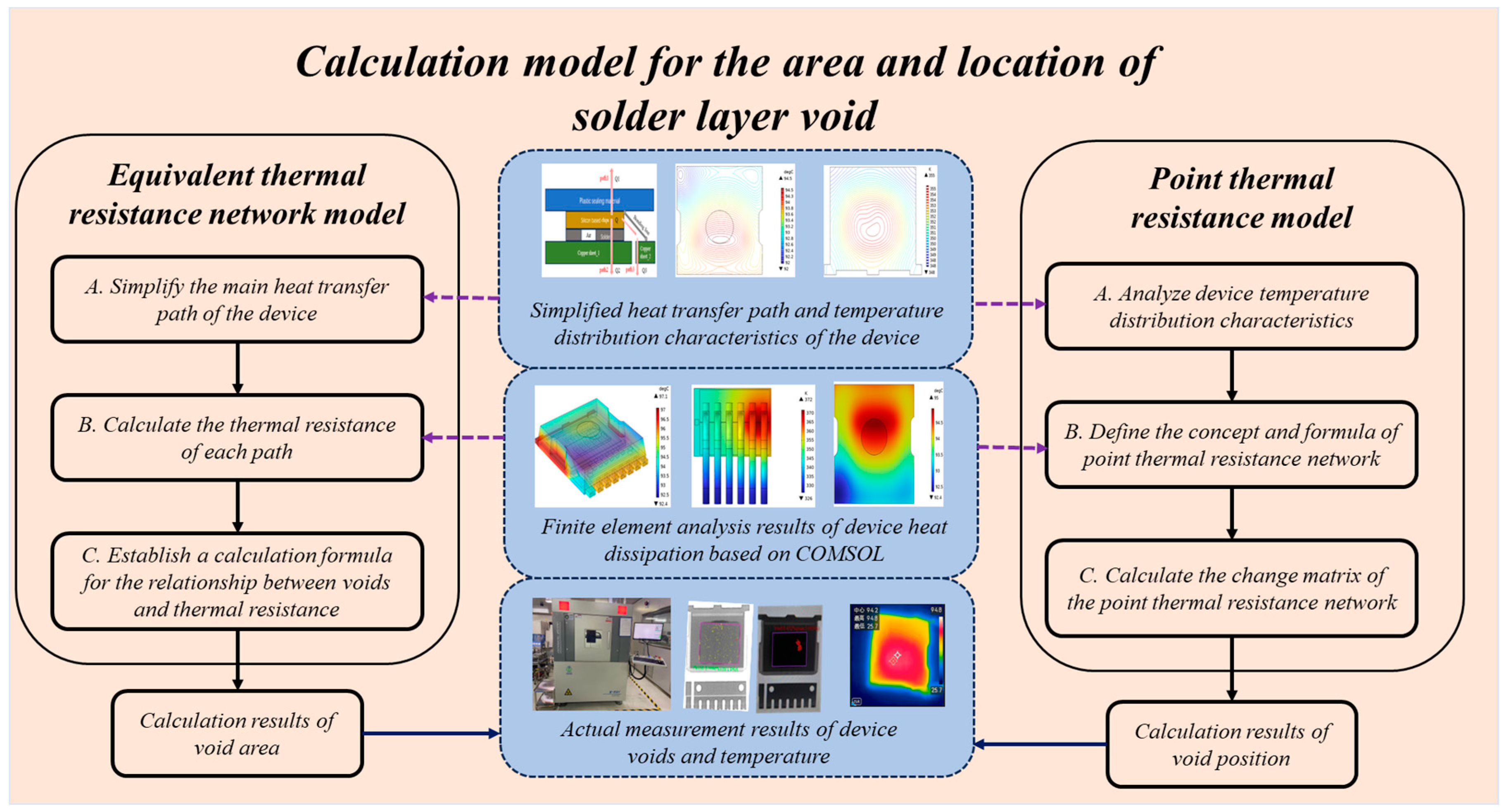
2. Void Area Calculation Model and Localization Model

Finite element analysis (FEA) is widely used in the thermal simulation of semiconductor power devices. In Section 2, the FEA method is used to establish a thermal resistance network model considering voids and the point thermal resistance location calculation model, based on a power MOSFET in a TOLL package shape. Figure 1 shows the overall structure diagram of the void area calculation and positioning models.

2.1. Modeling Process

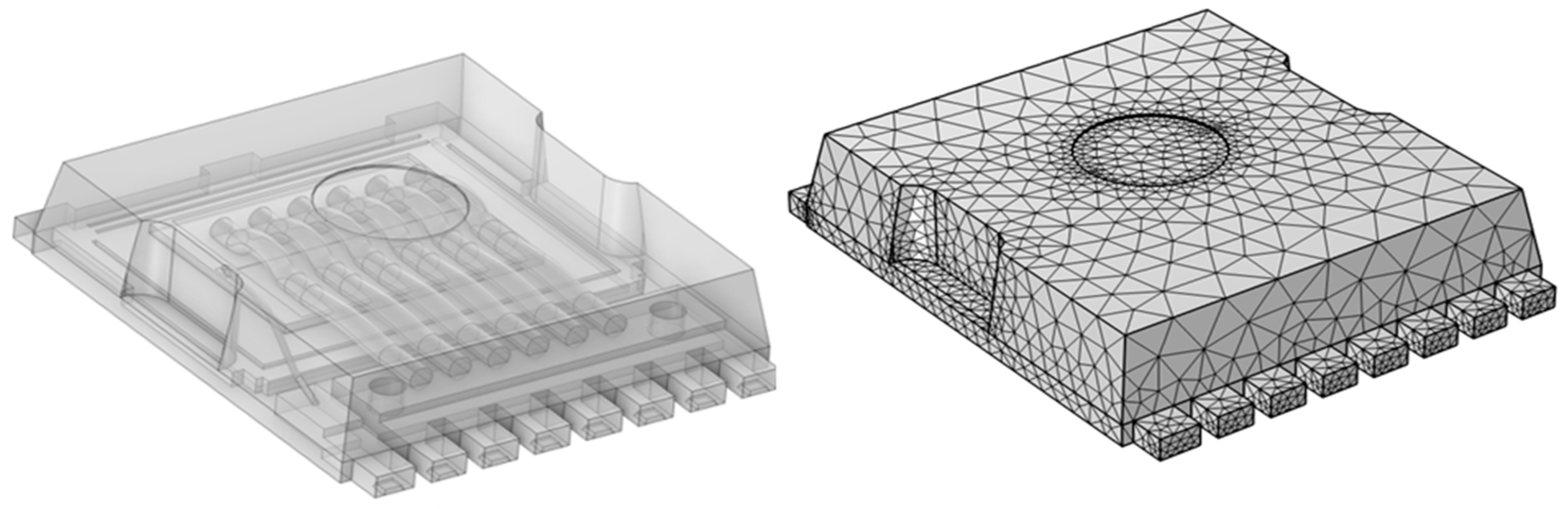
2.1.1. Finite Element Heat Transfer Thermal Calculation Model

The temperature distribution of a semiconductor device is a function of time and space, and based on the Fourier definition of heat transfer and the principle of conservation of energy, the computational expression of the heat transfer equation can be written as Equation (1):
x k x T x + y k y T y + z k z T z + Q = ρ c T t
where T is the temperature of the MOSFET chip, ρ is the density of the material, C is the specific heat capacity of the material, k x , k y , k z and are the thermal conductivity of the material along the x , y ,and z directions, respectively, and Q is the intensity of the internal heat source of the power device. In the steady-state heat transfer case, the temperature of each part of the device does not change with time, and for isotropic materials, Equation (1) can be rewritten as Equation (2):
0 = k 2 T x 2 + 2 T y 2 + 2 T z 2 + Q
k T n w = h T w T f
where n is the outer normal vector of the heat transfer surface, h is the convective heat transfer coefficient between the boundary and the air (this article takes h = 5 W/(m2·°C), and T w and T f are the temperature of the heat transfer boundary and the temperature of the surrounding air, respectively.
The TOLL package is a surface mount package that has a small volume, low parasitic parameters introduced by the package, and a high current-carrying capacity, so we take the MOSFET in the TOLL package as the object of study. Considering the complex geometry of the TOLL package, it is difficult to solve (2) and (3) by analytical methods. The finite element method can discretize the power device into several small units and solve the temperature of each unit to approach the real temperature distribution of the power device. The results of the device discretization are shown in Figure 2. It is worth noting that the main cause of power device heating is the chip’s internal resistance, basically having nothing to do with the package because the parasitic resistance of the package is at the milliohm level, which is much smaller than the internal resistance of the chip. At the same time, the bonding wire connection part of the contact thermal resistance, compared with the chip’s internal resistance, can be basically ignored. Therefore, in the simulation, the chip can be regarded as a heat source of equal intensity heat generation.

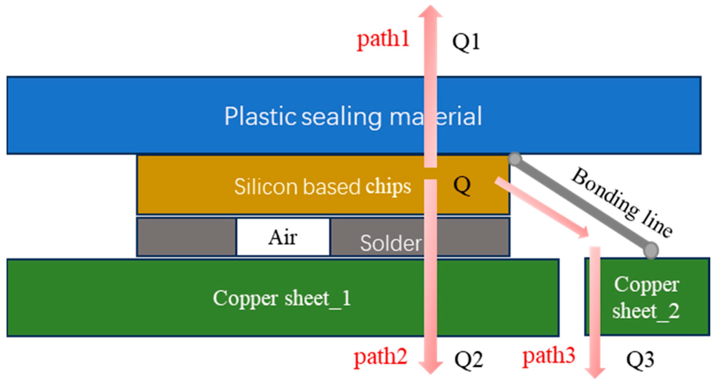
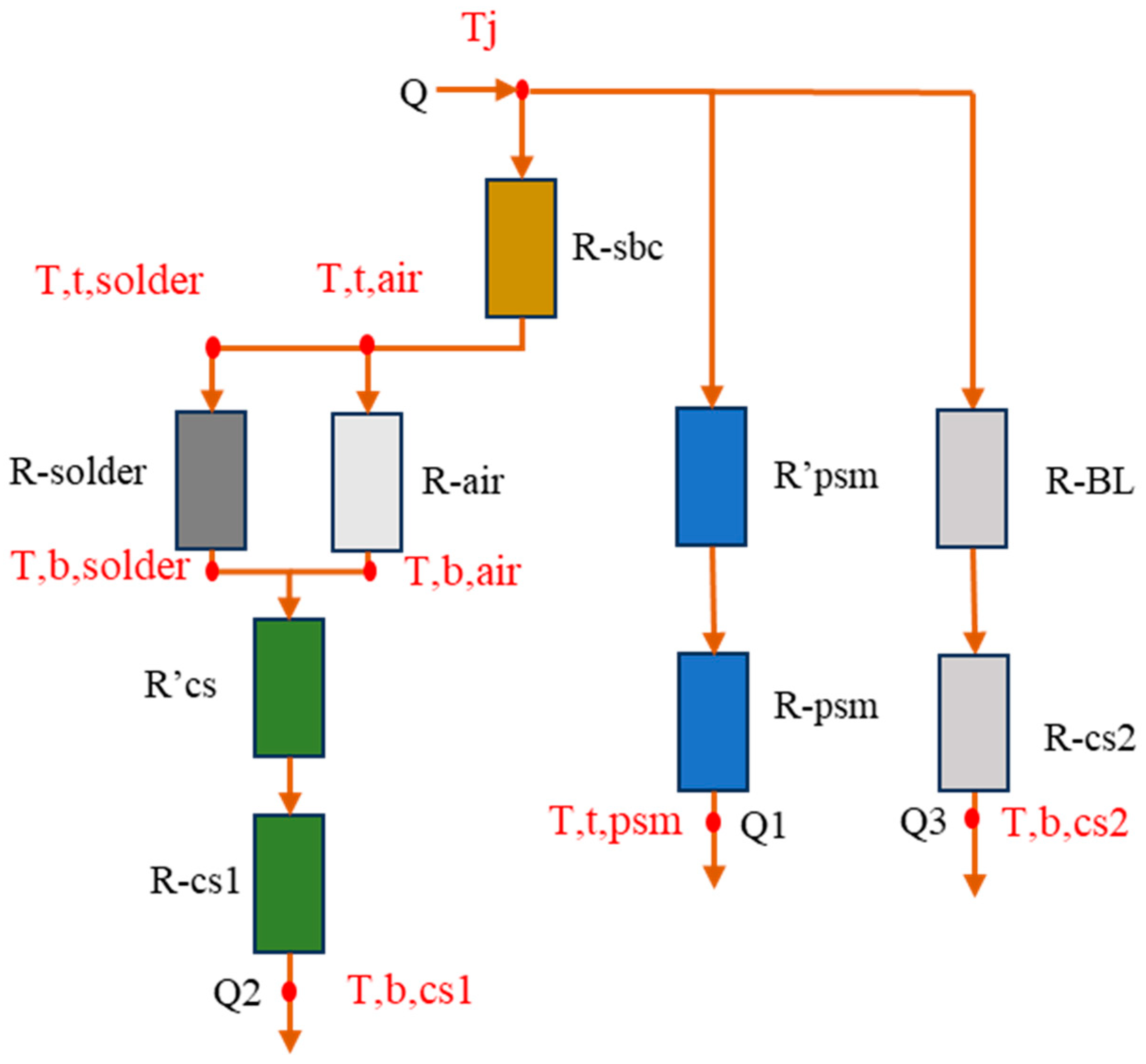
2.1.2. Equivalent Thermal Resistance Model Based on Major Heat Flow Paths

The solution results of the finite element method provide data support for the equivalent thermal resistance network model; based on the results of the finite element analysis, this paper simplifies the heat dissipation path of the device to three. As shown in Figure 3, the chip is the heat source of the power device. In the first heat dissipation path, the heat is transmitted to the air from the shell plastic sealing material; in the second path, the heat flows through the solder layer voids and the bottom of the copper diffusion to the air; and in the third heat dissipation path, the heat is conducted to the air through the bonding wire and the bottom of the copper.
Based on the three main heat transfer paths, the equivalent thermal resistance network of the device is shown in Figure 4. The thermal resistance of each path can be calculated from the ratio of the temperature difference to the heat flux intensity, and the expression for the path thermal resistance can be written as Equations (4)–(6):
R i path = T j T i Q i
Q = i = 1 3 Q i
Q i = S i h ( T i T f )
where R i path is the total thermal resistance of the i-th path, Q i is the intensity of the heat transfer in the i-th path, T i is the average temperature of the outer surface of the ith path, corresponding to T t , p s m , T b , c s 1 , and T b , c s 2 in Figure 4, respectively, and S i is the convective area of the i-th path for heat exchange with the air. The steady-state heat dissipation intensity of each path can also be derived based on the thermal resistance parallel shunt.
However, the overall thermal resistance calculation is not able to reflect the effect of the solder layer voids on the thermal resistance and temperature distribution of the device. Therefore, during the thermal resistance calculation for path 2, the thermal resistance of the voids is considered to be in parallel with the thermal resistance of the solder layer, and the main path thermal resistance network of the device can be calculated in a way that can be expressed by Equations (7) and (8):
R 0 1 path = R p s m + R p s m R 0 2 path = R air R solder R air + R solder + R s b c + R c s 1 + R c s 1 R 0 3 path = R B L + R c s 2
T t , air d s air + T t , solder d s solder ( T b , air d s air + T b , solder d s solder ) ( S air + S solder ) Q 2 = R air R solder R air + R solder
where R p s m is the diffusion thermal resistance between the chip and the plastic sealing material, R c s 1 is the diffusion thermal resistance between the solder layer and the copper sheet at the bottom, and R B L is the thermal resistance of the bonding line between the chip and the copper sheet; this part of the thermal resistance cannot be directly calculated by the material properties because of its irregular geometry, and it needs to be solved by associating the Equations (4)–(9). The thermal resistance of the plastic sealing material is R p s m , the thermal resistance of the air in the solder layer is R air , the thermal resistance of the solder layer is R solder , and the thermal resistance of the two copper sheets is R c s 1 and R c s 2 , respectively. These thermal resistances with regular shapes can be calculated by Equation (9):
R = L λ A
where L is the thickness of the material along the direction of the heat transfer path, L1 is the heat transfer coefficient of the material, and L2 is the surface area part of the material. The void ratio can be calculated from the ratio of void area to total area, and the calculation equations can be written as Equations (10) and (11):
S air + S solder = S
η = S air / S
where S air is the void area, S solder is the remaining solder layer area, and η is the void rate. Jointly with Equations (7)–(11), the incremental thermal resistance of the three paths after containing voids can be written as Equation (12). The thermal intensity of the device path 1 as a function of void area and void location can be written as Equation (13):
R 1 path = k 1 S air / S + R 0 2 path + k d 1 d R 2 path = L solder λ solder S L solder λ air η S + λ solder ( 1 η ) S + k 2 S air / S + R 0 2 path + k d 2 d R 3 path = k 3 S air / S + R 0 2 path + k d 3 d R air i path = 1 h S i + R i path
Q 1 = f ( η , d ) = Q 1 + R air 1 path   R air 2   path   + R air 3   path   / ( R air 2 path   R air 3 path   )
where L solder and λ solder are the thickness of the solder and its thermal conductivity, and λ air is the thermal conductivity of the air. The size and location of the void produces diffusion thermal resistance, which is positively correlated with the area of the void, η S , and the distance of the void from the center of the chip, d . In order to quantify the effect of the void on the thermal resistance, therefore, this paper defines k i as the void area diffusion coefficient, which is used to calculate the effect of the void area on the diffusion thermal resistance in the heat dissipation path, and k d i as the distance diffusion coefficient, which is used to calculate the effect of the center position on the diffusion thermal resistance in the heat dissipation path.

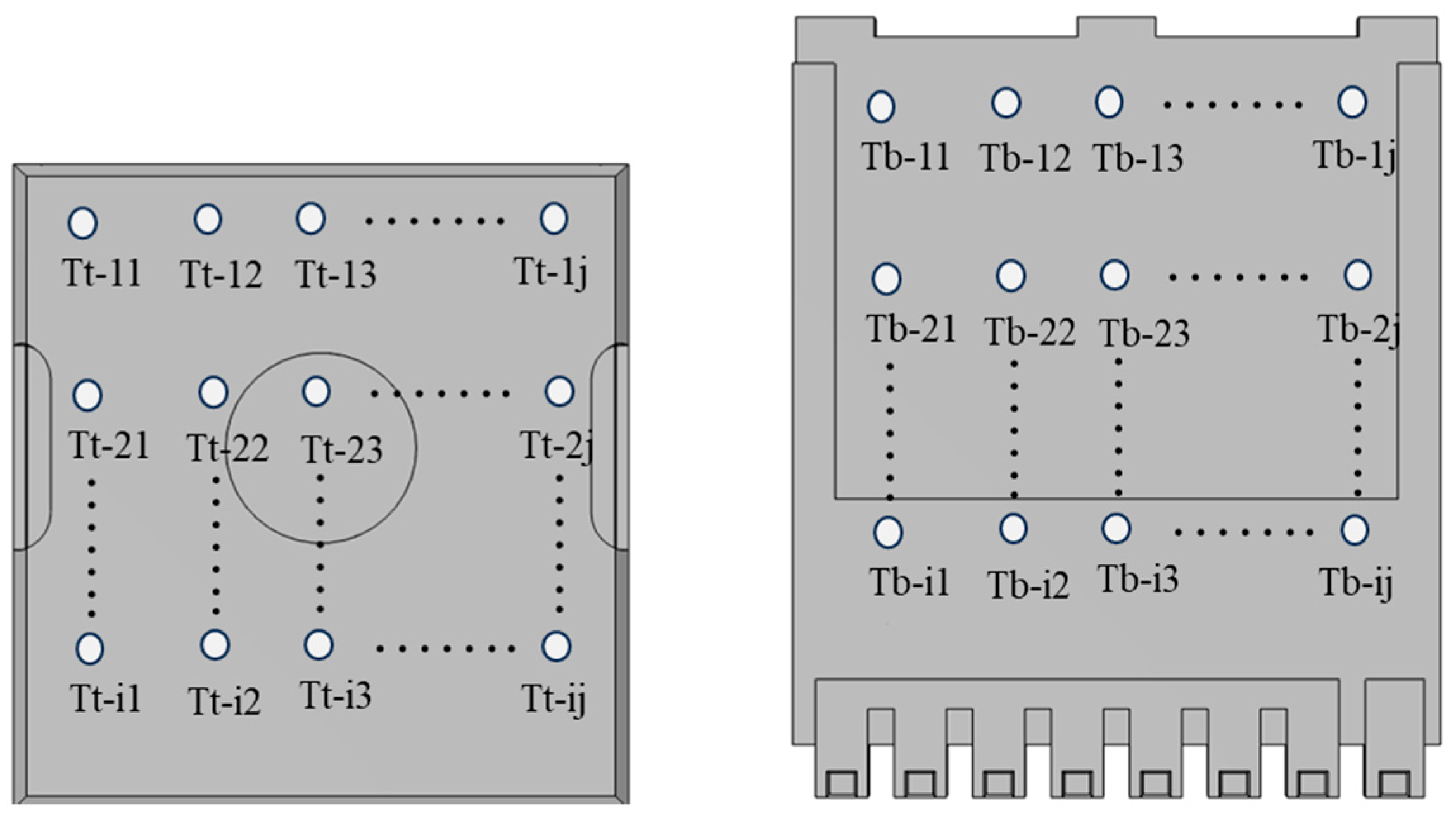
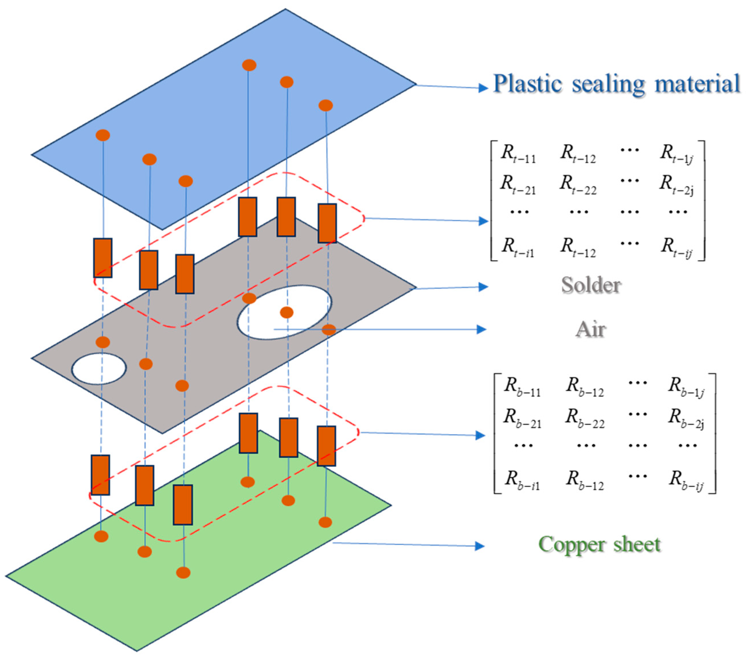
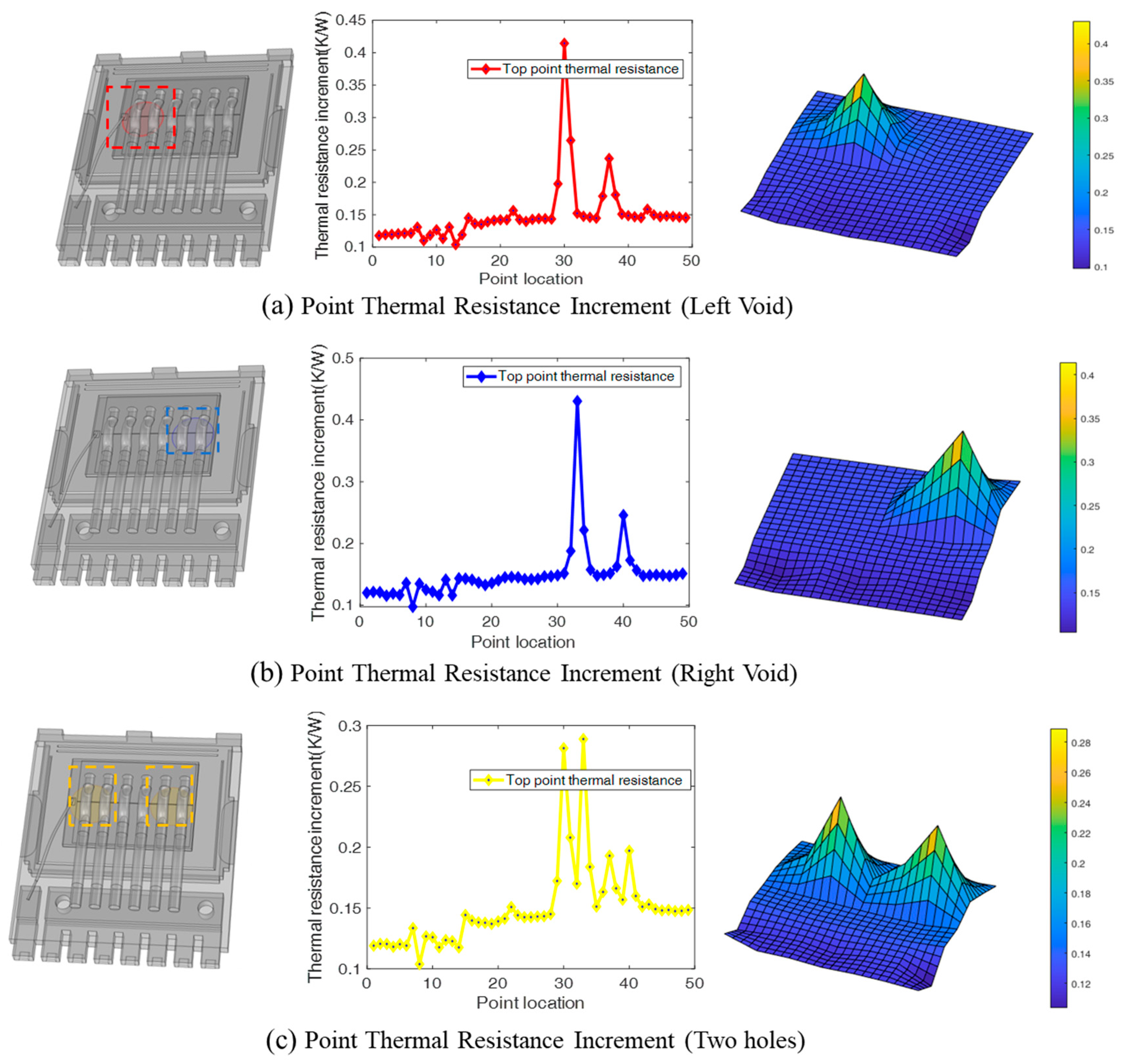
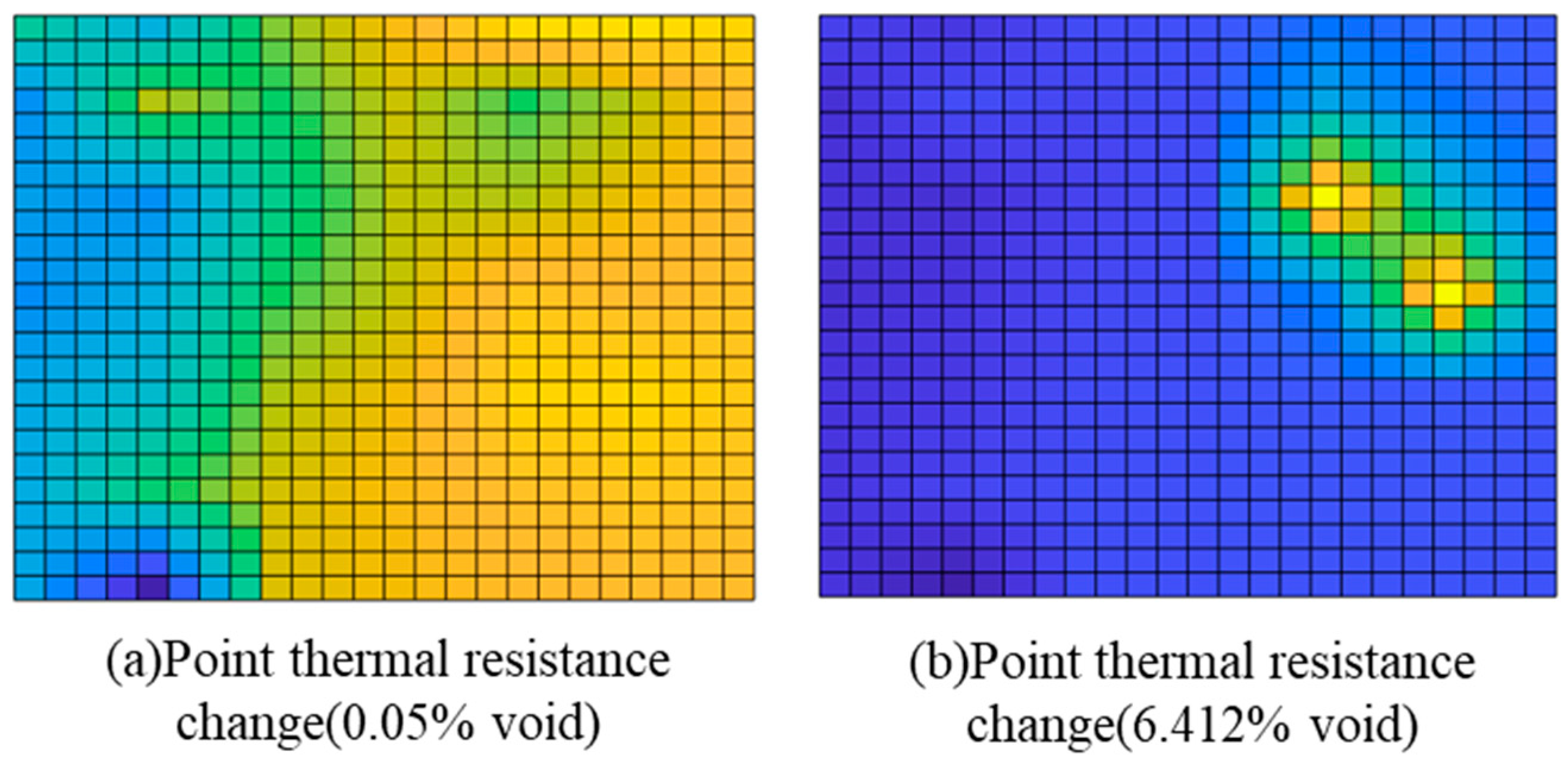
2.1.3. Calculation Model of Void Location Based on Point Thermal Resistance Network

Based on the calculated equivalent thermal resistance network model, this paper proposes a point thermal resistance model for calculating the location of solder voids. Specifically, the temperatures of i × j points on the top surface of the device are uniformly taken to form a temperature matrix, denoted as T t i j , and the temperatures of i × j points on the bottom surface of the device are uniformly taken to form a temperature matrix, denoted as T b i j . As shown in Figure 5, the points on the top surface and those on the bottom surface correspond to each other one by one. The structure of the point thermal resistance network model is given in Figure 6, and the thermal resistance of the taken points can be calculated by Equations (14) and (15):
T j I × J T t 11 T t 12 T t 1 j T t 21 T t 22 T t 2 j T t i 1 T t 12 T b i j = h ( T S 1 T f ) d s 1 × R t 11 R t 12 R t 1 j R t 21 R t 22 R t 2 j R t i 1 R t 12 R t i j
T j I × J T b 11 T b 12 T b 1 j T b 21 T b 22 T b 2 j T b i 1 T b 12 T b i j = h ( T S 2 T f ) d s 2 × R b 11 R b 12 R b 1 j R b 21 R b 22 R b 2 j R b i 1 R b 12 R b i j
In the formula, R t i × j and R b i × j are the point thermal resistance matrices at the top and bottom of the device, respectively, representing the thermal resistance from a point on the surface to the chip. They can be calculated by the temperature difference between the chip and the surface of the device, and T j I × J is the temperature distribution matrix of the chip, which can be directly taken as the average value of the chip temperature to facilitate the calculation.
When there are voids in the solder layer, the temperature distribution of the chip when it reaches steady state will change. For heat transfer path 1, the diffusive thermal resistance increases, the temperature distribution on the surface of the chip changes, and the dot thermal resistance matrix changes. For heat transfer paths 2 and 3, the voids lead to an increase in the thermal resistance of the solder layer along with the diffusion thermal resistance, and the temperature distribution at the bottom of the device changes. Therefore, in this paper, the variation of the point thermal resistance matrix is proposed to calculate the location of the solder layer voids, and the point thermal resistance variation matrix can be written as Equations (16) and (17):
Δ R t i × j = R t i × j R 0 t i × j
Δ R b i × j = R b i × j R 0 b i × j
where Δ R t i × j and Δ R b i × j are the changes in point thermal resistance at the top and bottom of the device, respectively. R 0 t i × j and R 0 b i × j are the point thermal resistance matrices at the top and bottom of the device, respectively, when there are no voids in the device.

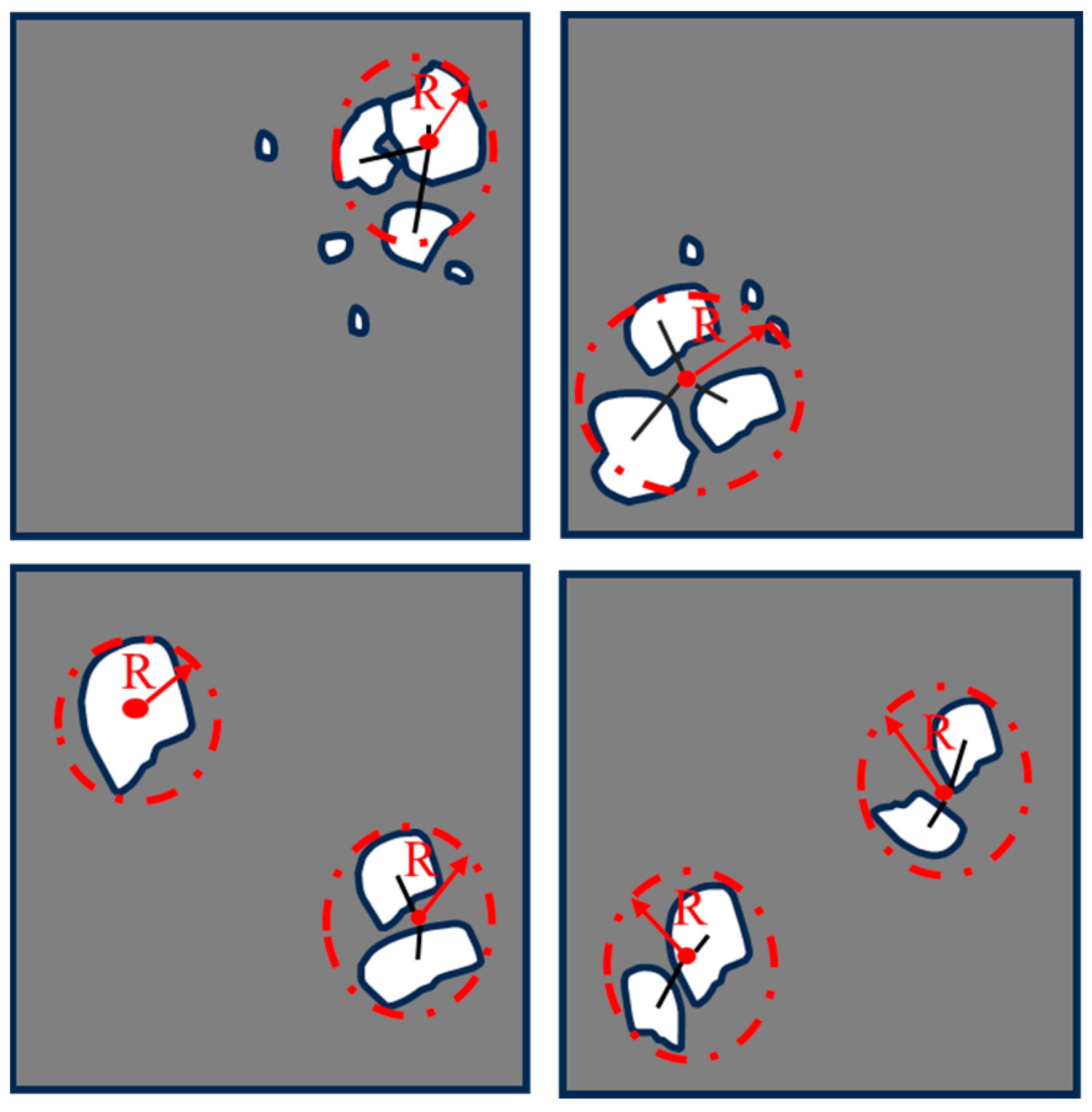
2.1.4. Equivalent Calculation of Area and Location of Solder Layer Voids

In fact, the initial distribution of voids in the solder layer does not have an obvious pattern, but as the device ages, the void rate will increase, and at the same time, the dispersed small voids will gradually merge into larger ones. In order to facilitate the simulation calculation, we need to equate the discrete voids; the equating process is shown in Figure 7, and the equating calculation is shown in Equations (18)–(21):
i = 1 n S h i = S H
R h = S H π
[ X center Y center ] = S h 1 S H S h i S H x 1 x i y 1 y i
( x i x j ) 2 + ( y i y j ) 2 W 2
where S h i is the area of the i-th voids, S H is the total area of the voids, R h is the equivalent radius of the area of the voids, ( X center , Y center ) is the equivalent geometric center of the voids, and W is the width of the solder layer. Equation (21) shows that there are multiple equivalent centers of the voids and equivalent areas of the voids when they are distributed far away from each other.

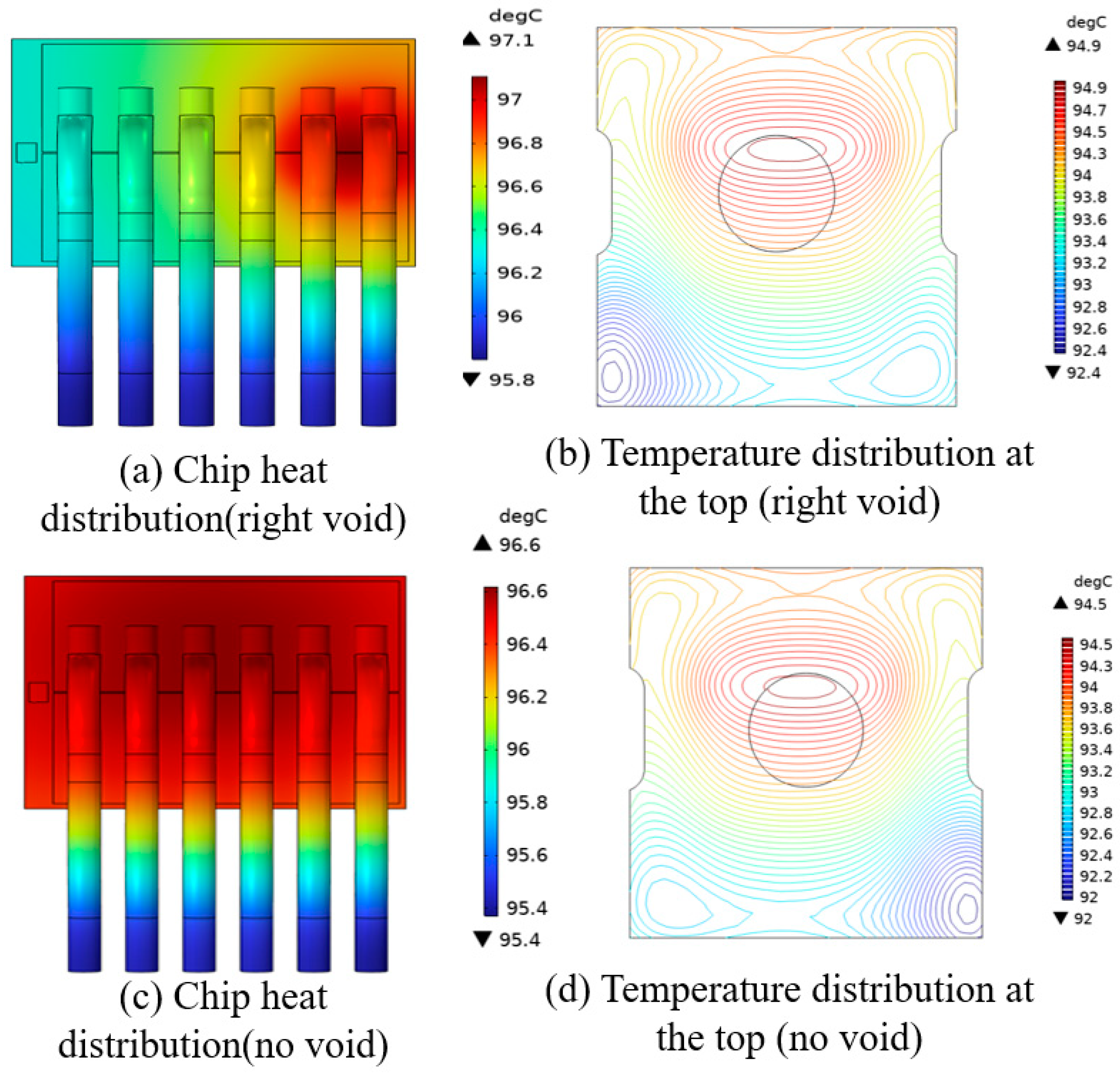
2.2. Simulation Results and Discussion

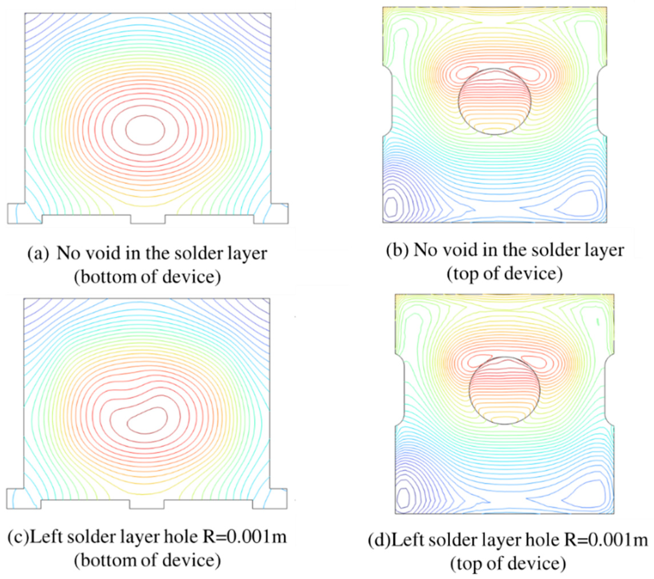
Effect of Voids on Device Temperature Distribution

In order to verify that the temperature distribution of the device is affected by voids, the distribution of isotherms at the top and bottom of the device is given in Figure 8. When there are no voids in the solder layer, the isotherms at the bottom have an elliptical distribution, and when there are voids in the solder layer, the isotherms appear to be curved at the locations where the voids are present. Similarly, this is the case for the top. Thus, the point thermal resistance network model that contains the temperature distribution characteristics of the device has the ability to reflect the solder layer voids. The materials of the devices are given in Table 1.
In order to investigate the heat transfer mechanism of the device when containing voids, it is necessary to discuss the temperature distribution of the solder layer. The temperature distribution of the solder layer with and without voids is given in Figure 9. For the case of dissipated power p = 0.37 W, the temperature distribution of the solder layer with and without voids is shown in Figure 8a. From Figure 8a, it can be seen that heat accumulation occurs at the location of the solder layer voids, and the temperature is significantly higher than that at other locations, while the overall temperature of the solder layer without voids is lower than that of the case with voids. When there is a void, the center of the isotherm at the top of the device is shifted to the center of the void, and at the same time, the temperature of the device surface is higher than the temperature of the device surface when there are no voids.

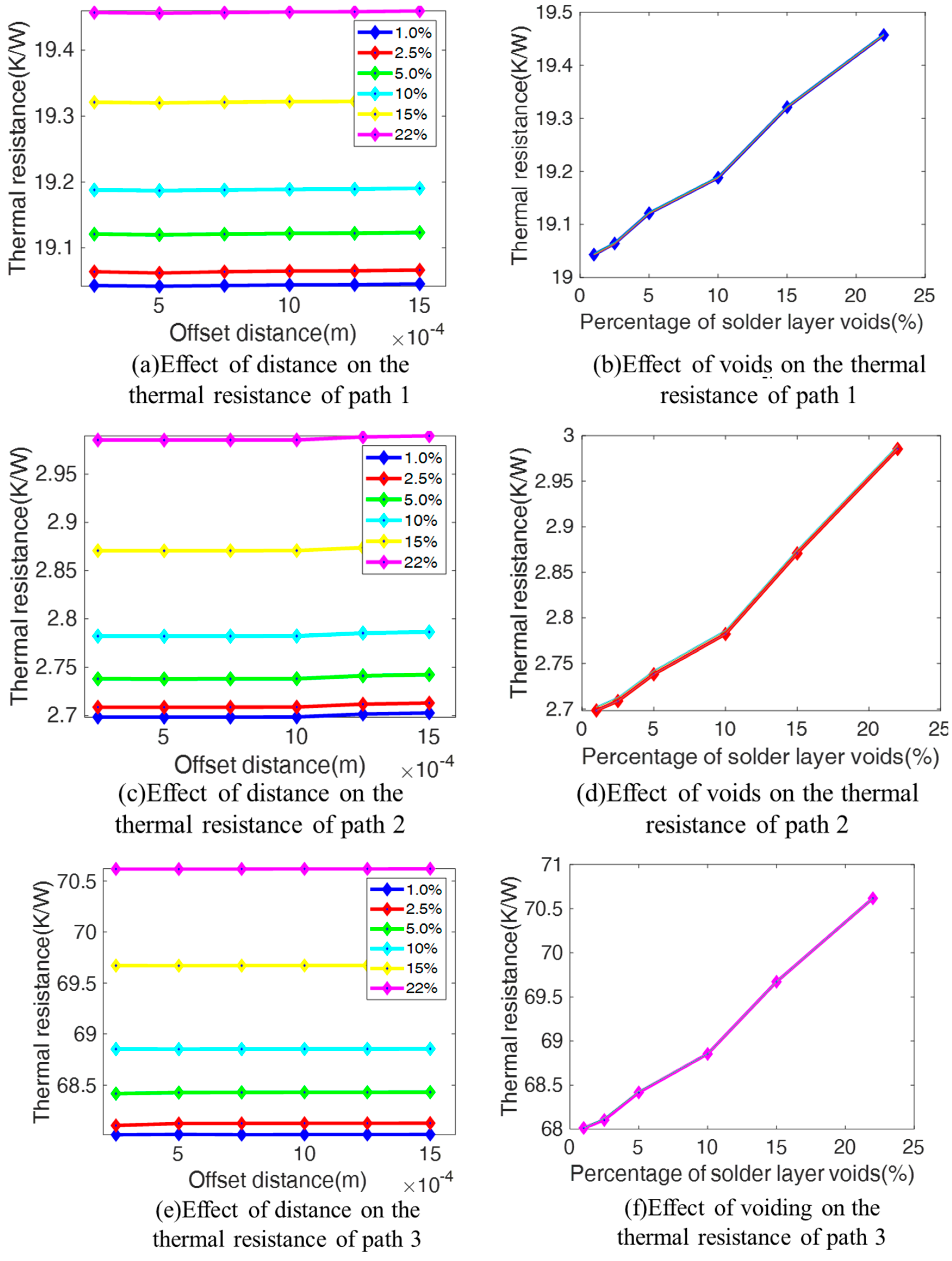
2.3. Effect of Voids on Thermal Resistance of Heat Transfer Paths

Voids not only affect the temperature distribution of the device, but also affect the thermal resistance of the heat sink path. Figure 10 gives the effects of the void rate and the location of the void on the thermal resistance of the heat sink path. Figure 10a,c,e compare the variation in thermal resistance with the different offset positions of the voids. It can be seen that the position of the existence of the voids has basically no effect on the thermal resistance of the three paths, and the size of the voids is the most important factor affecting the thermal resistance of the paths. From Figure 10b,d,f, it can be seen that the heat dissipation paths all increase with the increase in solder layer voids. The thermal resistance of heat dissipation path 2 has the largest growth rate under the influence of voids, and the thermal resistance of path 1 has the smallest growth rate; therefore, the voids lead to a decrease in heat dissipation at the bottom of the device and an increase in heat dissipation at the top.
According to the results discussed above, the influence of the void location on thermal resistance is small and basically negligible compared to the void area. Therefore, k d i = 0 in Equation (13); in addition, the area diffusion coefficient can be obtained by fitting, and the results are k 1 = 0.02 , k 2 = 0.015 , and k 1 = 0.12 . Taking path 2 as an example, a comparison of the thermal resistance values calculated by Equation (13) with those calculated by simulation is shown in Figure 11. The maximum error in the calculation of thermal resistance is 4% for a void rate of 0–25%, and the error decreases as the void rate increases.
In Figure 12a–c, the point thermal resistance variation matrices are given when the solder layer contains one void on the left side, one void on the right side, and voids on both the left and right sides, respectively. The line graph in Figure 11 has 7 × 7 = 49 points, which are uniformly distributed on the surface of the device. This paper captures the distribution of internal voids in the device by calculating the changes in thermal resistance values at these locations. From Figure 12, it can be clearly seen that the location of the hole is the location of the largest change in the point thermal resistance, and the point thermal resistance calculation results can be a good reflection of the shape and location of the void in the solder layer.
As shown in Figure 13, the point thermal resistance change matrix can visualize the shape and location of the solder layer voids. Therefore, under the condition of sufficient computational resources, the larger the number of temperature-taking points, the finer the division of the unit area; the void area of the solder layer can also be estimated by calculating the area of the yellow part.

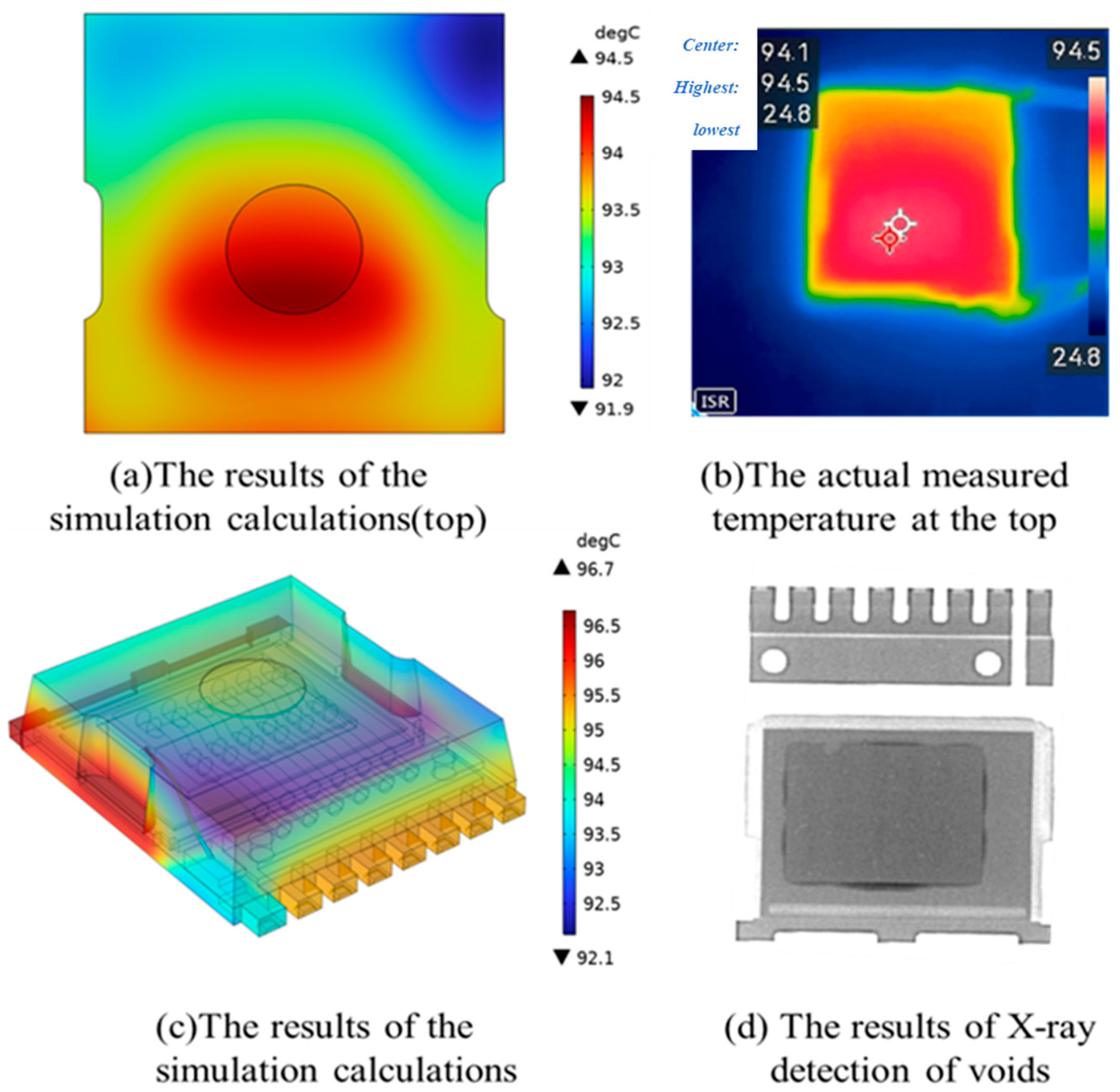
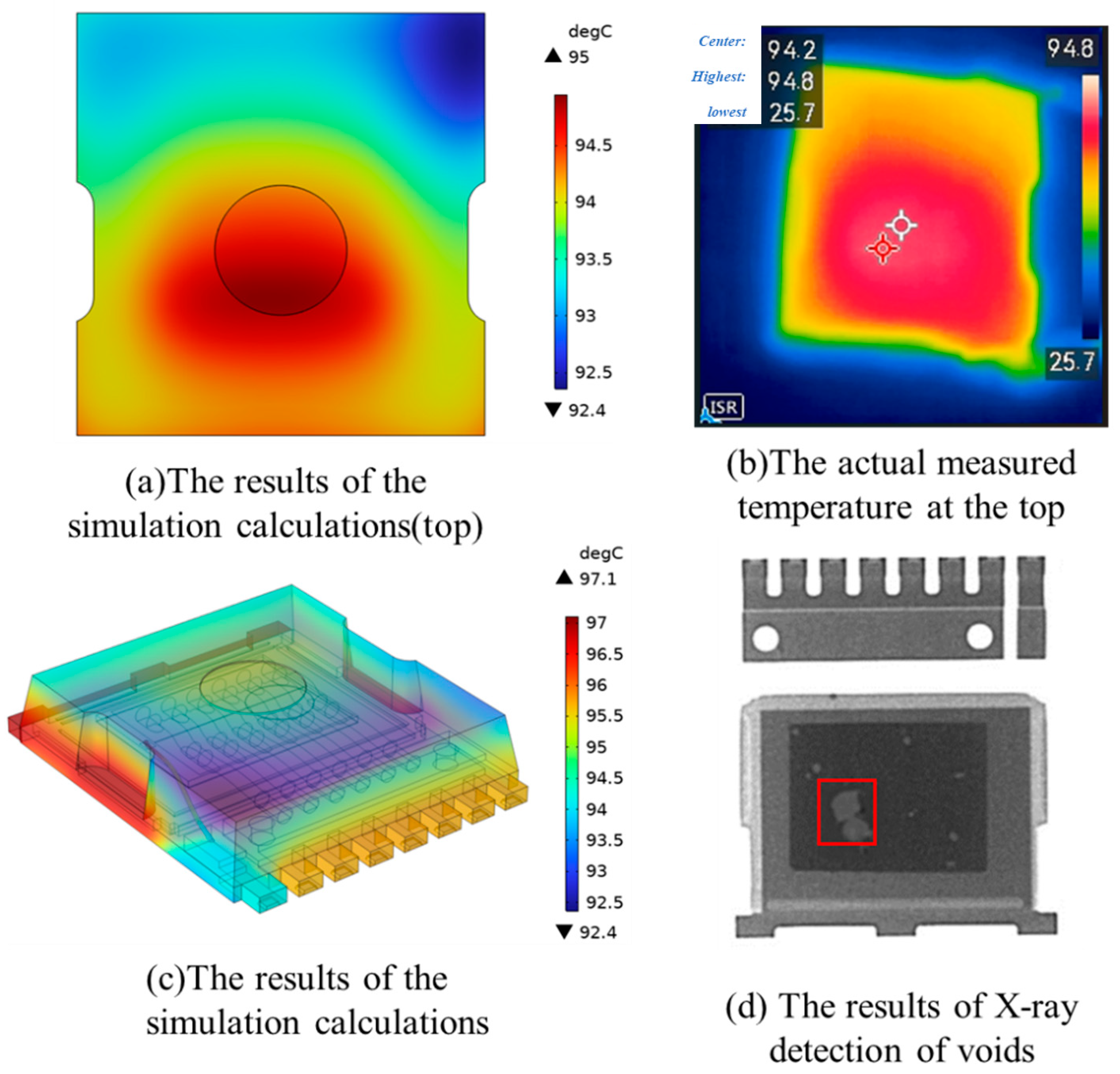
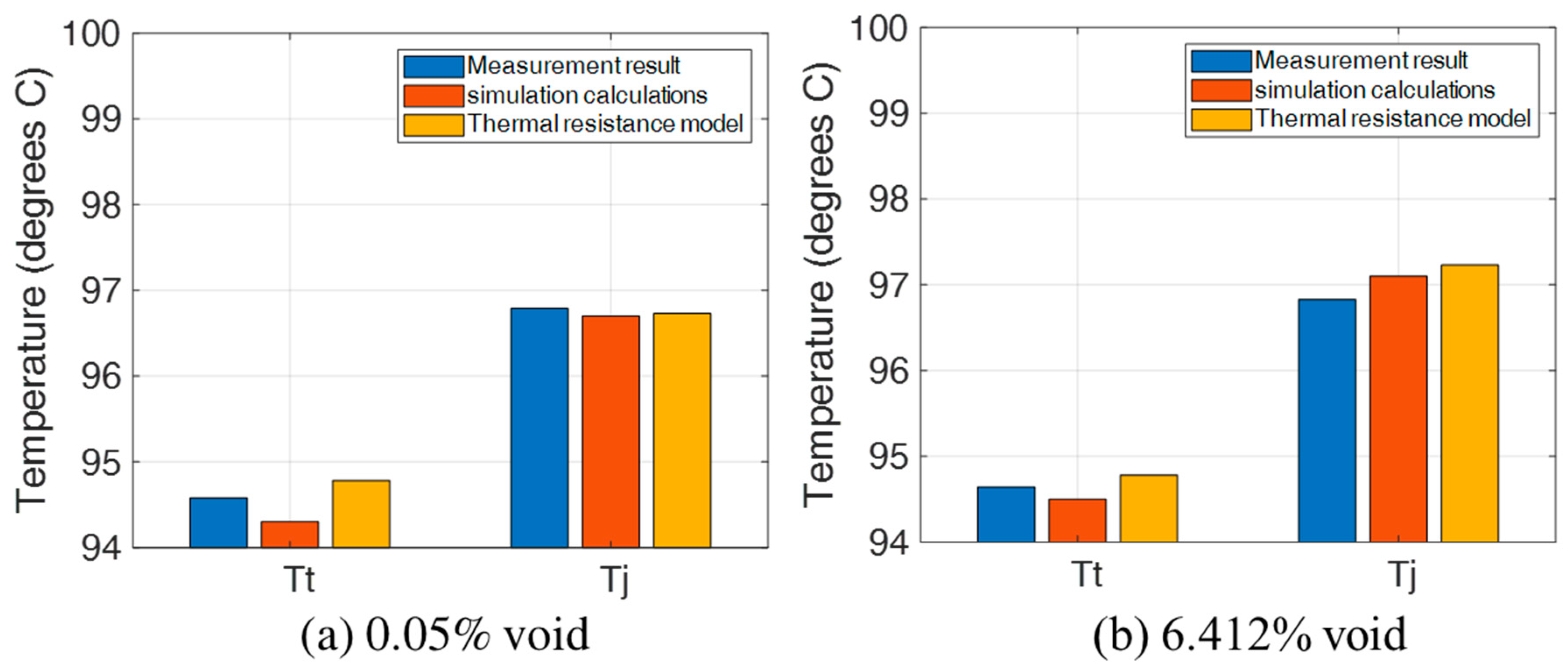
3. Comparison between Measurement Results and Calculation Results

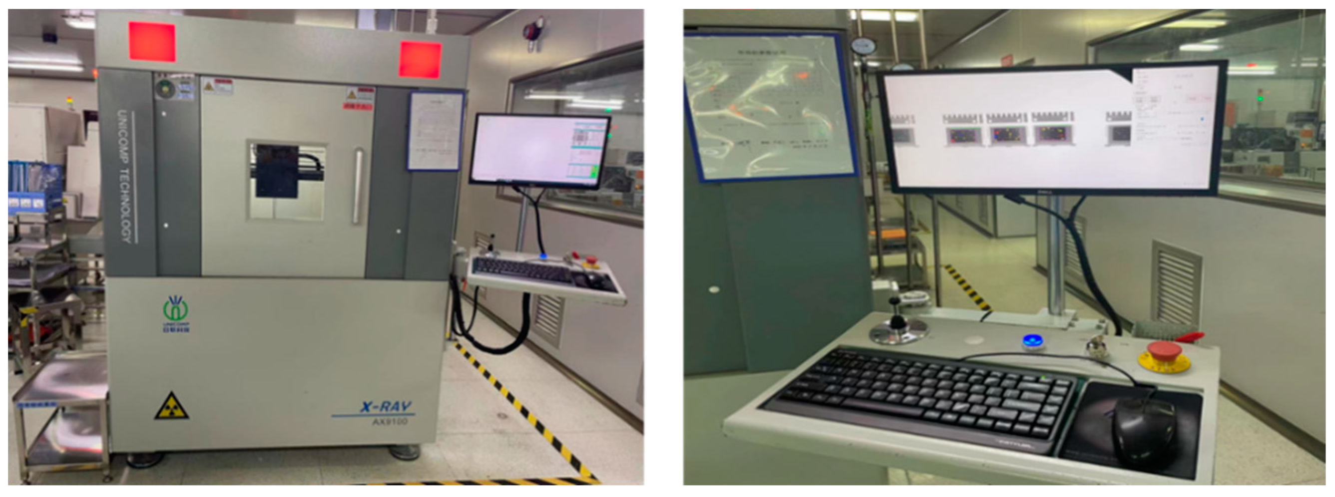
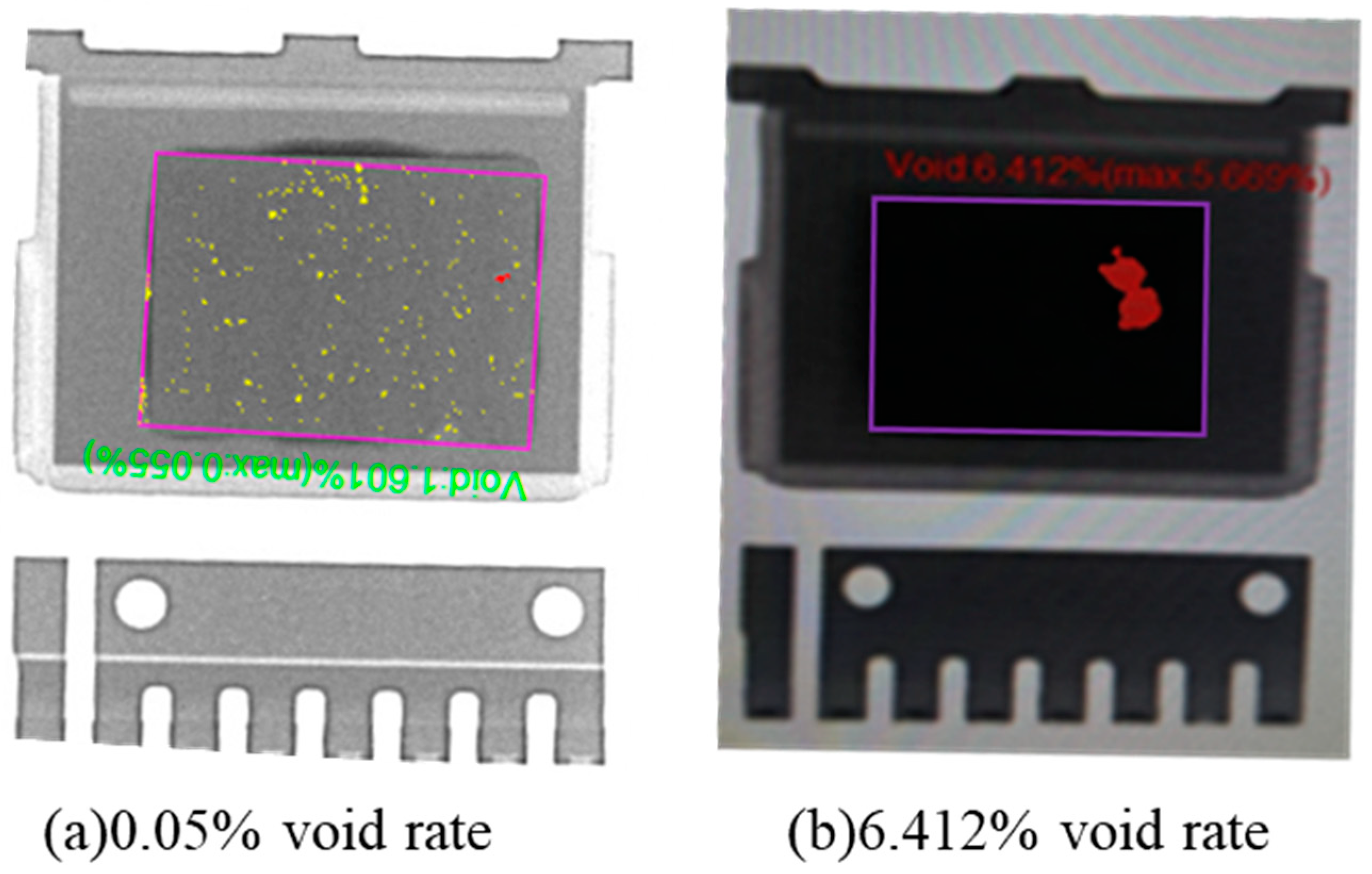
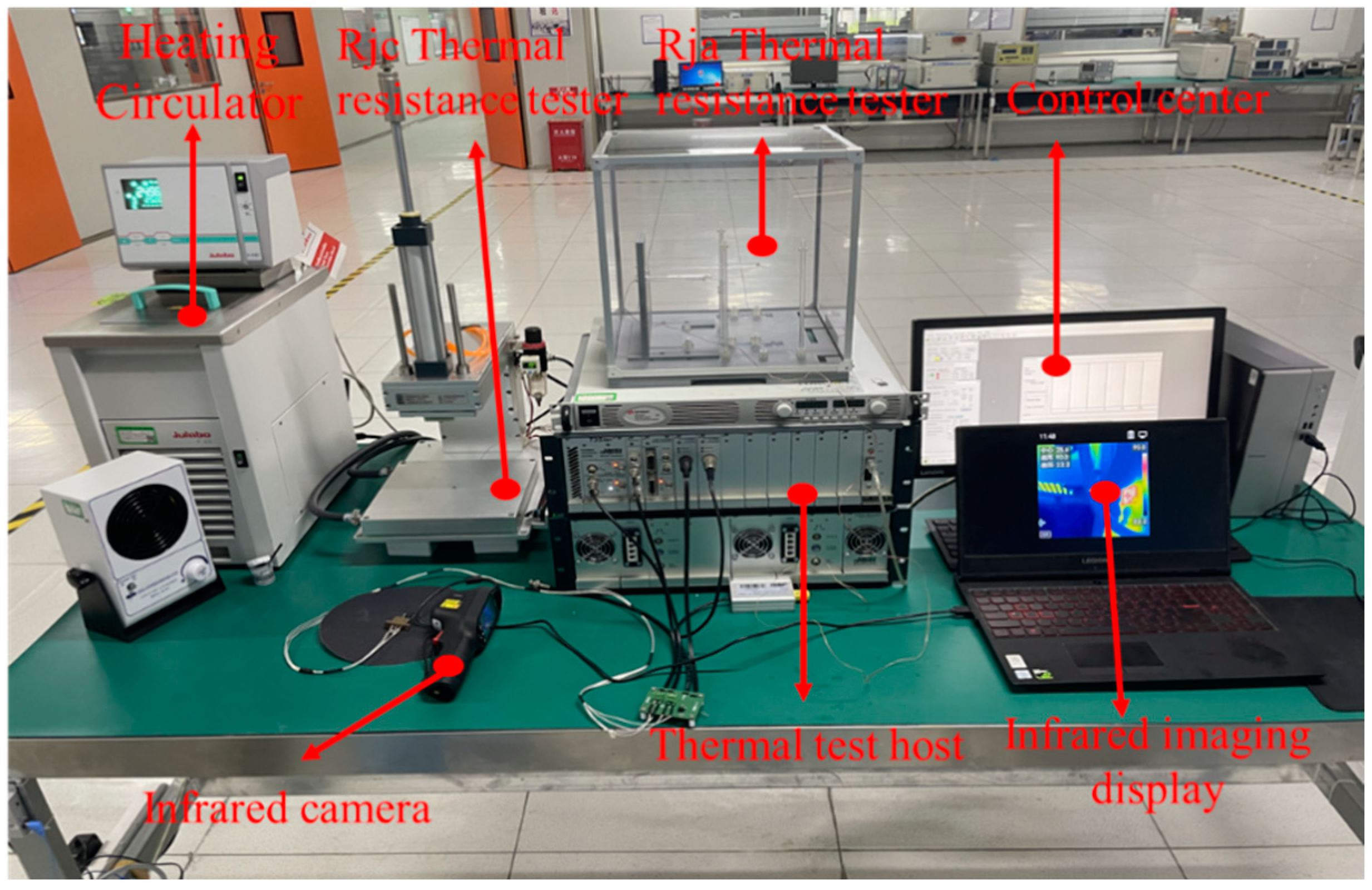
Experimental Platform for X-ray Void Rate Detection

In order to compare the difference between the experimental measurements and the theoretical calculations, two TOLL-packaged devices were screened as measurement objects in this paper. Through the X-ray void detector in Figure 14, it was determined that one of them had a void rate of 0.05% and the other one had a void rate of 6.412%, and the results are shown in Figure 15.
Based on the infrared thermography and thermal resistance test platform in Figure 16, the temperature distribution of the device was measured. Figure 17 shows the principle of device heating and junction temperature detection; firstly, the temperature is increased by the circuit in Figure 17a; when the temperature basically reaches the steady state, the DC source outputs a small current, and the voltage drop of the body diode is measured at this time; and finally, the junction temperature (Tj) can be determined by the curve in Figure 17b.
Figure 18 and Figure 19 show the temperature distribution of the device when the void ratios of the solder layer are 0.05% and 6.412%, respectively, and it can be seen that the simulation results are basically consistent with the experimental measurements. When the void rate increases, the temperature of the surface of the device increases, and the highest value of the temperature is closer to the position where the void exists. When the void rate is 0.05%, the difference between the surface temperature and the Tj of the device is 2.3 °C, and when the void rate is 6.412%, the difference is 2.7 °C, therefore, the temperature difference between the surface of the device and the device chip increases due to the presence of voids, which also indicates that the voids lead to an increase in the thermal resistance of the heat dissipation path. The heat source intensity value Q in the simulation is equal to the heating power. The heating power is calculated by multiplying the current flowing through the device by the voltage drop of the device, which can also be obtained using the T3ster thermal resistance experimental platform.
According to Equations (13) and (14), or according to the simulations, the thermal resistance value of the path can be calculated from the void rate, and the void rate can also be calculated from the thermal resistance value. Figure 20a gives the calculation results of solving the thermal resistance value with the known void ratio, and Figure 20b gives the calculation results of solving the void ratio of the solder layer with the known thermal resistance.
It can be seen from Figure 20 that there are errors between the simulation results and the measurement calculation results, which mainly consist of two parts. Specifically, the first part of the error may come from the measurement of the temperature: the measurement of temperature cannot reflect the actual temperature distribution of the device, which may lead to the deviation of the cavity positioning results. Another part of the error comes from the simplification process of the model: in order to improve the calculation speed of the model, some details may be ignored during the simulation. For example, in the design, the chip and the solder layer have the same size (excepting thickness), but due to the limitation of the core-loading process, the solder layer is actually larger than the chip size, which makes the simulation result of the thermal resistance smaller than the calculation result.
Figure 21 shows the results of the actual measurement, the finite element simulation calculation, and the thermal resistance network calculation, respectively, for the top temperature, Tt, of the device and the chip temperature, Tj. The difference between the top temperatures and the junction temperatures derived from these three ways is very small; in terms of calculation speed and practical ease of operation, the proposed main heat flow path network model has a greater advantage, but it is also necessary to model and simulate the device in advance to find the thermal resistance value of each path.
The point thermal resistance variation of the device with a void rate of 0.05% is shown in Figure 22a, and it is impossible to judge the location of the void from the point thermal resistance variation value. In Figure 21b, the point thermal resistance variation value of the device with a void rate of 6.412% is shown, and the yellow part in the upper right corner is the maximum value; this long strip-like region is judged to be a void. Comparing with the X-ray void detection results in Figure 14, the location of the voids matches the calculation results of the point thermal resistance model.

4. Results and Discussion

In this paper, the area and location of solder layer voids are calculated by combining finite element calculations and experiments. The temperature distribution characteristics of the device in the TOLL package are calculated through finite element simulation, and the equivalent thermal resistance network model considering the effect of voids is proposed for calculating the void area. Based on the temperature distribution characteristics and the equivalent thermal resistance calculation results, a point thermal resistance model is proposed to calculate the location of the voids. Finally, the validity of the proposed method is verified by comparing the data from the simulation calculations and the actual measurements. The conclusions drawn in this paper are as follows:
  • The thermal resistance of the device is basically unaffected by the location of the solder layer voids, while the area of the solder layer voids has a greater impact on the thermal resistance; the voids are in the range of 5–25%, and the area of the voids is positively and linearly correlated with the thermal resistance of the heat dissipation paths.
  • The voids in the solder layer lead to an increase in the thermal resistance of the main heat dissipation paths inside the device and to the accumulation of heat at the location of the voids.
  • The maximum value of the point thermal resistance change matrix is the center of the void, and the approximate extent of the void can be determined by the range in which the matrix change occurs.
There is some error between the calculated results and the measured results, which is caused by the measurement error of the device temperature. Therefore, the selection of more accurate temperature measurement instruments to improve the accuracy of the calculation is one of our future works. At the same time, it is convenient to evaluate the reliability of power devices by temperature measurement, so it is our future work to improve the model proposed in this paper and apply it in real circuits.

Author Contributions

Conceptualization, W.G. and X.C.; Methodology, W.G. and X.C.; Software, Z.T.; Validation, W.G. and Z.T.; Formal analysis, W.G.; Resources, X.L. and Z.M.; Data curation, W.G.; Writing—review & editing, X.C.; Visualization, X.L. and D.X.; Supervision, Z.M. and X.X.; Project administration, D.X.; Funding acquisition, X.L. All authors have read and agreed to the published version of the manuscript.

Funding

This work was supported by the Tianfu Yongxing Laboratory Science and Technology Innovation Project (2023CXXM15) and the Science and Technology Research Program of Chongqing Municipal Education Commission (No. KJZD-K202101103).

Data Availability Statement

The data presented in this paper are available upon request from the corresponding author.

Conflicts of Interest

Authors Xiangtao Xu and Daquan Xia were employed by the company Chongqing Pingwei Enterprise Co., Ltd. The remaining authors declare that the research was conducted in the absence of any commercial or financial relationships that could be construed as a potential conflict of interest.

References

  1. Alatise, O.; Deb, A.; Bashar, E.; Ortiz Gonzalez, J.; Jahdi, S.; Issa, W. A Review of Power Electronic Devices for Heavy Goods Vehicles Electrification: Performance and Reliability. Energies 2023, 16, 4380. [Google Scholar] [CrossRef]
  2. Aharon, I.; Kuperman, A. Topological overview of powertrains for battery-powered vehicles with range extenders. IEEE Trans. Power Electron. 2011, 3, 868–876. [Google Scholar] [CrossRef]
  3. Scheuermann, U. Reliability challenges of automotive power electronics. Microelectron. Reliab. 2009, 49, 1319–1325. [Google Scholar] [CrossRef]
  4. Quintero, P.O.; McCluskey, F.P. Temperature cycling reliability of high-temperature lead-free die-attach technologies. IEEE Trans. Device Mater. Reliab. 2011, 11, 531–539. [Google Scholar] [CrossRef]
  5. Li, Y.; Fu, G.; Wan, B.; Wu, Z.; Yan, X.; Zhang, W. A study on the effects of electrical and thermal stresses on void formation and migration lifetime of Sn3.0Ag0.5Cu solder joints. Solder. Surf. Mt. Technol. 2022, 3, 162–173. [Google Scholar] [CrossRef]
  6. Lu, Y.; Christou, A. Lifetime estimation of insulated gate bipolar transistor modules using two-step bayesian estimation. IEEE Trans. Device Mater. Reliab. 2017, 17, 414–421. [Google Scholar] [CrossRef]
  7. Cui, H.; Zhou, M.; Yang, C.; Li, J.; Wang, C. Influence mechanism of solder aging and thermal network model optimization of multi-chip IGBT modules. Microelectron. Reliab. 2022, 139, 114827. [Google Scholar] [CrossRef]
  8. Huang, Y.; Luo, Y.; Xiao, F.; Liu, B.; Tang, X. Temporal and spatial differences in thermal transfer behavior of IGBTs caused by the baseplate and die-attach solder cracking. IEEE J. Emerg. Sel. Top. Power Electron. 2020, 10, 7177–7187. [Google Scholar] [CrossRef]
  9. Jia, Y.; Huang, Y.; Xiao, F.; Deng, H.; Duan, Y.; Iannuzzo, F. Impact of solder degradation on Vce of IGBT module: Experiments and modeling. IEEE J. Emerg. Sel. Top. Power Electron. 2020, 10, 4536–4545. [Google Scholar] [CrossRef]
  10. Frede, B.; Marco, L.; Ma, K. Power electronics converters forwind turbine systems. IEEE Trans. Ind. Appl. 2012, 48, 708–719. [Google Scholar]
  11. Otiaba, K.C.; Bhatti, R.S.; Ekere, N.N.; Mallik, S.; Alam, M.O.; Amalu, E.H.; Ekpu, M. Numerical study on thermal impacts of different void patterns on performance of chip-scale packaged power device. Microelectron. Reliab. 2012, 12, 1409–1419. [Google Scholar] [CrossRef]
  12. Du, M.; Guo, Q.; Wang, H.; Ouyang, Z.; Wei, K. An improved cauer model of IGBT module: Inclusive void fraction in solder layer. IEEE Trans. Compon. Packag. Manuf. Technol. 2020, 10, 1401–1410. [Google Scholar] [CrossRef]
  13. Okereke, M.I.; Ling, Y. A computational investigation of the effect of three-dimensional void morphology on the thermal resistance of solder thermal interface materials. Appl. Therm. Eng. 2018, 142, 346–360. [Google Scholar] [CrossRef]
  14. Kenny, C.; Okereke, M.I.; Bhatti, R.S. Numerical assessment of the effect of void morphology on thermo-mechanical performance of solder thermal interface material. Appl. Therm. Eng. 2014, 64, 51–63. [Google Scholar]
  15. Li, Q.; Zhang, F.; Chen, Y.; Fu, T.; Zheng, Z. A junction temperature model based on heat flow distribution in an IGBT module with solder layer voids. Heliyon 2024, 10, 25–33. [Google Scholar] [CrossRef] [PubMed]
  16. Li, H.; Hu, Y.; Liu, S.; Li, Y.; Liao, X.; Liu, Z. An improved thermal network model of the IGBT module for wind power converters considering the effects of base-plate solder fatigue. IEEE Trans. Device Mater. Reliab. 2016, 16, 570–575. [Google Scholar] [CrossRef]
  17. Fan, Y.; Cui, H.; Lou, Z.; Teng, J.; Tang, Z.; Peng, J. Base solder voids identification of IGBT modules using case temperature. Microelectron. Reliab. 2020, 115, 113968. [Google Scholar] [CrossRef]
  18. Kim, K.S.; Huh, S.H.; Suganuma, K. Effects of cooling speed on microstructure and tensile properties of Sn–Ag–Cu alloys. Mater. Sci. Eng. 2002, 333, 106–114. [Google Scholar] [CrossRef]
  19. Amalu, E.H.; Ekere, N.N. Modelling evaluation of GarofaloArrhenius creep relation for lead-free solder joints in surface mount electronic component assemblies. J. Manuf. Syst 2016, 39, 9–23. [Google Scholar] [CrossRef]
  20. Wang, C.; He, Y.; Wang, C.; Li, L.; Wu, X. Multi-Chip IGBT Module Failure Monitoring Based on Module Transconductance with Temperature Calibration. Electronics 2020, 9, 1599. [Google Scholar] [CrossRef]
  21. Samavatian, V.; Iman-Eini, H.; Avenas, Y.; Samavatian, M. Effects of creep failure mechanisms on thermomechanical reliability of solder joints in power semiconductors. IEEE Trans. Power Electron. 2020, 35, 8956–8964. [Google Scholar] [CrossRef]
  22. Hu, B.; Konaklieva, S.; Kourra, N.; Williams, M.A.; Ran, L.; Lai, W. Long-term reliability evaluation of power modules with low amplitude thermomechanical stresses and initial defects. IEEE J. Emerg. Sel. Top. Power Electron. 2021, 9, 602–615. [Google Scholar] [CrossRef]
  23. Liu, Y.; Jia, L.; Wang, L.; Wang, J.; Zhang, J.; Zhang, Z. An Accurate and Intelligent Approach to Predicting the Power Device Fatigue Failure Process. IEEE Trans. Power Electron. 2024, 3, 3568–3579. [Google Scholar] [CrossRef]
Figure 1. The overall structure of the model in this paper.
Electronics 13 03544 g001
Figure 2. TOLL encapsulated 3D model.
Electronics 13 03544 g002
Figure 3. The main heat transfer path of the device.
Electronics 13 03544 g003
Figure 4. Equivalent thermal resistance network of heat transfer paths.
Electronics 13 03544 g004
Figure 5. Temperature measurement point distribution.
Electronics 13 03544 g005
Figure 6. Point thermal resistance network structure.
Electronics 13 03544 g006
Figure 7. Equivalent method for discrete voids.
Electronics 13 03544 g007
Figure 8. Distribution of surface isotherms with and without voids.
Electronics 13 03544 g008
Figure 9. Temperature distribution inside and above device.
Electronics 13 03544 g009
Figure 10. The effect of voids on the thermal resistance of different heat transfer paths.
Electronics 13 03544 g010
Figure 11. The comparison between the calculated value and the simulated value (path 2).
Electronics 13 03544 g011
Figure 12. The result of the calculation of the point thermal resistance change.
Electronics 13 03544 g012
Figure 13. The result of the calculation of the point thermal resistance change (floor plan).
Electronics 13 03544 g013
Figure 14. X-ray void rate detector.
Electronics 13 03544 g014
Figure 15. Void rate test results.
Electronics 13 03544 g015
Figure 16. Thermal resistance test platform.
Electronics 13 03544 g016
Figure 17. Junction temperature (Tj) measurement method.
Electronics 13 03544 g017
Figure 18. Comparison of measurement and simulation results (0.05% void).
Electronics 13 03544 g018
Figure 19. Comparison of measurement and simulation results (6.412% void).
Electronics 13 03544 g019
Figure 20. Comparison of simulation results with those calculated by equation.
Electronics 13 03544 g020
Figure 21. Comparison of temperature calculation results.
Electronics 13 03544 g021
Figure 22. The result of the void location calculation.
Electronics 13 03544 g022
Table 1. Material properties.
LayerMaterialsp
(g/cm3)
k
W/(m·K)

(J/Kg·°C)
ChipSi2.33148702
SolderPb92.5Sn5Ag2.511.0744143.46
FrameworkAl2.7211.7880
Bonding wireKFC8.9364390
Plastic compound720QE1.990.96800
Disclaimer/Publisher’s Note: The statements, opinions and data contained in all publications are solely those of the individual author(s) and contributor(s) and not of MDPI and/or the editor(s). MDPI and/or the editor(s) disclaim responsibility for any injury to people or property resulting from any ideas, methods, instructions or products referred to in the content.

