
Design of an Internal Asynchronous 11-Bit SAR ADC for Biomedical Wearable Application


Abstract
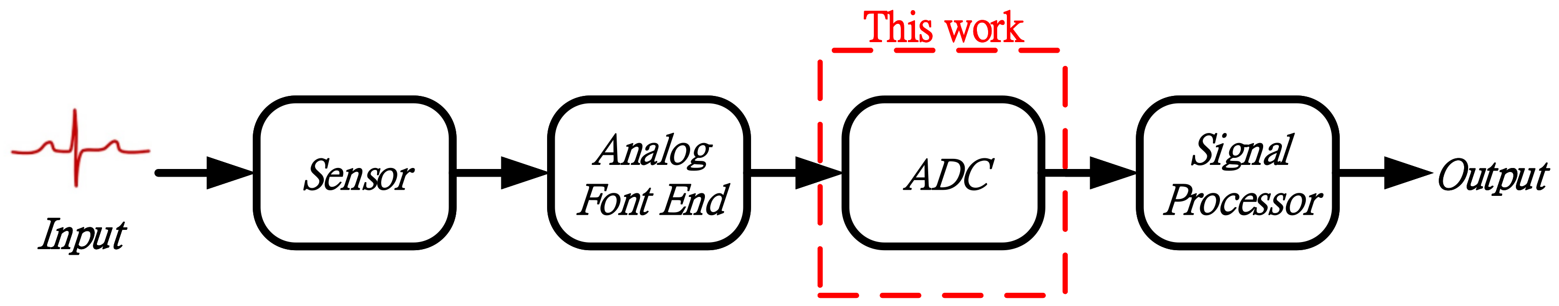
:1. Introduction
2. ADC Architecture for Biomedical Signal Detection
2.1. Delta-Sigma ADC
2.2. SAR ADC
2.3. Comparison of Differential Switch Capacitor Method
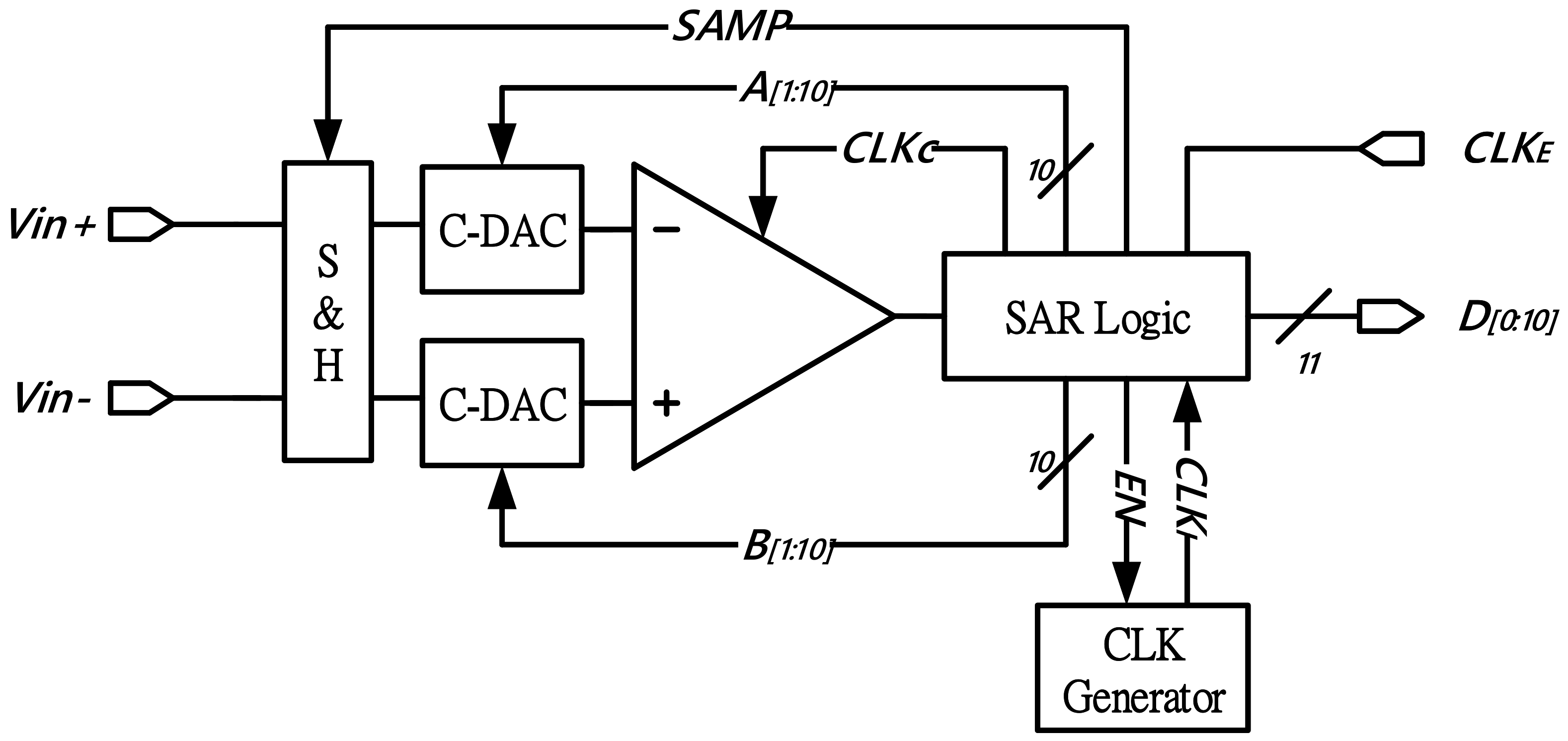
3. Proposed ADC Implementation
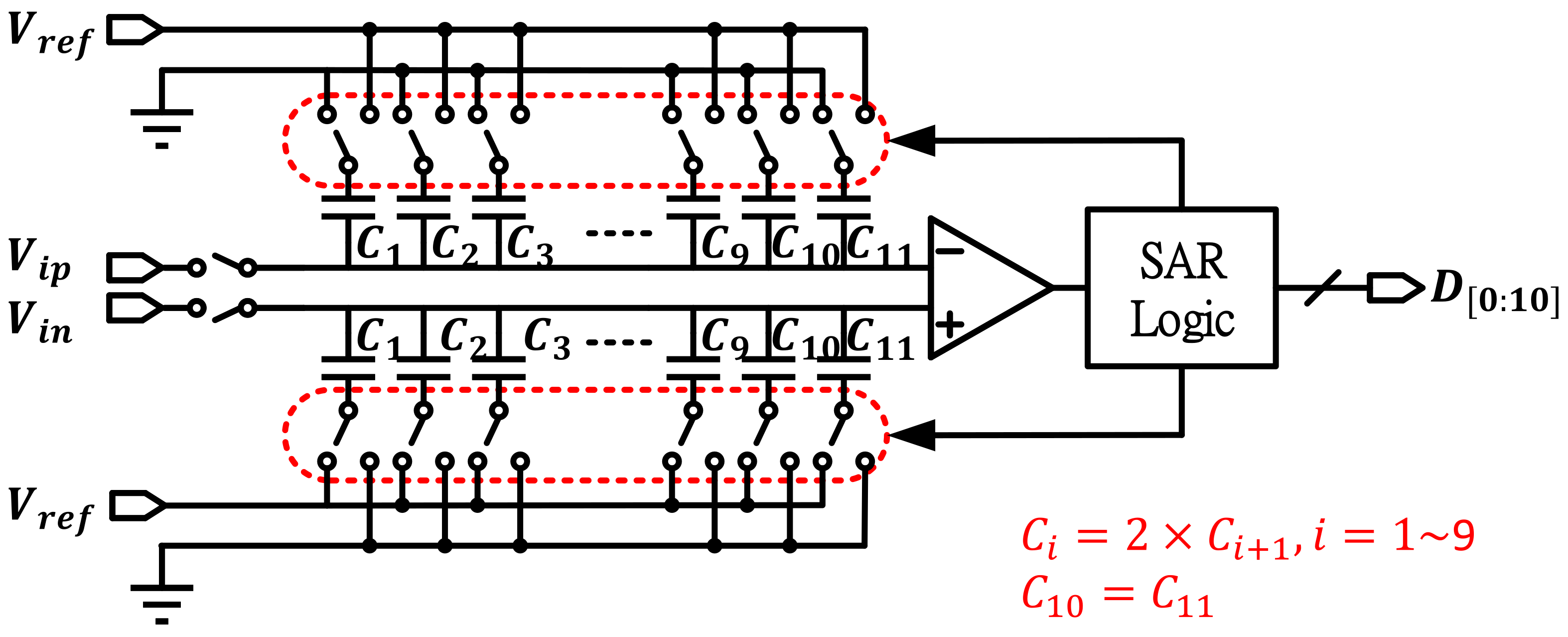
3.1. Capacitor Array
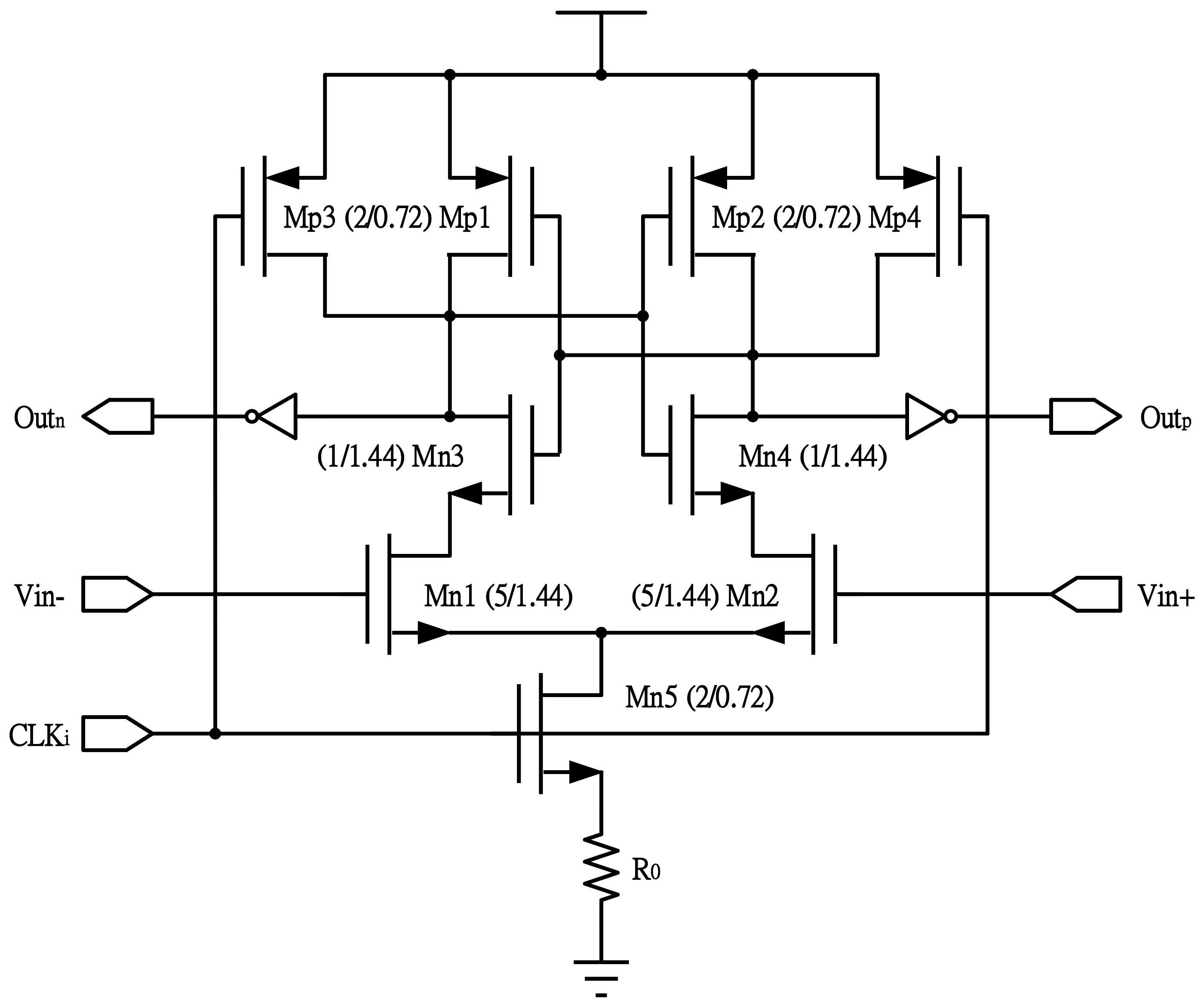
3.2. Comparator
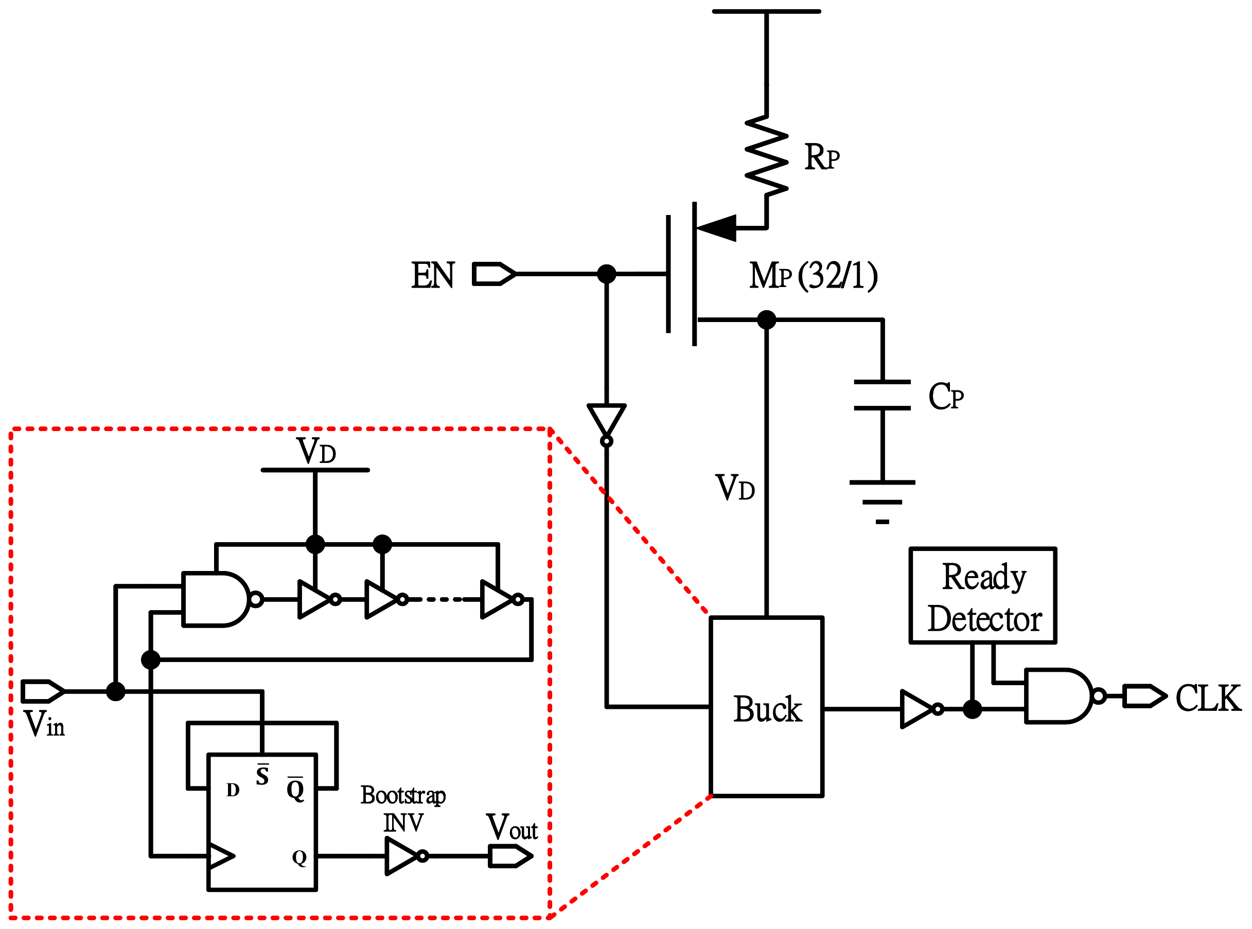
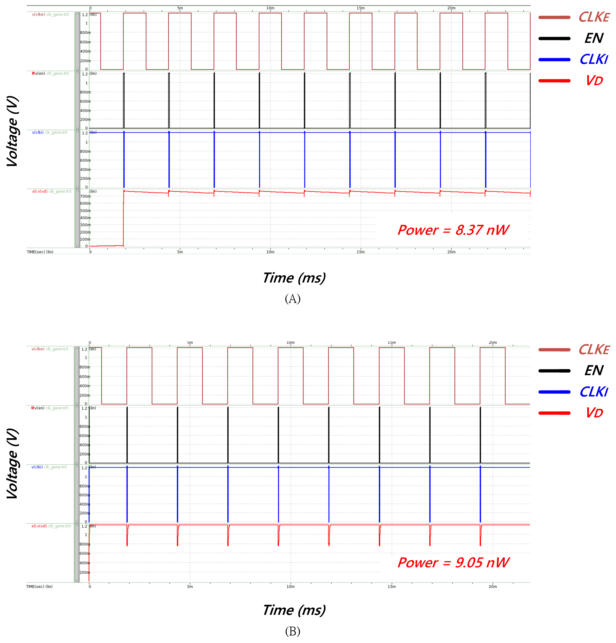
3.3. Clock Generator
3.4. Bootstrap Sample-and-Hold Circuit
4. Simulation and Measurement
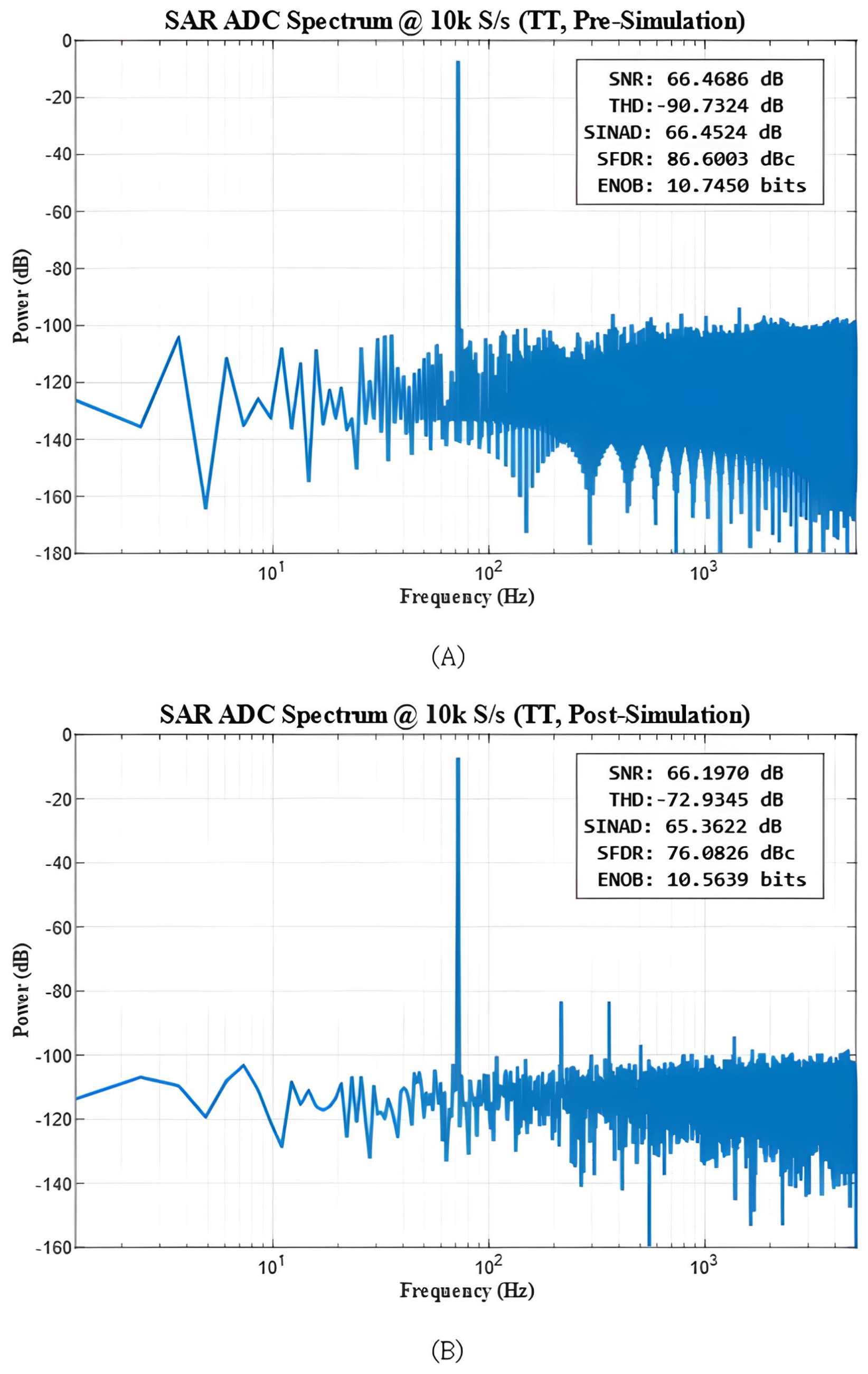
4.1. Simulation
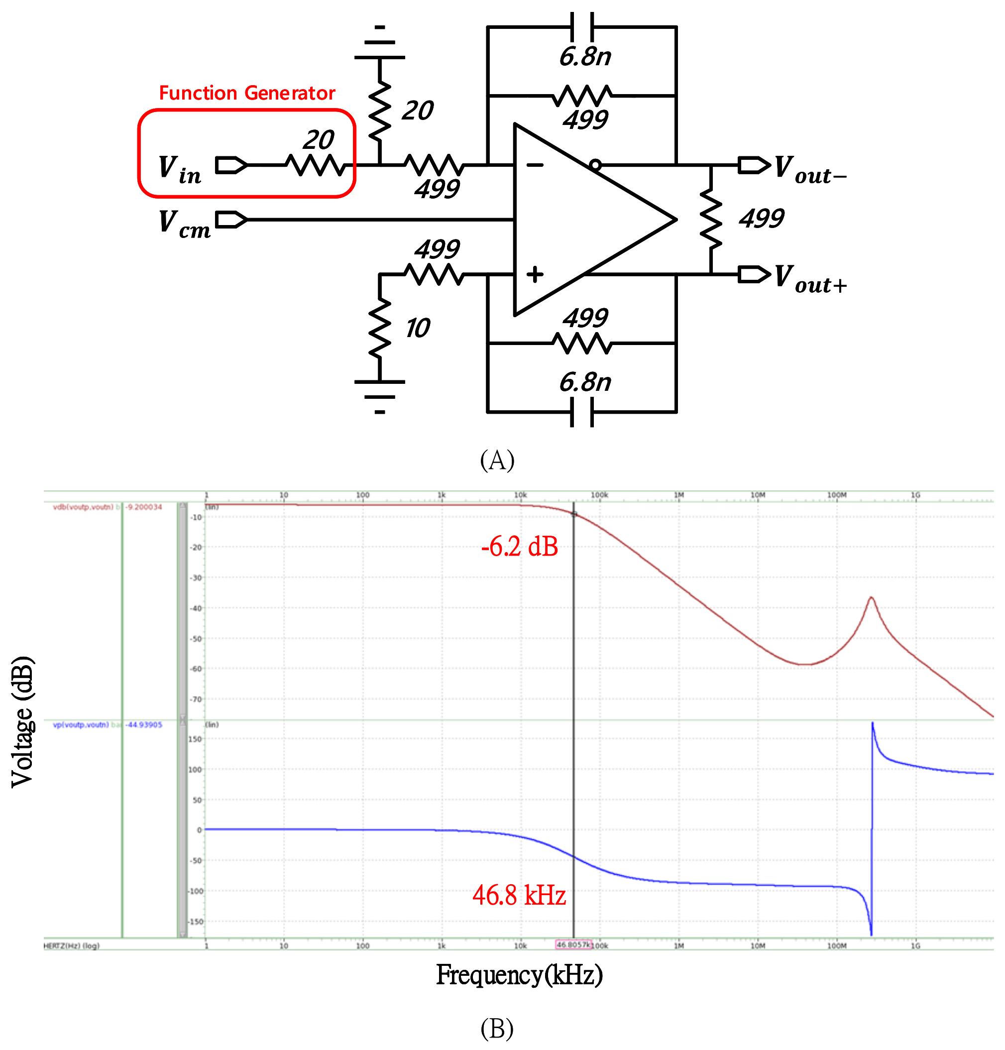
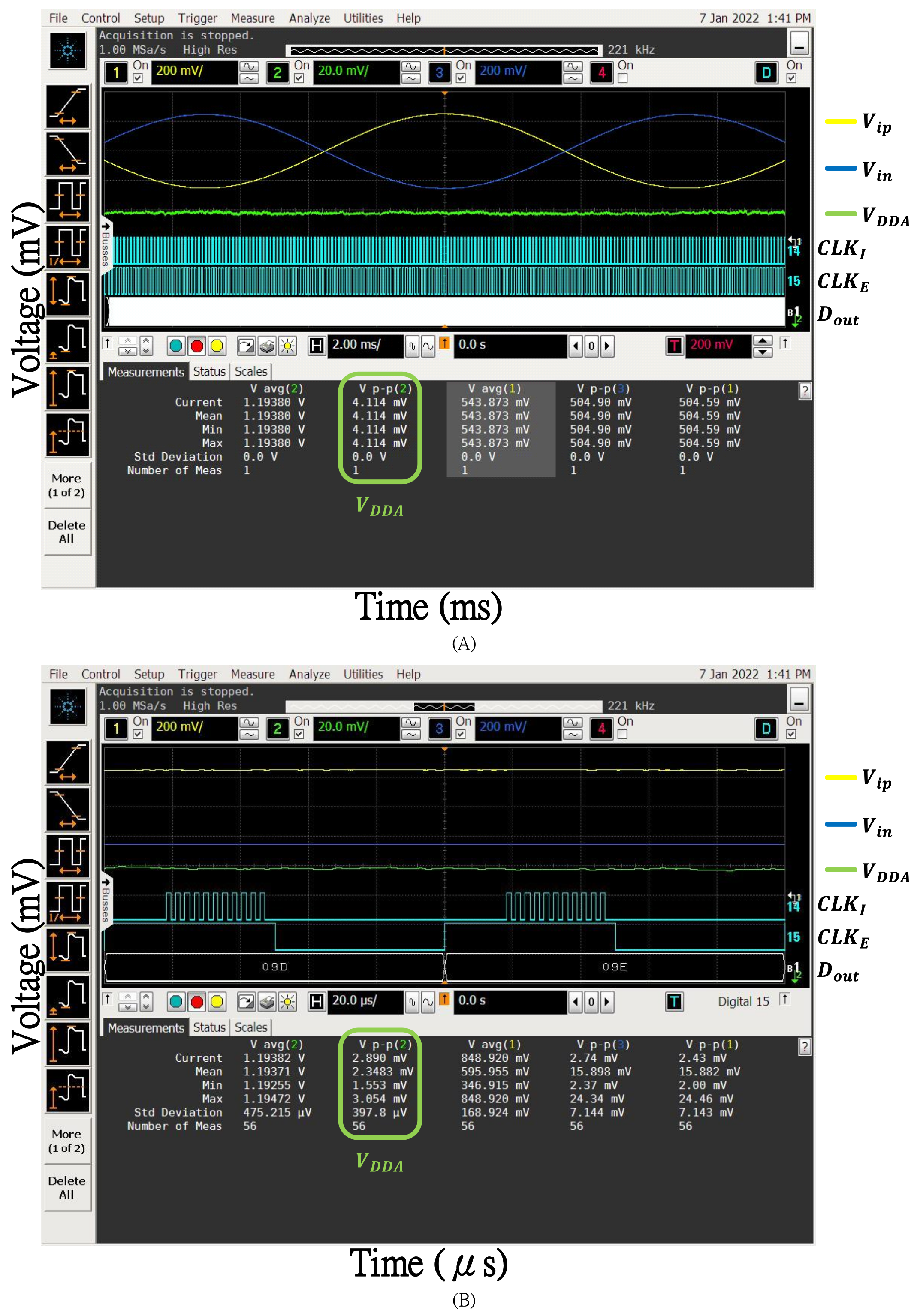
4.2. Measurement
5. Conclusions
Author Contributions
Funding
Data Availability Statement
Acknowledgments
Conflicts of Interest
References
- Yang, H.Y.; Sarpeshkar, R. A Bio-Inspired Ultra-Energy-Efficient Analog-to-Digital Converter for Biomedical Applications. IEEE Trans. Circuits Syst. I Regul. Pap. 2006, 53, 2349–2356. [Google Scholar] [CrossRef]
- Bonfanti, A.; Ceravolo, M.; Zambra, G.; Gusmeroli, R.; Borghi, T.; Spinelli, A.S.; Lacaita, A.L. A multi-channel low-power IC for neural spike recording with data compression and narrowband 400-MHz MC-FSK wireless transmission. In Proceedings of the European Conference on Solid-State Circuits (ESSCIRC), Seville, Spain, 14–16 September 2010; pp. 330–333. [Google Scholar]
- Markus, J.; Silva, J.; Temes, G.C. Theory and applications of incremental /spl Delta//spl Sigma/converters. IEEE Trans. Circuits Syst. I Regul. Pap. 2004, 51, 678–690. [Google Scholar] [CrossRef]
- Tan, Z.; Chen, C.H.; Chae, Y.; Temes, G.C. Incremental Delta-Sigma ADCs: A Tutorial Review. IEEE Trans. Circuits Syst. I Regul. Pap. 2020, 67, 4161–4173. [Google Scholar] [CrossRef]
- Hussain, J.; Usman, M.; Ramzan, R.; Saif, H. 12-bit Sigma-Delta Modulator for Biomedical Wireless Applications. In Proceedings of the International Conference on Open Source Systems and Technologies (ICOSST), Lahore, Pakistan, 15–16 December 2021; pp. 1–5. [Google Scholar]
- Devitha, P.S.; George, A. Design of Low Power High-Speed SAR ADC-A Review. In Proceedings of the International Conference on Computing Methodologies and Communication (ICCMC), Erode, India, 27–29 March 2019; pp. 864–868. [Google Scholar]
- Ginsburg, B.P.; Chandrakasan, A.P. An Energy-Efficient Charge Recycling Approach for A SAR Converter with Capacitive DAC. In Proceedings of the IEEE International Symposium on Circuits and Systems (ISCAS), Kobe, Japan, 23–26 May 2005; pp. 184–187. [Google Scholar]
- Liu, C.C.; Chang, S.J.; Huang, G.Y.; Lin, Y.Z. A 10-bit 50-MS/s SAR ADCwith a Monotonic Capacitor Switching Procedure. IEEE J. Solid-State Circuits 2010, 45, 731–740. [Google Scholar] [CrossRef]
- Lin, H.M.; Lin, C.H.; Wen, K.A. A Resolution-Reconfigurable and Power Scalable SAR ADC with Partially Thermometer Coded DAC. Adv. Sci. Technol. Eng. Syst. J. 2018, 3, 89–96. [Google Scholar] [CrossRef]
- Pang, W.Y.; Wang, C.S.; Chang, Y.K.; Chou, N.K.; Wang, C.K. A 10-bit 500-KSps low power SAR ADC with splitting comparator for bio-medical applications. In Proceedings of the IEEE Asian Solid-State Circuits Conference (A-SSCC), Taipei, Taiwan, 16–18 November 2009; pp. 149–152. [Google Scholar]
- Pelgrom, M.J.M.; Rens, A.C.J.v.; Vertregt, M.; Dijkstra, M.B. A 25-Ms/s 8-bit CMOS A/D converter for embedded application. IEEE J. Solid-State Circuits 1994, 29, 879–886. [Google Scholar] [CrossRef]
- Duan, J.; Jin, L.; Chen, D. A new method for estimating spectral performance of ADC from INL. In Proceedings of the IEEE International Test Conference (ITC), Austin, TX, USA, 2–4 November 2010; pp. 1–10. [Google Scholar]
- Figueiredo, P.M.; Vital, J.C. Low kickback noise techniques for CMOS latched comparators. In Proceedings of the IEEE International Symposium on Circuits and Systems (ISCAS), Vancouver, Canada, 23–26 May 2004; pp. 537–540. [Google Scholar]
- Li, Z.; Ma, Y.; Xie, Z. A Review of Improved CMOS Dynamic Comparators. In Proceedings of the IEEE International Conference on Electrical Engineering, Big Data and Algorithms (EEBDA), Changchun, China, 25–27 February 2022; pp. 734–741. [Google Scholar]
- Ho, Y.; Chang, C.; Su, C. Design of A Subthreshold-Supply Bootstrapped CMOS Inverter Based on An Active Leakage-Current Reduction Technique. IEEE Trans. Circuits Syst. II Express Briefs 2012, 59, 142–149. [Google Scholar] [CrossRef]
- Zhang, D.; Bhide, A.; Alvandpour, A. A 53-nW 9.1-ENOB 1-kS/s SAR ADC in 0.13-μm CMOS for Medical Implant Devices. IEEE J. -Solid-State Circuits 2012, 47, 1585–1593. [Google Scholar] [CrossRef]
- Kramer, M.J.; Janssen, E.; Doris, K.; Murmann, B. A 14 b 35 MS/s SAR ADC Achieving 75 dB SNDR and 99 dB SFDR with Loop-Embedded Input Buffer in 40 nm CMOS. IEEE J. -Solid-State Circuits 2015, 50, 142–149. [Google Scholar] [CrossRef]
- Zhang, D.; Alvandpour, A. A 12.5-ENOB 10-kS/s Redundant SAR ADC in 65-nm CMOS. IEEE Trans. Circuits Syst. II Express Briefs 2016, 63, 244–248. [Google Scholar] [CrossRef]
- Choi, S.; Ku, H.S.; Son, H.; Kim, B.; Park, H.J.; Sim, J.Y. An 84.6-dB-SNDR and 98.2-dB-SFDR Residue-Integrated SAR ADC for Low-Power Sensor Applications. IEEE J. -Solid-State Circuits 2018, 53, 404–417. [Google Scholar] [CrossRef]
- Mao, W.; Li, Y.; Heng, C.H.; Lian, Y. A Low Power 12-bit 1-kS/s SAR ADC for Biomedical Signal Processing. IEEE Trans. Circuits Syst. I Regul. Pap. 2019, 66, 477–488. [Google Scholar] [CrossRef]
- Hu, Y.; Chen, C.; Hu, L.; Huang, Q.; Tang, B.; Hu, M.; Yuan, B.; Wu, Z.; Li, B. A 9-10-Bit Adjustable and Energy-Efficient Switching Scheme for Successive Approximation Register Analog-to-Digital Converter with One Least Significant Bit Common-Mode Voltage Variation. Sensors 2024, 11, 3273. [Google Scholar] [CrossRef] [PubMed]


| fL(Hz) | fH(Hz) | CL(pF) | VSwing(V) | |
|---|---|---|---|---|
| Low Speed | 50 | 200 | 40 | 1.0 |
| High Speed | 1 | 5 K |
| Conventional | Vcm-Based | Monotonic | |
|---|---|---|---|
| No. of switches | 6 n + 2 | 6 n + 2 | 4 n + 2 |
| No. of capacitors | − 1 | ||
| Switching power | (2) | (3) | (4) |
| Pre-Simulation | Post-Simulation | |||||
|---|---|---|---|---|---|---|
| FF | TT | SS | FF | TT | SS | |
| (V) | 1.32 | 1.2 | 1.08 | 1.32 | 1.2 | 1.08 |
| Temp. (°C) | 0 | 25 | 80 | 0 | 25 | 80 |
| Input Freq. (Hz) | 72.02 | |||||
| (LSB) | 0.503 | 0.252 | 0.252 | 0.494 | 0.494 | 0.262 |
| (LSB) | 0.534 | 0.44 | 0.408 | 0.735 | 0.528 | 0.598 |
| THD (dB) | −77.44 | −90.73 | −82.6 | −74.67 | −72.93 | −76.74 |
| SNR (dB) | 66.49 | 66.47 | 66.48 | 66.28 | 66.2 | 66.17 |
| SFDR (dBc) | 77.84 | 86.6 | 83.14 | 76.25 | 76.08 | 77.61 |
| SINAD (dB) | 66.16 | 66.45 | 66.38 | 65.69 | 65.36 | 65.81 |
| ENOB (Bits) | 10.7 | 10.75 | 10.73 | 10.62 | 10.56 | 10.64 |
| [16] | [17] | [18] | [19] | [20] | [21] | This Work | ||
|---|---|---|---|---|---|---|---|---|
| (V) | 1.0 | 0.6 | 0.8 | 1.8 | 1.0 | 1.0 | 1.2 | |
| CLK Mode | Syn. | Asyn. | Syn. | Asyn. | Syn. | Syn. | Asyn. | |
| Technology (nm) | 130 | 65 | 65 | 180 | 130 | 180 | 180 | |
| Sampling Rate (Hz) | 1 K | 500 | 10 K | 2 K | 10 K | 100 K | 400 | 10 K |
| Resolution (Bits) | 10 | 8 | 14 | 16 | 12 | 10 | 11 | |
| (LSB) | 0.61 | 1.0 | 2.2 | 0.7 | 0.41 | 0.33 | 0.256 | |
| (LSB) | 0.46 | 1.8 | 2.2 | 3.65 | 0.74 | 0.25 | 0.459 | |
| SFDR (dBc) | 67.6 | - | 88.8 | 98.2 | 64.8 | 54.14 | 72.2 | 78.9 |
| ENOB (Bits) | 9.13 | 7.14 | 12.5 | 13.8 | 10.5 | 8.84 | 9.27 | 9.2 |
| Power (W) | 53 n | 1.8 n | 1.98 | 7.93 | 110 n | 0.67 | 36.5 n | 932 n |
Disclaimer/Publisher’s Note: The statements, opinions and data contained in all publications are solely those of the individual author(s) and contributor(s) and not of MDPI and/or the editor(s). MDPI and/or the editor(s) disclaim responsibility for any injury to people or property resulting from any ideas, methods, instructions or products referred to in the content. |
© 2024 by the authors. Licensee MDPI, Basel, Switzerland. This article is an open access article distributed under the terms and conditions of the Creative Commons Attribution (CC BY) license (https://creativecommons.org/licenses/by/4.0/).
Share and Cite
Shiue, M.-T.; Lo, Y.-F.; Jung, C.-Y. Design of an Internal Asynchronous 11-Bit SAR ADC for Biomedical Wearable Application. Electronics 2024, 13, 3549. https://doi.org/10.3390/electronics13173549
Shiue M-T, Lo Y-F, Jung C-Y. Design of an Internal Asynchronous 11-Bit SAR ADC for Biomedical Wearable Application. Electronics. 2024; 13(17):3549. https://doi.org/10.3390/electronics13173549
Chicago/Turabian StyleShiue, Muh-Tian, Yu-Fan Lo, and Chih-Yao Jung. 2024. "Design of an Internal Asynchronous 11-Bit SAR ADC for Biomedical Wearable Application" Electronics 13, no. 17: 3549. https://doi.org/10.3390/electronics13173549
APA StyleShiue, M.-T., Lo, Y.-F., & Jung, C.-Y. (2024). Design of an Internal Asynchronous 11-Bit SAR ADC for Biomedical Wearable Application. Electronics, 13(17), 3549. https://doi.org/10.3390/electronics13173549