Article

A Novel Modular Multilevel Converter Topology with High- and Low-Frequency Modules and Its Modulation Strategy

1
National Engineering Research Center for Electrical Energy Conversion and Control, Hunan University, Changsha 410082, China
2
Electric Power Research Institute, China Southern Power Grid (SGCC), Guangzhou 510000, China
*
Author to whom correspondence should be addressed.
Electronics 2024, 13(18), 3656; https://doi.org/10.3390/electronics13183656
Submission received: 4 August 2024 / Revised: 29 August 2024 / Accepted: 11 September 2024 / Published: 13 September 2024

Abstract

:
To resolve the issue of the difficultly in effectively balancing the output performance improvement, cost reduction, and efficiency improvement of a medium-voltage modular multilevel converter (MMC), a novel MMC (NMMC) topology based on high- and low-frequency hybrid modulation is proposed in this study. Each arm of the NMMC contains a high-frequency sub-module composed of a heterogeneous cross-connect module (HCCM) and N − 1 low-frequency sub-modules composed of half-bridge converters. The high-frequency bridge arm of the HCCM in this study adopts SiC MOSFET devices, while the commutation bridge arm and low-frequency sub-module of the HCCM adopt Si IGBT devices. For the NMMC topology, this study adopts a high/low-frequency hybrid modulation strategy, which gives full play to the advantages of low switching loss in SiC MOSFET devices and low on-state loss in Si IGBT devices. In addition, a specific capacitor voltage balance strategy is proposed for the HCCM, and the working state of the HCCM is analyzed in detail. Furthermore, the feasibility and effectiveness of the proposed topology, modulation strategy, and voltage balancing strategy are verified by experiments. Finally, the proposed topology is compared with the existing MMC topology in terms of device cost and operating loss, which proves that the proposed topology can better balance the cost and efficiency indicators of the device.

1. Introduction

Modular multilevel converters (MMCs) are widely used in locomotive traction, new energy grid connections, power quality control, and other medium-voltage fields due to its strong scalability and good redundancy [1,2,3,4]. The number of sub-modules in the MMC in medium-voltage applications is relatively small. The number of levels and the equivalent switching frequency of the MMC become the key factors restricting the improvement in its output performance. Recently, relevant scholars have improved the output performance of medium-voltage MMCs from the perspectives of modulation optimization, topology optimization, and new device applications [5,6,7,8].
In terms of MMC modulation strategy, the most commonly used modulation strategies are nearest-level modulation (NLM) and carrier phase shift pulse width modulation (CPS-PWM) [9,10,11]. NLM has the advantages of simple regulation and low-switching frequency, but it can only output N + 1 levels, and the low-order harmonic content is higher under the condition of fewer modules. To this end, ref. [12] proposed an improved NLM strategy with 2N + 1 levels. By changing the set value of the NLM selection function, the time of the upper and lower arm level change is staggered, and the output levels of the MMC are increased from N + 1 to 2N + 1. On this basis, ref. [13] reduced the amplitude of MMC output harmonics and capacitor voltage fluctuations by adding a small offset to the reference signal. Although the improved NLM algorithm can improve the output performance of the MMC, its equivalent output switching frequency is low and the low-order harmonic content is still high. Compared with NLM, CPS-PWM has a high equivalent switching frequency and good waveform quality and can output 2N + 1 levels, but the working frequency of each module is high and the overall switching loss is large. Therefore, it is difficult to solve the problem of optimizing output performance and operating efficiency via the existing single-modulation strategy and optimization method.
To further improve the output performance of an MMC, scholars have carried out relevant work from the aspects of modulation mixing and device mixing. Therefore, a nearest-level PWM (NLM-PWM) strategy is proposed in [14,15]. The modulation strategy only requires one high-frequency sub-module to output a PWM wave, while the remaining sub-modules adopt NLM strategy, and can achieve similar output performance to CPS-PWM. Similarly, refs. [16,17] proposed an MMC topology with an additional full-bridge auxiliary module per bridge arm, which can output 2N + 3 levels combined with the NLM-PWM strategy. However, the equivalent output frequency of the NLM-PWM strategy is equal to the switching frequency of the high-frequency sub-module, and the specific position of the high-frequency sub-module in the bridge arm is determined by the operating state, which would change randomly in the bridge arm. Therefore, in order to improve the equivalent output frequency of MMC, the switching performance of the whole device is required to be higher. To this end, ref. [18] further optimized the hybrid modulation strategy and fixed the high-frequency modulation in several half-bridge sub-modules based on SiC MOSFET devices, while the remaining half-bridge sub-modules used half-bridge modules based on Si IGBT devices. The wide-band-gap semiconductor devices represented by SiC MOSFET have better performance in switching frequency and thermal conductivity [19,20], so the efficiency of the whole hybrid scheme is higher, but the cost of SiC devices is high [21], and the cost of the whole device is higher. Furthermore, ref. [22] proposes to fix the high-frequency action of each bridge arm to two full-bridge submodules based on SiC MOSFET devices. The topology can output 2N + 1 levels and the breakdown voltage of SiC MOSFET devices is doubled. However, each bridge arm contains two full-bridge SiC MOSFET devices, the number of SiC MOSFET devices is large, and the overall cost is still high. Compared with SiC devices, GaN devices have higher switching frequency and smaller switching loss, so they have attracted much attention in high-frequency applications. References [23,24] proposed a GaN-based MMC topology and experimentally demonstrated that its efficiency can reach 98.9%. In reference [25], the advantages and disadvantages of SiC MMC and GaN MMC are compared in detail. Therefore, the hybrid topology of GaN and Si IGBT devices will also be a way to improve the comprehensive index of the converter.
Aiming at the issue that it is difficult to effectively balance the output performance, cost reduction, and efficiency improvement of large-capacity devices, a novel MMC (NMMC) topology based on a hybrid modulation strategy is proposed. Firstly, the topological structure of the NMMC is introduced, and its corresponding modulation strategy and modulation mode are analyzed. Then, the energy fluctuation mechanism of high-frequency sub-modules under each modulation mode is quantitatively analyzed. Furthermore, the working state of the high-frequency sub-module under two modulation modes is analyzed in detail, and the voltage equalization process is given. The availability of the proposed NMMC topology, modulation strategy, and voltage balancing method is proved by experiments. Finally, a comprehensive comparison is made between the proposed topology and the existing topology in terms of cost and loss to prove the performance advantage of the proposed NMMC.

2. Topological Structure of NMMC

The proposed topology is shown in Figure 1. This structure is similar to the traditional MMC, and the upper and lower arms are completely symmetrical. Each bridge arm is composed of a high-frequency sub-module (HFSM), N − 1 low-frequency sub-modules (LFSMs) and a bridge arm inductance in series. Among them, the LFSMs adopt the traditional half-bridge converter based on Si IGBT devices; for high-frequency sub-modules, this study proposes a heterogeneous cross-connected module (HCCM). The HCCM consists of two half-bridge submodules (HSM11, HSM12), which are cross-connected by the commutation bridge arm. It consists of four SiC MOSFET devices, two Si IGBT devices and two capacitors. The withstand voltage of SiC MOSFET devices in the proposed HCCM is only half of that of Si IGBT devices. CH1 and CH2 are the DC capacitance of the HCCM, and CL and L are the DC capacitance of the LFSM and the bridge arm inductance, respectively. uao, ubo, and uco are the three-phase output voltages of the NMMC. Udc is the DC-side voltage of NMMC, Uc is the DC-side capacitor voltage of LFSM, and Uc1 and Uc2 are the DC capacitor voltages of the HCCM (Uc1= Uc2 = Uc/2).

3. Hybrid Modulation Strategy of the NMMC

In the proposed NMMC modulation strategy the LFSMs use NLM to output the power frequency step wave, and the high-frequency sub-module uses unipolar PWM to output the high-frequency pulse.

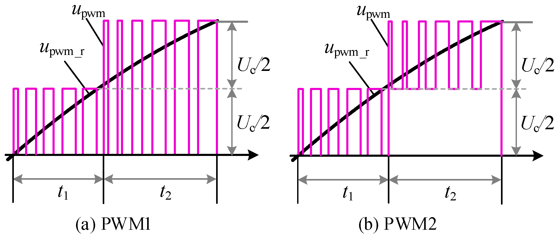
3.1. The Hybrid Modulation Principle of the NMMC

Taking the phase a upper bridge arm as an example, since the HCCM can output positive and negative symmetrical high-frequency PWM waves, the hybrid modulation strategy will have two operating conditions. In this study, the following definition is made: when the HCCM outputs a positive PWM wave, it is using modulation mode I; when the HCCM outputs a negative PWM wave, it is using modulation mode II.
For mode I, the HCCM outputs a positive PWM wave, and the equivalent modulation principle is shown in Figure 2. The upper bridge arm voltage uao_p is composed of two parts: one is the step wave voltage ustep_pa output by the LFSMs, and the other is the high-frequency shaping pulse upwm_pa output by the HCCM.
The output voltage of the NMMC is defined as
u ao = U m cos ( ω t )
where ω and Um are the angular frequency and the output voltage amplitude, respectively. If the modulation factor is defined as m, then
U m = m × N 2 U c
According to the mathematical model of MMC, the modulation reference wave of the upper arm can be written as
u ao _ pr = N 2 U c N 2 U c m cos ( ω t )
From (3), the sub-modules number that need to be inserted in the LFSMs of the upper bridge arm is
n step _ pa = f l o o r ( u ao _ pr / U c )
where floor(x) is a down-integer function.
Therefore, the modulating wave of the HCCM of the bridge arm on phase a is
u pwm _ par = u ao _ pr U c f l o o r ( u ao _ pr / U c )
For mode II, the HCCM outputs a negative PWM wave, and the equivalent modulation principle is shown in Figure 2b. Compared with mode I, the step-wave voltage of the low-frequency sub-module in mode II can be expressed as
u step _ pa = u step _ pa + U c
Therefore, mode II needs to invest one more low-frequency sub-module than mode I, so the number of sub-modules that need to be invested in the LFSMs of the bridge arm on phase a is
n step _ pa = f l o o r ( u ao _ pr / U c ) + 1
In mode II, the modulating wave of the HCCM of the bridge arm on phase a is
u pwm _ par = u ao _ pa U c f l o o r ( u ao _ pr / U c ) U c
In summary, both modulation modes focus the high-frequency switching action on the SiC MOSFET devices in the HCCM, while the LFSMs composed of Si IGBTs are only responsible for outputting low-frequency step waves. Therefore, the scheme gives full play to the advantages of low switching loss in the SiC MOSFET devices and low conduction loss in the Si IGBT devices in high-power and high-current scenarios. It can greatly decrease the overall operating loss in the devices and enhance the efficiency of the devices.

3.2. Modulation Principle of HCCM

The HCCM can output five levels: Uc, Uc/2, 0, −Uc/2, −Uc. The switching mode of the HCCM is shown in Table 1. It can be seen from Table 1 that the commutation bridge arm (i.e., the branch of the Si IGBT device) is the fundamental frequency switching period, so the Si IGBT devices with low switching frequency and low on-state loss is adopted. If the HCCM is modulated by high-frequency PWM, then T1 to T4 operate in a high-frequency switching state. If the HCCM adopts high-frequency PWM, T1 to T4 work in high-frequency switching state, so SiC MOSFET devices with low switching loss is adopted.
When the HCCM uses PWM, there will be two modulation results, as shown in Figure 3. Among them, upwm_r is the modulation wave, and upwm is the output voltage of HCCM. For t1 stage, 0 < upwm_r < Uc/2, one HSM in HCCM is bypassed, and the other HSM outputs a PWM wave. For the t2 stage, upwm_r > Uc/2, there will be two PWM cases. One case is that HSM11 and HSM12 cooperate to output PWM waves with an amplitude of 0 to Uc, as shown in Figure 3a. Another case is that one HSM is normally connected and the other HSM outputs a PWM wave, then the equivalent output of HCCM is a PWM wave from Uc/2 to Uc, as shown in Figure 3b. By comparison, it can be seen that the modulation result corresponding to Figure 3b is closer to the modulation wave, so this study takes it as the PWM method of HCCM.

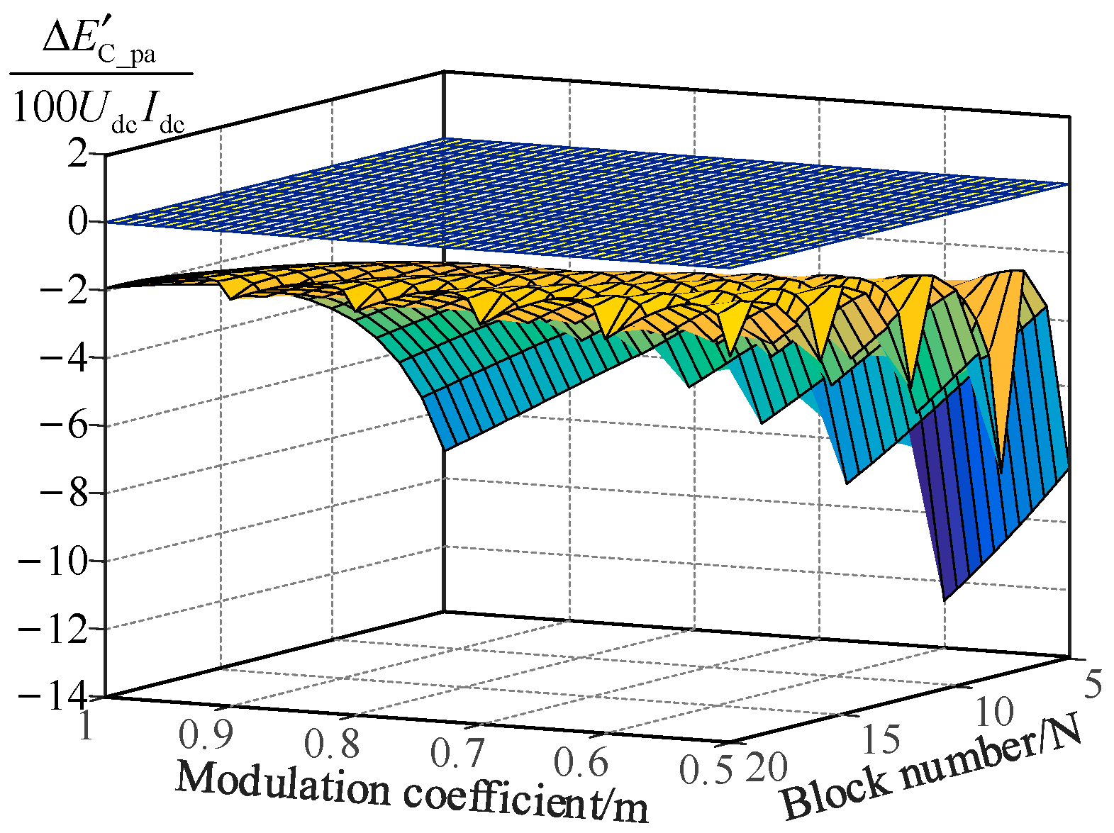
4. Capacitor Energy Analysis of the HCCM

The LFSMs in the proposed NMMC can achieve voltage stabilization by using the traditional sorting voltage equalization algorithm [14], which will not be repeated in this paper. The HCCM’s inability to contribute to voltage balancing with low-frequency sub-modules stems from the constant output of high-frequency PWM waves, leaving the energy variation of the DC capacitor unpredictable. Taking the HCCM of the bridge arm on phase a as an example, the energy fluctuation mechanism is analyzed as follows.
In mode I, it can be seen from (3) and (5) that the average switching function of the HCCM is
S pa = N 2 N 2 m cos ( ω t ) f l o o r ( N 2 N 2 m cos ( ω t ) )
Neglecting the effect of circulating current, the bridge arm current can be expressed due to the conservation of power between the AC and DC sides.
i arm _ pa = I dc 3 1 + 2 m cos φ cos ( ω t + φ )
where φ is the load power factor angle.
Combining (9) and (10), the expression of the total energy fluctuation of the DC capacitor of the HCCM on the upper arm can be obtained as follows
Δ E C _ pa = 0 2 π U dc N S pa i arm _ pa d ( ω t )
In mode II, the average switching function of the HCCM on the upper arm can be expressed as
S pa = S pa 1
Since the expressions of the bridge arm voltage and current are unchanged, the total energy variation in the DC-side capacitor of HCCM in mode II is expressed as
Δ E C _ pa = 0 2 π U dc N S pa i arm _ pa d ( ω t )
Suppose that φ = 0, the sketches of Δ E C _ pa and Δ E C _ pa in MATLAB are shown in Figure 4 and Figure 5. It can be seen that Δ E C _ pa is greater than 0 in the range of N and m, and the fluctuation amplitude of Δ E C _ up increases with the decrease in the number of modules. Therefore, in mode I, the capacitor voltage of the HCCM will always increase. The value of Δ E C _ pa is less than 0 in the range of N and m, and the fluctuation amplitude of Δ E C _ pa increases with the decrease in the number of modules. Therefore, in mode II, the capacitor voltage of the HCCM will always decrease.
Therefore, by controlling the low-frequency switching of the NMMC between mode I and mode II, the state of charge and discharge of the HCCM’s DC capacitor can be adjusted in order to sustain equilibrium in the overall capacitor energy within the HCCM.

5. The Voltage Balancing Strategy of NMMC

5.1. Internal Balance of Two Capacitor Voltages in HCCM

The HCCM can output five levels: Uc, Uc/2, 0, −Uc/2, and −Uc. When S1 is disconnected and S2 is turned on, the HCCM outputs a positive PWM pulse, corresponding to mode I. When S1 is turned on and S2 is disconnected, the HCCM outputs a negative PWM pulse, corresponding to mode II. According to the output PWM polarity of the HCCM and the current direction of the bridge arm, the eight working states corresponding to each mode are shown in Figure 6 and Figure 7. The specific analysis of the operating state of the HCCM DC capacitor corresponding to each operating mode is as follows:
I(a): When the bridge arm current iarm > 0, S1 is deactivated and S2 is activated. T1 and T4 are switched on, while T2 and T3 are switched off. The voltage upwm equals Uc, and CH1 and CH2 are both in the charging state.
I(b): When the bridge arm current iarm > 0, S1 is deactivated and S2 is activated. T2 and T4 are switched on, while T1 and T3 are switched off. The voltage upwm equals Uc/2, and CH1 is in the bypass state, while CH2 is in the charging state.
I(c): When the bridge arm current iarm > 0, S1 is deactivated and S2 is activated. T1 and T3 are switched on, while T2 and T4 are switched off. The voltage upwm equals Uc/2, and CH2 is in the bypass state, while CH1 is in the charging state.
I(d): When the bridge arm current iarm > 0, S1 is deactivated and S2 is activated. T2 and T3 are switched on, while T1 and T4 are switched off. The voltage upwm equals 0, and CH1 and CH2 are both in the bypass state.
I(e): When the bridge arm current iarm < 0, S1 is deactivated and S2 is activated. T1 and T4 are switched on, while T2 and T3 are switched off. The voltage upwm equals Uc, and CH1 and CH2 are both in the discharging state.
I(f): When the bridge arm current iarm < 0, S1 is deactivated and S2 is activated. T2 and T4 are switched on, while T1 and T3 are switched off. The voltage upwm equals Uc/2, and CH1 is in the bypass state, while CH2 is in the discharging state.
I(g): When the bridge arm current iarm < 0, S1 is deactivated and S2 is activated. T1 and T3 are switched on, while T2 and T4 are switched off. The voltage upwm equals Uc/2, and CH2 is in the bypass state, while CH1 is in the discharging state.
I(h): When the bridge arm current iarm < 0, S1 is deactivated and S2 is activated. T2 and T3 are switched on, while T1 and T4 are switched off. The voltage upwm equals 0, and CH1 and CH2 are both in the bypass state.
II(a): When the bridge arm current iarm > 0, S2 is deactivated and S1 is activated. T2 and T3 are turned on, while T1 and T4 are turned off. The voltage upwm equals −Uc, and CH1 and CH2 are both in the discharging state.
II(b): When the bridge arm current iarm > 0, S2 is deactivated and S1 is activated. T1 and T3 are turned on, while T2 and T4 are turned off. The voltage upwm equals −Uc/2, and CH1 is in the bypass state, while CH2 is in the discharging state.
II(c): When the bridge arm current iarm > 0, S2 is deactivated and S1 is activated. T2 and T4 are turned on, while T1 and T3 are turned off. The voltage upwm equals −Uc/2, and CH2 is in the bypass state, while CH1 is in the discharging state.
II(d): When the bridge arm current iarm > 0, S2 is deactivated and S1 is activated. T1 and T4 are turned on, while T2 and T3 are turned off. The voltage upwm equals 0, and CH1 and CH2 are both in the bypass state.
II(e): When the bridge arm current iarm < 0, S2 is deactivated and S1 is activated. T2 and T3 are turned on, while T1 and T4 are turned off. The voltage upwm equals −Uc, and CH1 and CH2 are both in the charging state.
II(f): When the bridge arm current iarm < 0, S2 is deactivated and S1 is activated. T1 and T3 are turned on, while T2 and T4 are turned off. The voltage upwm equals −Uc/2, and CH1 is in the bypass state, while CH2 is in the charging state.
II(g): When the bridge arm current iarm < 0, S2 is deactivated and S1 is activated. T2 and T4 are turned on, while T1 and T3 are turned off. The voltage upwm equals −Uc/2, and CH2 is in the bypass state, while CH1 is in the charging state.
II(h): When the bridge arm current iarm < 0, S2 is deactivated and S1 is activated. T1 and T4 are turned on, while T2 and T3 are turned off. The voltage upwm equals 0, and CH1 and CH2 are both in the bypass state.
Therefore, by controlling the high-frequency sub-module to switch flexibly between 16 working states, the charging and discharging states of the two DC capacitors CH1 and CH2 in the HCCM can be changed to achieve the internal balance of the two capacitor voltages.

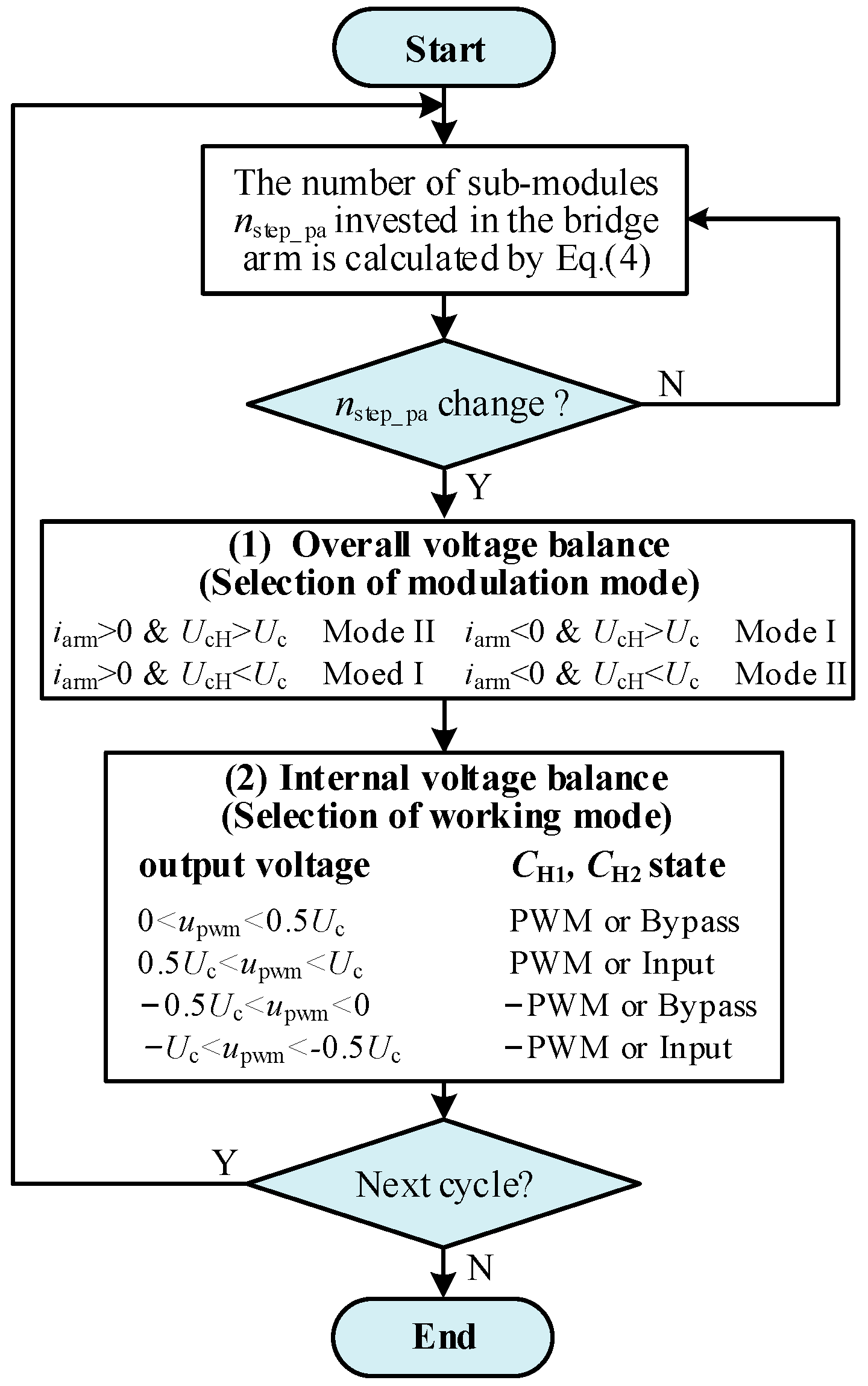
5.2. Voltage Balance Process of the HCCM

Taking the phase a upper bridge arm as an example, the high-frequency sub-module voltage balance mainly includes two blocks: overall voltage balance and internal voltage balance. The specific voltage equalization process is shown in Figure 8. Among them, UcH is the sum of two DC capacitor voltages of the high-frequency sub-module.
(1)
The number of nstep_pa needed to be put into the low-frequency sub-module of the upper bridge arm is calculated by (4).
(2)
The current time is compared with the nstep_pa calculated at the previous time. If there is no change, it is recalculated. If it changes, it enters the process of voltage balance.
(3)
Overall voltage balance. If iarm > 0 and nstep_pa = N − 1, it can only work in mode I. If iarm > 0 and nstep_pa < N − 1, the relationship between the total capacitor voltage UcH of the high-frequency sub-module and the reference capacitor voltage Uc is judged. If UcH < Uc, it works in mode I; if UcH > Uc, it works in mode II. If iarm< 0 and nstep_pa = N − 1, then it can only work in mode I. If iarm < 0 and nstep_pa < N − 1, the relationship between the capacitor voltage of the high-frequency sub-module and the reference capacitor voltage Uc is judged. If UcH < Uc, it works in mode II; if UCH > Uc, it works in mode I.
(4)
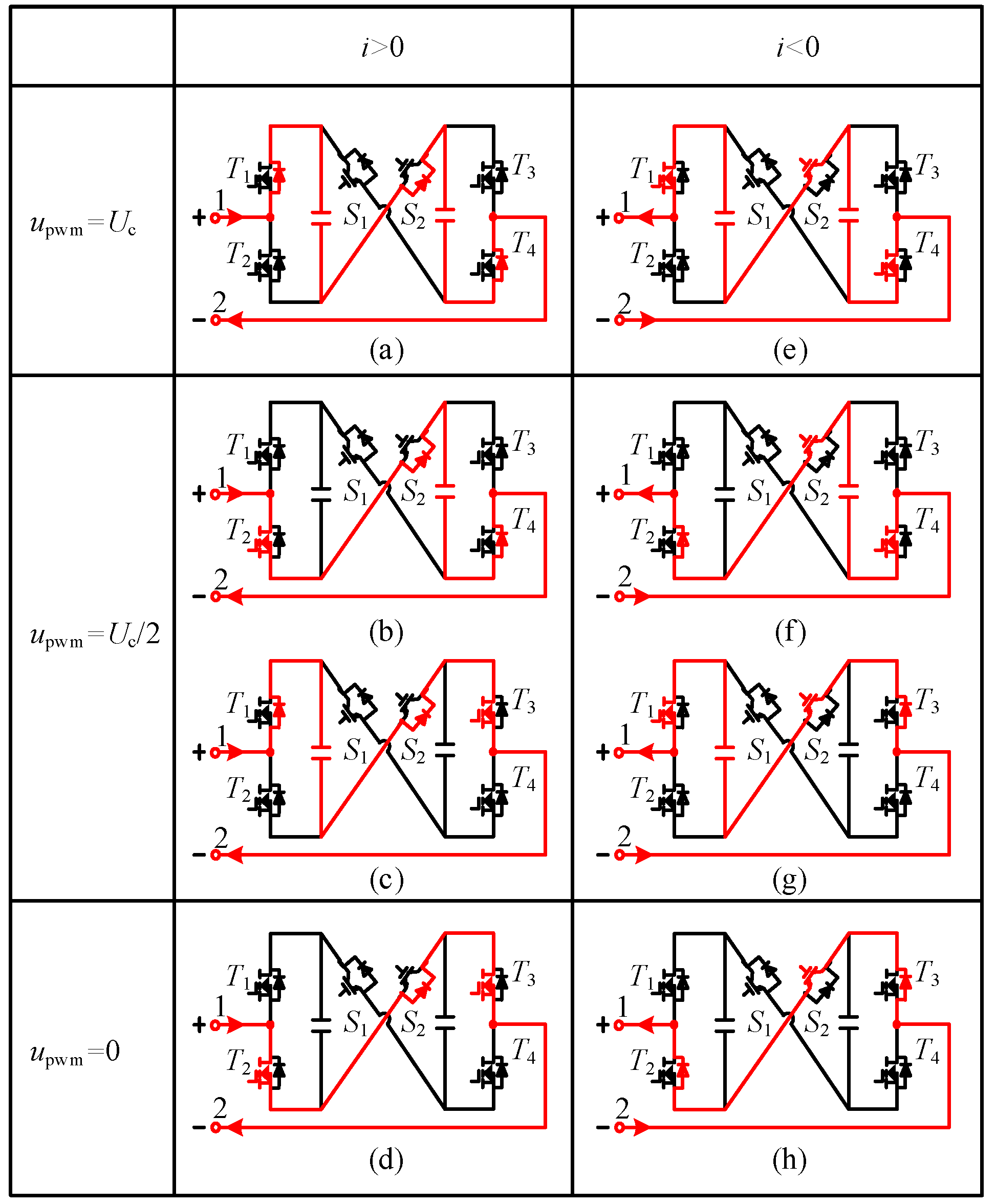
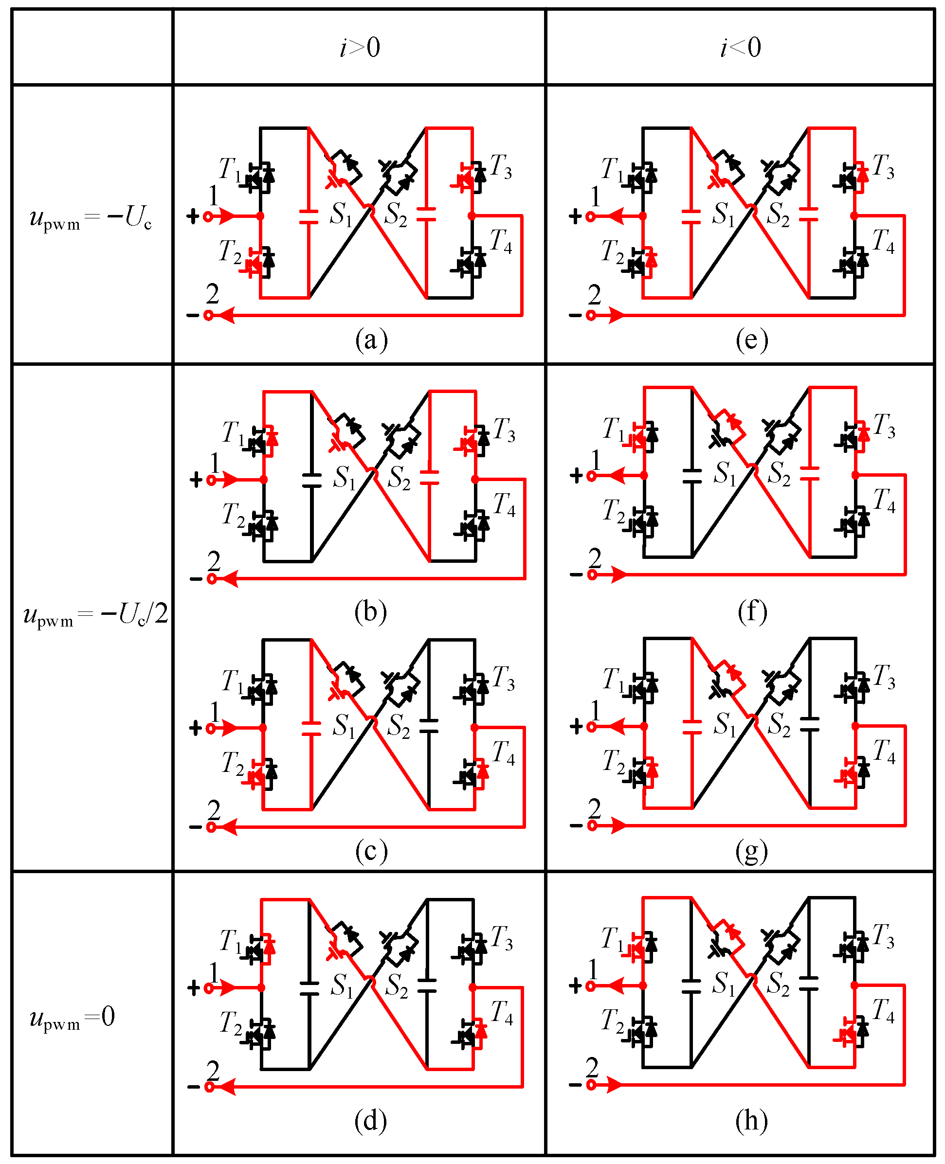
Internal voltage balance. Taking the output positive voltage of the high-frequency sub-module as an example, upwm = Uc and iarm > 0, the high-frequency sub-module is charged as a whole, and the capacitor CH1 and CH2 with a small voltage are directly input, and the capacitor with a high voltage outputs PWM; upwm = Uc and iarm < 0, the high-frequency sub-module is charged as a whole, and the high-voltage capacitors CH1 and CH2 are bypassed, and the low-voltage capacitors output PWM; when upwm= 0.5Uc and iarm < 0, the high-frequency sub-module is discharged as a whole, then the capacitor CH1 and CH2 with a small voltage are bypassed, and the capacitor with a high voltage outputs PWM.

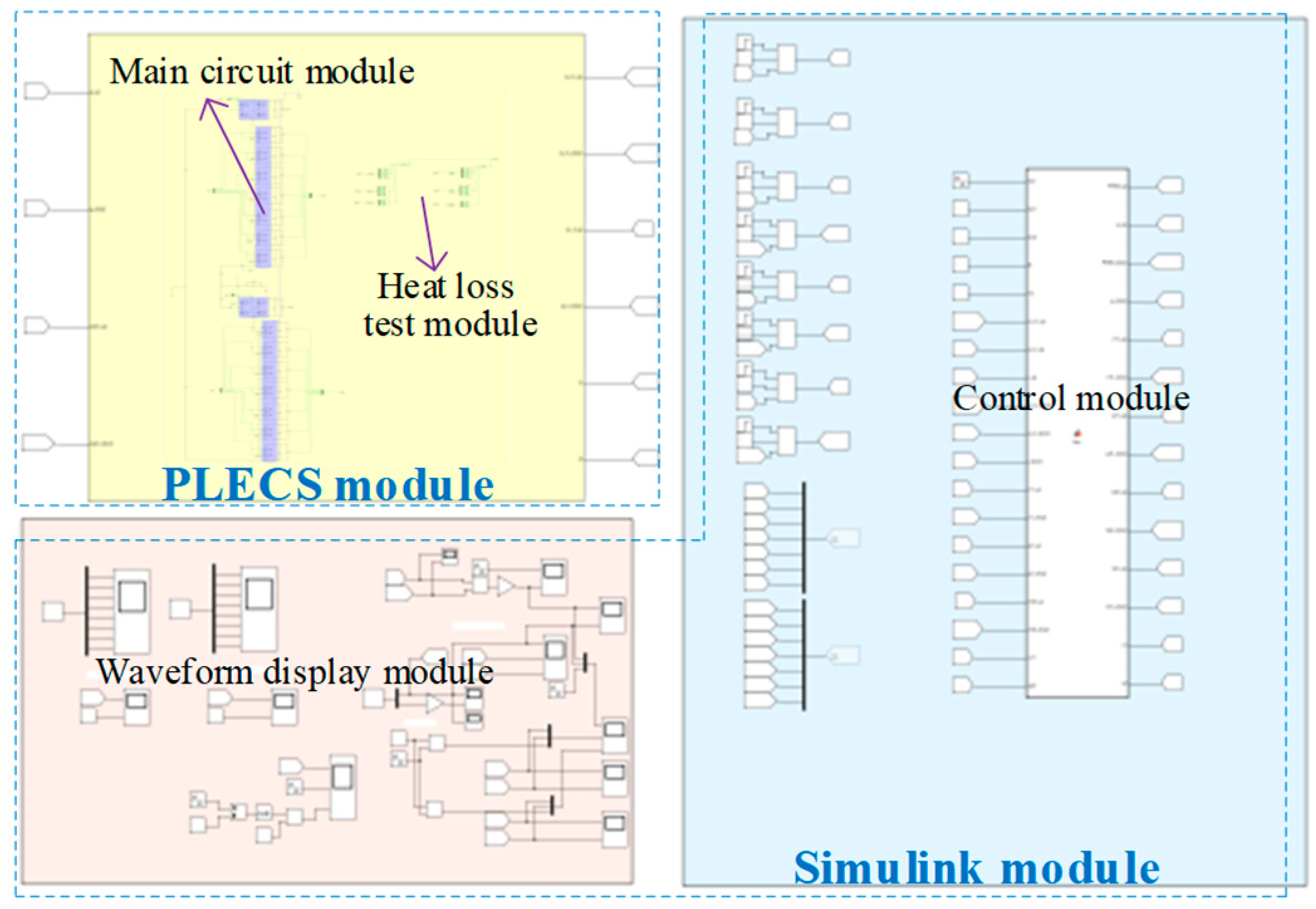
6. Experimental Analysis

To further substantiate the practicality of the introduced topology alongside its modulation method and voltage balancing approach, a single-phase HMMC low-voltage experimental platform is built. The experimental parameters are shown in Table 2.
The output voltage of the upper bridge arm uao_p, the output voltage of the low-frequency module ustep_p, the output voltage of the HCCM upwm_p, and the output voltage of the LFSM ustep_p1 of the HMMC are shown in Figure 9. The total number of levels is 17, and the switching time of the two modulation modes is shown in the diagram. The output voltage of the HCCM is a five-level high-frequency PWM wave, and the output voltage of the LFSM is a two-level low-frequency square wave.
The experimental waveform of the capacitor voltage of the NMMC sub-module is shown in Figure 10, which gives the capacitor voltages of two LFSMs and two capacitor voltages in the HCCM. The capacitor voltage of LFSM can be stabilized to about 75 V, while the HCCM capacitor voltage is stabilized to about 37.5 V, which conclusively demonstrates the efficacy of the presented voltage stabilization approach.
Furthermore, to authenticate the performance of the introduced topology and modulation methodology under transient conditions, the experimental waveforms under variable modulation coefficient and variable load conditions are given, respectively, as shown in Figure 10. The waveform of variable modulation coefficient is shown in Figure 11a. In 0–0.1 s, the modulation coefficient m = 0.9; in 0.1–0.2 s, the modulation coefficient m = 0.7; the output waveform is still consistent with the theoretical analysis and the DC-side capacitor voltage is stable. The waveform of the variable load condition is shown in Figure 11b. In 0–0.1 s, the output current amplitude Im = 23 A, and in 0.1–0.2 s, the output current amplitude Im = 11.5 A; the output waveform is still consistent with the theoretical analysis and the DC-side capacitor voltage is stable. Therefore, the effectiveness of the proposed topology and modulation strategy under transient conditions is effectively verified.

7. Comparison of Device Cost and Loss

7.1. Device Cost Comparison

The device cost is the main component of the total cost of the device. To further verify the advantages of the proposed topology, the device cost of the proposed topology is compared with the existing topology. The device cost comparison of the MMC based on an all-Si IGBT device (Si MMC), the MMC based on an all-SiC MOSFET device (SiC MMC), the topology proposed in [22], and the proposed NMMC topology is shown in Table 3. Among them, the Si IGBT selects 1700 V/300 A devices, and the SiC MOSFET devices select 1700 V/300 A and 1200 V/300 A devices, respectively. The market price ranges for the modules with similar specifications and different distributors are given. The device cost range of the all-Si MMC is USD 5558.4–11,692.8; The device cost range of the all-SiC MMC is USD 48,307.2–64,243.2; The device cost range of the topology proposed in [22] is USD 23,410.8–31,164. The device cost range of the proposed NMMC ranges from USD 14,832 to USD 22,159.2. Therefore, the device price of the proposed NMMC is significantly lower than that of the all-SiC MMC and the topology proposed in [22].

7.2. Loss Comparison

To prove the advantages of the proposed scheme in terms of operating loss, based on the joint simulation platform of MATLAB/Simulink 2016 version and PLECS-Blockset 9.2 version, the heat loss models of the Si MMC topology, SiC MMC topology, topology proposed in [22], and NMMC topology proposed in this study are built under the condition of a similar waveform quality. Among them, the topological parameters are consistent with Table 2. The simulation model is shown in Figure 12. The simulated main circuit and heat loss test module are located in PLCES, and the simulated control circuit and waveform test module are located in Simulink.
Under the condition of device junction temperature Tj = 100 °C and equivalent output switching frequency feq = 20 kHz, the loss comparison of the four topologies at different load power is shown in Figure 13. In terms of on-state loss, as the load power increases, the on-state loss in the four topologies increases. Among them, the on-state loss in the SiC-MMC topology increases fastest with the increase in power. In terms of switching loss, the switching loss in the Si-MMC topology is much higher than that of other topologies, while the switching loss in the SiC-MMC topology is the smallest. For the total loss, the loss in the Si-MMC topology is the largest and the loss in the SiC-MMC topology is the smallest under low-power conditions. Under high-power conditions, due to the sharp increase in the on-state loss in the SiC-MMC topology, the total loss is even higher than the total loss in the proposed NMMC topology. Taking the load power of 2.1 MW as an example, the total loss in the proposed NMMC topology is 29.7%, 6.7%, and 10.4% lower than that in the Si-MMC topology, SiC-MMC topology, and the topology proposed in [22], respectively.
Under the condition of the device junction temperature Tj = 100 °C and load power P = 1.5 MW, the loss comparison of the four topologies at different equivalent output switching frequencies is shown in Figure 14. Since the on-state loss is not affected by the change in switching frequency, the on-state loss remains basically unchanged. In terms of switching loss, the switching loss in the Si-MMC topology is the largest and increases fastest with the increase in switching frequency, while the switching loss in the SiC-MMC topology is the smallest. For the total loss, the loss in the proposed NMMC topology is much lower than that of the Si-MMC topology and the topology proposed in [22], and is close to that of the SiC-MMC topology. Taking the rated load power of 1.5 MW as an example, the total loss in the proposed NMMC topology is 37.5% and 23.4% lower than that of the Si-MMC topology and the topology proposed in [22], respectively.

8. Conclusions

To solve the problem of the difficultly in effectively balancing the output performance improvement, cost reduction, and efficiency improvement of traditional medium-voltage modular multilevel converters, this study proposes a new modular multilevel converter (NMMC) topology and its specific modulation and control strategy from the perspectives of modulation optimization and heterogeneous device mixing. The conclusions drawn are as follows:
(1)
The proposed NMMC topology can output 2N + 1 levels with only one high-frequency sub-module for each leg. The number of SiC MOSFET devices is lower, and the total cost of the devices is lower.
(2)
Under the premise of ensuring the quality of the output waveform, the hybrid modulation strategy is used to focus the high-frequency action on the SiC MOSFET devices and the low-frequency action on the Si IGBT devices. Under the condition of a high equivalent switching frequency and a high output power, the operation efficiency of the proposed scheme is more obvious than that of the existing scheme.
(3)
A thorough examination of the energy fluctuation dynamics within the high-frequency submodule DC capacitor is conducted, leading to the formulation of a tailored voltage balancing strategy. This strategy proficiently ensures the stability of both high- and low-frequency submodule capacitor voltages.

Author Contributions

Conceptualization, Q.G. and C.T.; investigation, H.B., M.X., R.Y., and Y.L.; writing—review and editing, Z.H. and Y.H. All authors have read and agreed to the published version of the manuscript.

Funding

This work is supported by the Science and Technology Project of China Southern Power Grid Corporation (090000KC23020073). The funder was not involved in the study design, collection, analysis, interpretation of data, the writing of this article, or the decision to submit it for publication.

Data Availability Statement

No new data were created or analyzed in this study. Data sharing is not applicable to this article.

Conflicts of Interest

The authors Hao Bai, Min Xu, Ruotian Yao and Yipeng Liu by the company China Southern Power Grid (SGCC). The remaining authors declare that the research was conducted in the absence of any commercial or financial relationships that could be construed as a potential conflict of interest.

Abbreviations

ParametersDefinitions
UdcDC-side voltage of the NMMC
UcDC-side capacitor voltage of low-frequency submodule
UcDC-side capacitor voltage of high-frequency submodule
UaoOutput voltage of the phase a of the NMMC
UmOutput voltage amplitude
ωThe angular frequency
mThe modulation factor
uao_prModulation wave of the upper arm of phase a
nstep_paThe number of sub-modules that need to be put into the low-frequency sub-module of the bridge arm on phase a
floor(x)A down-integer function
upwm_parReference value of the output voltage of the high-frequency sub-module of the bridge arm on phase a
ustep_paStep-wave voltage of the low-frequency sub-module in mode II
nstep_paThe number of sub-modules that need to be invested in the low-frequency sub-module of the bridge arm on phase a
upwm_parOutput voltage reference value of the high-frequency sub-module of the bridge arm on phase a
SpaAverage switching function of the high-frequency sub-module of the bridge arm on phase a
iarm_paThe bridge arm current on phase a
Δ E C _ pa The total energy fluctuation of the DC-side capacitor of the high-frequency sub-module of the upper arm of a
SpaThe average switching function of the high-frequency bridge arm of the upper arm of phase a
Δ E C _ pa The total energy fluctuation of the DC-side capacitor of the high-frequency sub-module in mode II

References

  1. Belhaouane, M.M.; Ayari, M.; Guillaud, X.; Braiek, N.B. Robust Control Design of MMC-HVDC Systems Using Multivariable Optimal Guaranteed Cost Approach. IEEE Trans. Ind. Appl. 2019, 55, 2952–2963. [Google Scholar] [CrossRef]
  2. Hao, Q.; Li, Z.; Gao, F.; Zhang, J. Reduced-Order Small-Signal Models of Modular Multilevel Converter and MMC-Based HVdc Grid. IEEE Trans. Ind. Electron. 2018, 66, 2257–2268. [Google Scholar] [CrossRef]
  3. Hou, Y.; Guo, Q.; Ren, P.; Tu, C.; Huang, Z.; Jia, W. A Hybrid Cascaded Multilevel Converter Based on Si and SiC Devices and Its Regulation Optimization Strategy. IEEE Trans. Ind. Appl. 2024, 60, 4001–4011. [Google Scholar] [CrossRef]
  4. Karwatzki, D.; Mertens, A. Generalized Control Approach for a Class of Modular Multilevel Converter Topologies. IEEE Trans. Power Electron. 2017, 33, 2888–2900. [Google Scholar] [CrossRef]
  5. Guo, Q.; Hou, Y.; Tu, C.; Zhou, Z.; Zhang, H.; Yu, L.; Wang, L.; Jiang, F.; Wang, X. A Novel Hybrid Modular Multilevel Converter with Three-Phase Coupled High-Frequency Modules for Multi-Index Optimization. IEEE Trans. Transp. Electrif. 2024; early access. [Google Scholar] [CrossRef]
  6. Zhao, P.; Meng, Y.; Ge, M.; Duan, Z.; Wang, X.; Wang, J. Series-Parallel Multiple Integrated Modular Multilevel DC-DC Converter for All-DC Offshore Wind Power System. IEEE Trans. Power Deliv. 2024, 39, 2482–2494. [Google Scholar] [CrossRef]
  7. Tang, C.; Thiringer, T. A Model Predictive Control Method with Adaptive Weighting Factors for Enhancing Performance of Modular Multilevel Converters. IEEE J. Emerg. Sel. Top. Power Electron. 2024, 12, 3887–3899. [Google Scholar] [CrossRef]
  8. Geng, Z.; Yang, Y.; Xiao, Y.; Xie, W. A Submodule Fault-Tolerant Operation Scheme of Modular Multilevel Converters Through Novel Cold and Hot Mixed Topology. IEEE Trans. Power Deliv. 2024, 39, 2470–2481. [Google Scholar] [CrossRef]
  9. Pratheesh, K.J.; Jagadanand, G.; Ramchand, R. A Generalized-Switch-Matrix-Based Space Vector Modulation Technique Using the Nearest Level Modulation Concept for Neutral-Point-Clamped Multilevel Inverters. IEEE Trans. Ind. Electron. 2018, 65, 4542–4552. [Google Scholar] [CrossRef]
  10. Miyama, Y.; Ishizuka, M.; Kometani, H.; Akatsu, K. Vibration Reduction by Applying Carrier Phase-Shift PWM on Dual Three-Phase Winding Permanent Magnet Synchronous Motor. IEEE Trans. Ind. Appl. 2018, 54, 5998–6004. [Google Scholar] [CrossRef]
  11. Ronanki, D.; Williamson, S.S. A Novel 2 N + 1 Carrier-Based Pulse Width Modulation Scheme for Modular Multilevel Converters with Reduced Control Complexity. IEEE Trans. Ind. Appl. 2020, 56, 5593–5602. [Google Scholar] [CrossRef]
  12. Hu, P.; Jiang, D. A Level-Increased Nearest Level Modulation Method for Modular Multilevel Converters. IEEE Trans. Power Electron. 2014, 30, 1836–1842. [Google Scholar] [CrossRef]
  13. Wu, D.; Peng, L. Characteristics of nearest level modulation method with circulating current control for modular multilevel converter. IET Power Electron. 2016, 9, 155–164. [Google Scholar] [CrossRef]
  14. Wang, Y.; Hu, C.; Ding, R.; Xu, L.; Fu, C.; Yang, E. A Nearest Level PWM Method for the MMC in DC Distribution Grids. IEEE Trans. Power Electron. 2018, 33, 9209–9218. [Google Scholar] [CrossRef]
  15. Wang, Z.; Peng, L.; Zhang, J. Decomposed Nearest Level PWM Method With Reduced Switching Frequency for MMC. IEEE Trans. Power Electron. 2022, 38, 3340–3351. [Google Scholar] [CrossRef]
  16. Yang, G.; Zhou, S.; Peng, G.; Wu, W.; Xin, Q.; Xu, S. An improved hybrid modulation control strategy for MMC with auxiliary sub-modules. J. Power Supply 2024, 22, 74–82. [Google Scholar]
  17. Miu, H.; Mei, J.; Zhang, C.; Zheng, J.; Mei, F. A novel topology of n+1 hybrid modular multilevel converter and its control strategy. Electr. Power Autom. Equip. 2018, 38, 88–95. [Google Scholar]
  18. Shahane, R.; Belkhode, S.; Shukla, A.; Doolla, S. A Highly Efficient Hybrid Devices-based MMC with a Novel Modulation Scheme Using Hardware-in- Loop System. In Proceedings of the 2022 IEEE Applied Power Electronics Conference and Exposition (APEC), Houston, TX, USA, 20–24 March 2022; pp. 675–680. [Google Scholar]
  19. Li, C.; Lu, R.; Li, C.; Li, W.; Gu, X.; Fang, Y.; Ma, H.; He, X. Space Vector Modulation for SiC and Si Hybrid ANPC Converter in Medium-Voltage High-Speed Drive System. IEEE Trans. Power Electron. 2019, 35, 3390–3401. [Google Scholar] [CrossRef]
  20. Liu, C.; Zhuang, K.; Pei, Z.; Zhu, D.; Li, X.; Yu, Q.; Xin, H. Hybrid SiC-Si DC–AC Topology: SHEPWM Si-IGBT Master Unit Handling High Power Integrated with Partial-Power SiC-MOSFET Slave Unit Improving Performance. IEEE Trans. Power Electron. 2022, 37, 3085–3098. [Google Scholar] [CrossRef]
  21. Zhang, C.; Wang, J.; Qu, K.; Hu, B.; Li, Z.; Yin, X.; Shen, Z. WBG and Si Hybrid Half-Bridge Power Processing Toward Optimal Efficiency, Power Quality, and Cost Tradeoff. IEEE Trans. Power Electron. 2022, 37, 6844–6856. [Google Scholar] [CrossRef]
  22. Yin, T.; Lin, L.; Xu, C.; Zhu, D.; Jing, K. A Hybrid Modular Multilevel Converter Comprising SiC MOSFET and Si IGBT with Its Specialized Modulation and Voltage Balancing Scheme. IEEE Trans. Ind. Electron. 2022, 69, 11272–11282. [Google Scholar] [CrossRef]
  23. Kiehnle, P.; Himmelmann, P.; Hiller, M. GaN-Based Modular Multilevel Converter for Low-Voltage Grid Enables High Efficiency. In Proceedings of the 2022 24th European Conference on Power Electronics and Applications (EPE’22 ECCE Europe), Hanover, Germany, 5–9 September 2022; pp. 1–7. [Google Scholar]
  24. Kiehnle, P.; Katzenburg, N.; Stefanski, L.; Hiller, M. Hybrid Implementation of Cascade Control for GaN-Based Modular Multilevel Converter for Low-Voltage Grid. In Proceedings of the 2023 25th European Conference on Power Electronics and Applications (EPE’23 ECCE Europe), Aalborg, Denmark, 4–8 September 2023; pp. 1–10. [Google Scholar]
  25. Avila, A.; Garcia-Bediaga, A.; Oñederra, O.; Ruias, A.; Rodriguez, A. Comparative analysis of GaN HEMT vs. Si CoolMOS for a high-frequency MMC topology. In Proceedings of the 2017 19th European Conference on Power Electronics and Applications (EPE’17 ECCE Europe), Warsaw, Poland, 11–14 September 2017; pp. 1–9. [Google Scholar]
Figure 1. Topology diagram of the NMMC.
Electronics 13 03656 g001
Figure 2. Modulation principle of the NMMC.
Electronics 13 03656 g002
Figure 3. PWM principle of the HCCM.
Electronics 13 03656 g003
Figure 4. Total energy change diagram of HCCM in mode I.
Electronics 13 03656 g004
Figure 5. Total energy change diagram of HCCM in mode II.
Electronics 13 03656 g005
Figure 6. Working state of the HCCM in mode I. (a) S2, T1 and T4 are switched on. (b) S2, T2 and T4 are switched on. (c) S2, T1 and T3 are switched on. (d) S2, T2 and T3 are switched on. (e) S2, T1 and T4 are switched on. (f) S2, T2 and T4 are switched on. (g) S2, T1 and T3 are switched on. (h) S2, T2 and T3 are switched on.
Electronics 13 03656 g006
Figure 7. Working state of the HCCM in mode II. (a) S1, T2 and T3 are turned on. (b) S1, T1 and T3 are turned on. (c) S1, T2 and T4 are turned on. (d) S1, T1 and T4 are turned on. (e) S1, T2 and T3 are turned on. (f) S1, T1 and T3 are turned on. (g) S1, T2 and T4 are turned on. (h) S1, T1 and T4 are turned on.
Electronics 13 03656 g007
Figure 8. Voltage balancing process of the HCCM.
Electronics 13 03656 g008
Figure 9. The output waveform.
Electronics 13 03656 g009
Figure 10. Capacitance voltage waveform.
Electronics 13 03656 g010
Figure 11. Experimental waveforms of HMMC under transient conditions.
Electronics 13 03656 g011
Figure 12. Joint simulation model of MATLAB/Simulink and PLECS.
Electronics 13 03656 g012
Figure 13. Loss comparison under different load power (Tj = 100 °C, feq = 20 kHz).
Electronics 13 03656 g013
Figure 14. Loss comparison at different equivalent switching frequencies (Tj = 100 °C, P = 1.5 MW).
Electronics 13 03656 g014
Table 1. Switching mode of the HCCM.
S1S2T1T2T3T4Output Voltage
011001Uc
010101Uc/2
011010Uc/2
0101100
100110Uc
101010Uc/2
100101Uc/2
1010010
Table 2. Experiment parameters.
ParameterValue
Number of bridge arm sub-modules N8
DC-side voltage Udc of NMMC 600 V
DC-side capacitor voltage Uc of the sub-module 75 V
DC-side capacitance CL of LFSM 3.8 mF
DC-side capacitance CH of the HCCM3.8 mF
Bridge arm inductance L3 mH
Carrier frequency fc10 kHz
Modulation coefficient m0.9
Table 3. Device cost comparison.
DeviceSi-MMCSiC-MMCRef. [22]Proposed NMMC
Si IGBT (1700 V/300 A)
Model/Price
FF300R17ME4: USD 69.196/8496
FF300R17KE3:
USD 94.5–121.8
FF300R17ME4_B11: USD 71.43–77.51
FF300R17ME4P_B11: USD 71.2–83.13
FF300R17KE4P:
USD 73.15
FF300R17ME7_B11: USD 67.88–77.32
FF300R17KE4:
USD 57.9–86
IFF300B17N2E4P_B11: USD 105.6–118.6
FF300R17ME4P:
USD 75.2–83.13
SiC MOSFET (1700 V/300 A)
Model/Price
CAB320M17XM3: USD 603.9–669.2/96//
WAS310M17BM3: USD 553.9–611.2
CAS310M17BM3:
USD 503.2–555.4
SiC MOSFET (1200 V/300 A)
Model/Price
CAS300M12BM2:
USD 386.4–430.2
//4824
WAB300M12BM3: USD 394.6–436.1
Cost USD 5558.4–11,692.8USD 48307.2–64,243.2USD 23,410.8–31,164USD 14,832–22,159.2
Disclaimer/Publisher’s Note: The statements, opinions and data contained in all publications are solely those of the individual author(s) and contributor(s) and not of MDPI and/or the editor(s). MDPI and/or the editor(s) disclaim responsibility for any injury to people or property resulting from any ideas, methods, instructions or products referred to in the content.

