Communication

Analysis of Influencing Factors on Multilevel Storage Performance in Phase-Change Random Access Memory

by
Zhiyu Wang
1,* and
Daolin Cai
2,*
1
School of Integrated Circuits, Jiangnan University, Wuxi 214122, China
2
School of Integrated Circuits, East China Normal University, Shanghai 200241, China
*
Authors to whom correspondence should be addressed.
Electronics 2024, 13(19), 3802; https://doi.org/10.3390/electronics13193802
Submission received: 8 September 2024 / Revised: 24 September 2024 / Accepted: 24 September 2024 / Published: 25 September 2024
(This article belongs to the Special Issue Advanced CMOS Devices and Applications, 2nd Edition)

Abstract

:
In response to the growing demand for advanced memory technologies, this study investigates a 4 Mb phase-change memory (PCRAM) chip employing a carbon-doped Ge2Sb2Te5 (C-GST) dielectric material to achieve multistage storage. The Partial-RESET programming and verification (P&V) method was utilized to effectively create intermediate-resistance states, facilitating multilevel storage. The study focuses on optimizing the key parameters affecting the P&V method to enhance the precision and efficiency of reaching intermediate resistance values. Through comprehensive experimentation on the PCRAM array, this work evaluates the performance of multilevel storage, providing insights into the potential for scalable, high-density memory applications.

1. Introduction

Phase-change random access memory (PCRAM) is a type of semiconductor memory that utilizes sulfur compounds, with Ge2Sb2Te5 (GST) being the most representative material. PCRAM operates by employing current pulses to generate Joule heat, which facilitates a phase transition between crystalline (SET state, characterized by lower resistivity) and amorphous (RESET state, characterized by higher resistivity) structures. This differential in resistance values is leveraged to encode binary data as “0” and “1”. PCRAM is technically compatible with standard complementary metal-oxide-semiconductor (CMOS) technology [1]. The technology offers several advantages, including high-speed operation, excellent fatigue resistance, and the capability for miniaturization at process nodes of 22 nm and below [2,3,4,5]. Additionally, the significant resistance disparity between the high- and low-resistance states in PCRAM suggests the potential for multilevel storage [6]. PCRAM is widely used in storage class memory (SCM), solid-state drives, and neuromorphic chips [7,8]. And the on–off characteristics of phase-change material can be used in electro-optical switches like monolithically integrated silicon light-emitting devices (LEDs) [9].
In 1995, Ovshinsky et al. [10] proposed the potential for manipulating PCRAM cells to achieve intermediate-resistance states. In recent years, the rapid development of internet of things (IoT), cloud services, big data, and artificial intelligence applications has significantly increased the demand for high memory density [11]. To enhance storage capacity, innovative manufacturing techniques such as 3D stacking and multilevel cell (MLC) design have been employed, allowing for the storage of multiple bits within a single cell [12,13]. While multistage storage offers capacity advantages over single-stage cell technology, it is accompanied by drawbacks such as reduced battery life, as well as challenges including resistance drift and read interference, which can compromise the reliability of multistage devices [14]. In this work, MLC storage was implemented in a 4 Mb PCRAM chip based on the 40 nm node. The multilevel storage mechanism of CGST PCRAM is studied in reference [15], but the operating parameters affecting the multilevel storage of PCRAM are not studied systematically. In this paper, the operating parameters pulse width (TRST), pulse current increase (ΔI), and starting current (IStart) are studied. The parameters lay a foundation for the commercialization of PCRAM. This paper utilizes the Partial-RESET programming and verification (P&V) method to facilitate multilevel storage in PCRAM based on carbon-doped Ge2Sb2Te5 (C-GST) dielectric material, with a particular focus on examining the factors that affect the Partial-RESET programming approach. This research aims to provide a foundational reference for optimizing the implementation of multilevel storage in the future, thereby contributing to the high-density application and commercialization of PCRAM.

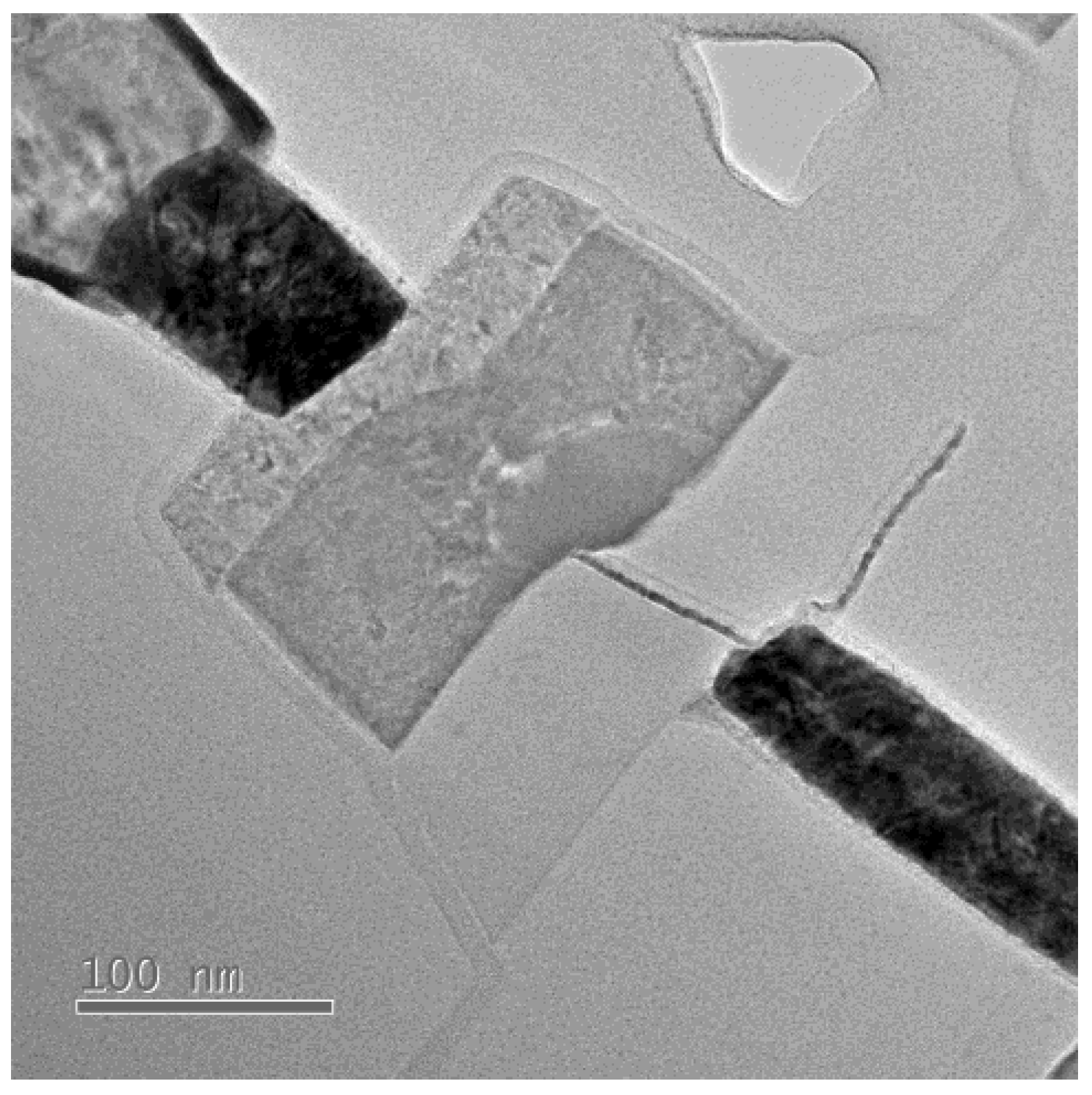
2. Experimental Devices and Experimental Methods

The sample analyzed was a 4 Mb capacity PCRAM chip produced by SMIC, utilizing a 40 nm fabrication process. Figure 1 shows the cross-section of a memory cell integrated based on the 40 nm node. The PCRAM unit is built between CT and Metal 1 by adding only three extra masks. The blade bottom electrode contact (BEC) acted as the heating electrode, which was designed as a titanium nitride (TiN) blade type, characterized by a height of 100 nm and a thickness of 6 nm, with one side protected by a silicon nitride (SiN) layer. And the typical metal-oxide semiconductor field effect transistor (MOSFET) acted as the selector. A lance-shaped CGST film was placed above the BEC. The top and the bottom electrode were made of metal tungsten (W) and the TiN film acted as an adhesive layer.
In the Partial-RESET programming verification method, the initial Over-SET pulse is maintained as a fixed parameter, with the subsequent RESET pulse parameters being the primary focus of regulation and investigation. Three parameters were identified for regulation: pulse width (TRST), pulse current increase (ΔI), and starting current (IStart).

3. Results and Discussion

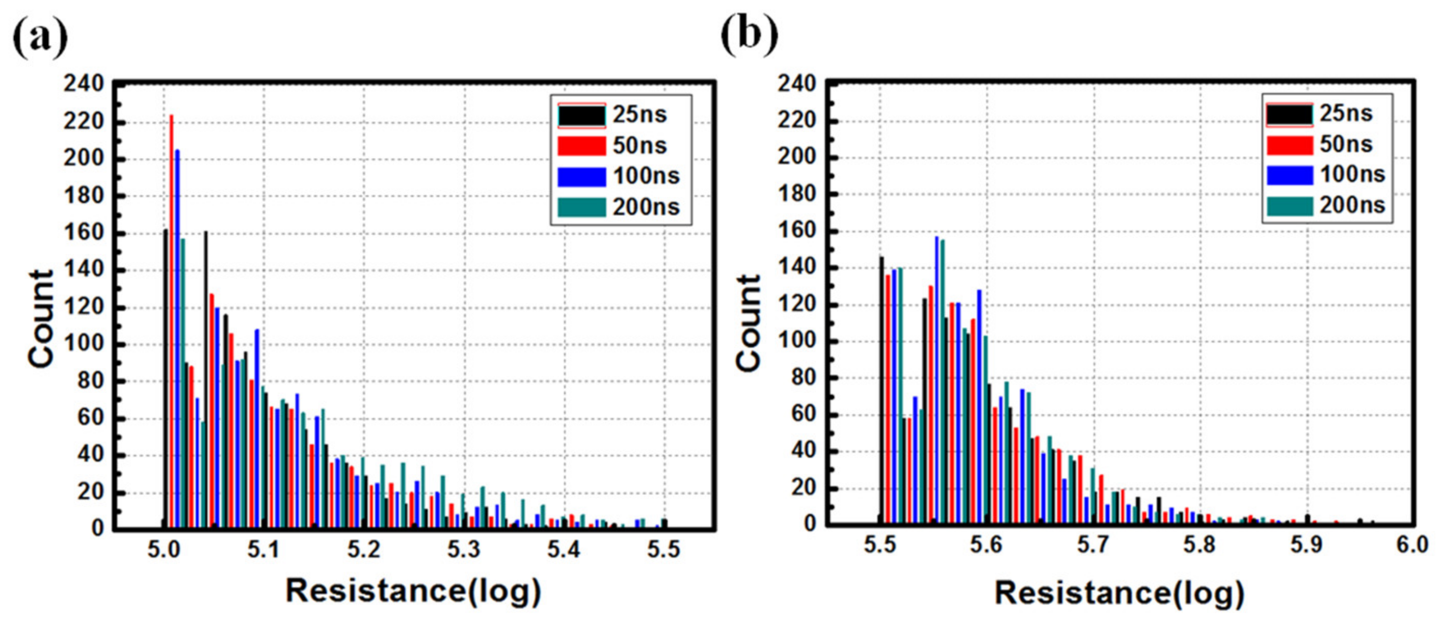
3.1. Effect of TRST on Multilevel Storage

In the investigation of the effect of TRST on the programming verification method, the IStart of the series RESET pulse was maintained at 0.2 mA, while the ΔI was set to 10 μA. TRST values were varied at 25 ns, 50 ns, 100 ns, and 200 ns. The resulting programming verification resistance–current (R-I) curve, which illustrates the variation in resistance with respect to the RESET current, is depicted in Figure 2. Notably, despite the different TRST values employed, the overall shape of the curve remained consistent. The resistance values recorded at equivalent currents exhibited only minor fluctuations, and both the slope of the curve and the rate of resistance change were nearly identical. These results suggest that the width of the RESET pulse has a minimal effect on the characteristics of the curve within the programming verification method.
The resistance distribution of a 1 Kb PCRAM cell was evaluated by analyzing the resistance of the intermediate state (IStop) across various TRST values, as previously described. The resistance distribution histogram for the ‘10’ state, which had a resistance value from 105 to 105.5 Ω, is presented in Figure 3a, while the histogram for the ‘01’ state, which had a resistance value from 105.5 to 106, is depicted in Figure 3b. In comparison to the resistance histogram of the ‘10’ state, there is a noticeable decrease in the number of units approaching the lower limit of the resistance range for the ‘01’ state. Furthermore, the trend of a decreasing number of units exhibits a more linear pattern as the resistance value increases.

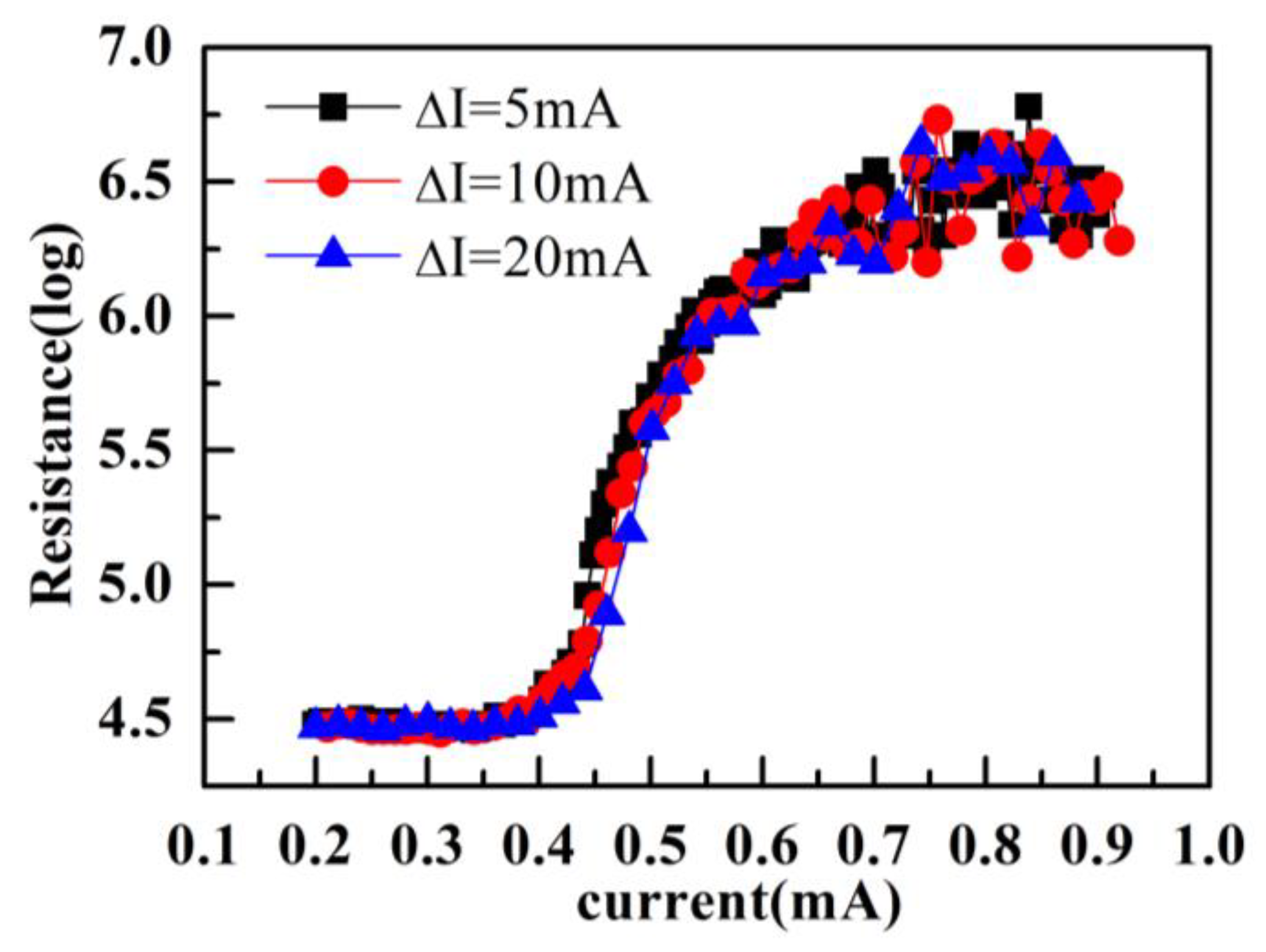
3.2. Effect of Pulse Increase on Multilevel Storage

ΔI refers to the increase in pulse height of a subsequent RESET pulse in comparison to that of the preceding RESET pulse. In this experiment, RESET ΔI values were established at 5 μA, 10 μA, and 20 μA. The programming under these varying ΔI values was conducted to assess the alterations in the R-I curve. The measured resistance curve corresponding to the current variations is illustrated in Figure 4. As the RESET ΔI increased, the resistance exhibited a more rapid increase. Specifically, the resistance changed most slowly when the ΔI was set at 5 μA, while it changed most rapidly at 20 μA. As the current increased, the resistance increased slowly, so the graph also changes from vertical to gentle. However, R-I curves for the three increments remained consistent. A smaller ΔI resulted in a slower change in resistance, which may have facilitated a more precise attainment of the target resistance value. Conversely, a larger ΔI necessitated a greater number of pulses to achieve the same resistance value, thereby prolonging the time required to reach the IStop.
The current necessary to achieve the IStop was calculated using a programming algorithm that employed different ΔI values on a PCRAM unit with an array size of 1 Kb. The results of the current distribution histogram are presented in Figure 5. In the three tests conducted with different ΔI values, the current distribution required to attain the ‘01’ state was observed to be positioned to the right of the current distribution necessary to reach the ‘10’ state. This observation indicates that the current required to achieve the ‘01’ state was greater than that required for the ‘10’ state. Consequently, this implies that a higher number of pulses and a longer duration were necessary, as the resistance associated with the ‘01’ state was greater than that of the ‘10’ state. Furthermore, due to the inherent differences among storage units, the current required to reach the same state exhibited variability, resulting in an overlap of the current distributions necessary to attain the two IStop values. Despite the variations in ΔI, the current required to reach the ‘10’ state predominantly fell within the range of 0.41~0.51 mA, while the current required to achieve the ‘01’ state was primarily concentrated in the range of 0.48–0.56 mA. Notably, alterations in ΔI did not significantly affect the current required to reach the IStop.
Two IStop values of resistance distribution were obtained through programming verification methods utilizing ΔI values of 5 μA, 10 μA, and 20 μA (Figure 6). The analysis of the test results indicates that smaller ΔI values yield a high success rate in achieving the IStop of multistage storage, resulting in a more concentrated resistance distribution, which enhances the reliability of multistage storage. However, smaller ΔI values also lead to slower resistance changes. While the accuracy of achieving the IStop improves, this comes at the cost of increased time required to reach that state. Therefore, it is essential to ensure a high success rate for the IStop while employing appropriate ΔI values whenever feasible.

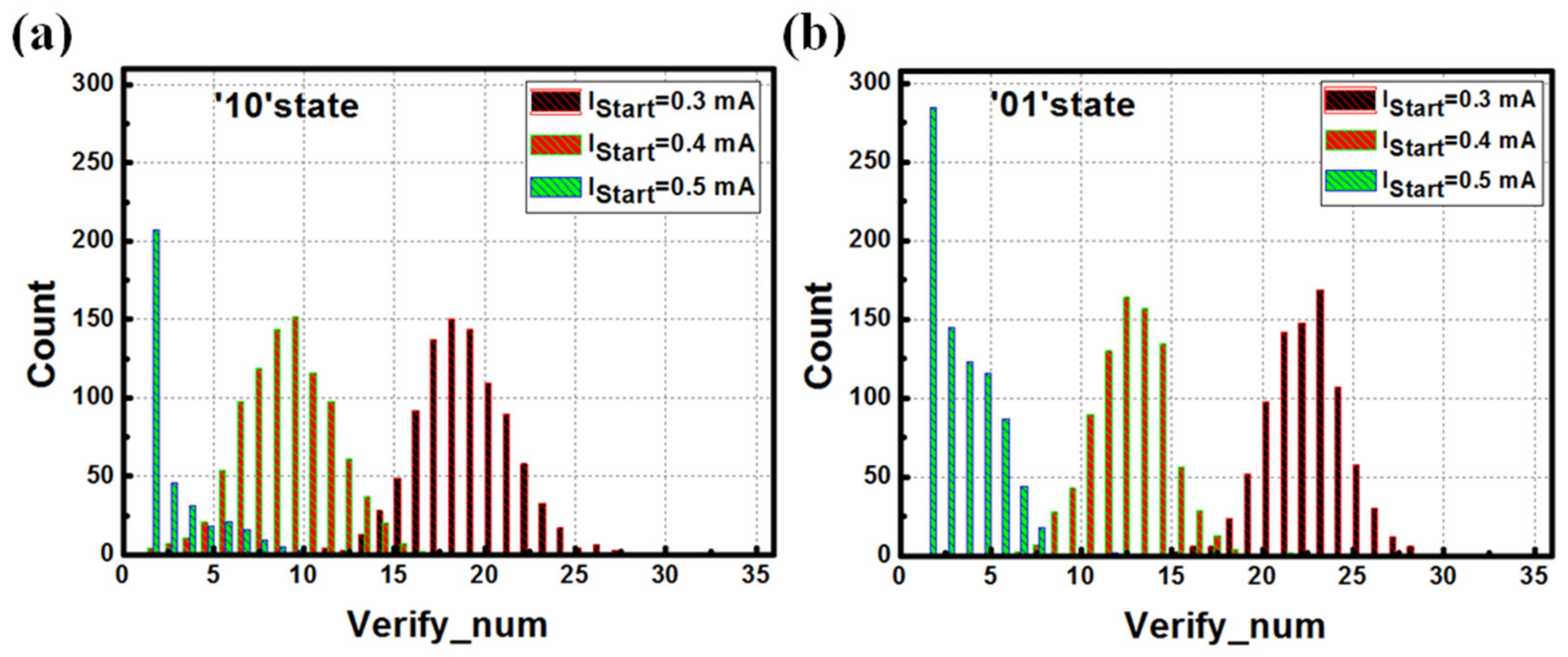
3.3. Effect of IStart on Multilevel Storage

The effect of employing the Partial-RESET programming verification method with varying IStart (R-I curve) values, which depicts the change in resistance relative to current during the programming verification process, is presented in Figure 7. In the series of RESET pulses, IStart values were established at 0.2 mA, 0.3 mA, 0.4 mA, 0.5 mA, and 0.6 mA. The increments of ΔI and TRST were maintained at 10 μA and 50 ns, respectively. The resistance remained unchanged until the IStart reached 0.3 mA, indicating that an IStart of 0.3 mA was functionally equivalent to that of 0.2 mA. During the transition of the storage unit from the crystalline state to the amorphous state, variations in IStart resulted in corresponding differences in the initial resistance values; specifically, higher IStart values correlated with elevated initial resistance values within the programming algorithm. However, the overall shape of the programming curve remained consistent across different IStart values, and only a minimal portion of the RESET pulse was necessary to mitigate the dependence of the programming curve on the IStart. This result contributes to enhanced programming speed and a reduction in the number of pulses required to achieve the IStop.
In the programming verification method, after establishing the IStart and ΔI, the number of programming pulses (n) necessary to achieve IStop can be calculated using Equation (1):
n = I S t o p I S t a r t / I
Based on the test results, the current necessary to attain the IStop was distributed within a fixed range of current values. Consequently, programming time could be reduced by adjusting the IStart in accordance with the target resistances of various IStop values. The distribution of pulses required to achieve the ‘10’ and ‘01’ states, following tests with different IStart values on a 1 Kb storage unit array, is illustrated in Figure 8. As the IStart increased, the number of pulses required for both IStop values decreased. Specifically, when the IStart was set at 0.5 mA, the number of pulses needed to reach the two IStop values was fewer than five, with the majority of storage units attaining the target resistance value within two to three RESET pulses. Therefore, selecting an appropriate IStart can effectively minimize the number of pulses required to reach the IStop, thereby reducing programming time.
To further investigate the effects of varying the IStart on the performance of multilevel storage, the resistance distributions obtained through the programming verification algorithm at an IStart of 0.3 mA, 0.4 mA, and 0.5 mA are presented in Figure 9. The resistance distributions for the ‘10’ IStop under the conditions of 0.3 mA and 0.4 mA were nearly identical. However, the resistance distribution at 0.5 mA remained within the target resistance range but exhibited a slight rightward shift. This shift may be attributed to the relatively high IStart, which likely resulted in an elevated initial resistance, thereby displacing the overall target resistance value to a higher range. In the case of the ‘01’ IStop, no significant differences were observed in the resistance distributions across the three IStart values. Only a slight rightward movement in the resistance distribution was noted with the increase in IStart, which had a minimal effect on the performance and reliability of the IStop. While a larger IStart can effectively reduce programming time, an excessively high IStart may lead to an elevated IStop resistance value, which could compromise the reliability of multilevel storage. Therefore, it is essential to select an appropriate IStart based on the specific IStop, balancing the need to shorten programming time with the goal of ensuring optimal performance in multilevel storage. The cumulative probability of about 99.5% is insufficient, as shown in Figure 8. Increasing the number of operable cell samples and improving resistance for the more precise control can enhance the cumulative probability.
Following a comprehensive analysis and optimization of the parameters associated with the RESET pulse, four-state multistage storage of resistance values was attained. The distribution of resistance across the four states, along with the necessary operating conditions, is illustrated in Figure 10. The implementation of Over-SET and Over-RESET pulse operations was employed to guarantee that the resistance values conformed to the specifications for the fully crystallized ‘11’ state and the amorphous ‘00’ state.

4. Conclusions

This study focused on the use of C-GST PCRAM chips fabricated on SMIC’s 40 nm standard CMOS technology platform, investigating the key factors affecting the Partial-RESET programming verification method. Specifically, the effects of RESET TRST, current pulse increase, and IStart on the programming performance were examined in detail. The results indicate that RESET TRST has a minimal effect on the programming curve, while increasing the pulse current expedites the attainment of intermediate-resistance states but at the cost of a reduced success rate. Additionally, higher IStart values correspond to elevated initial resistance values. By adjusting the pulse ΔI and IStart based on the target intermediate resistance, the number of pulses required to achieve the IStop was minimized, leading to a significant improvement in programming speed. This optimization enabled reliable four-state storage in PCRAM, offering promising avenues for high-density memory applications.

Author Contributions

Conceptualization, Z.W. and D.C.; methodology, D.C.; software, D.C.; validation, Z.W.; formal analysis, D.C.; investigation, D.C.; resources, D.C.; data curation, Z.W.; writing—original draft preparation, D.C.; writing—review and editing, D.C.; visualization, Z.W.; supervision, Z.W.; project administration, D.C.; funding acquisition, D.C. All authors have read and agreed to the published version of the manuscript.

Funding

This research was funded by the National Natural Science Foundation of China under Grant 62204086, the Shanghai Science and Technology Funding Project under Grant 22DZ2205100, and the Shanghai Pujiang Program under Grant 22PJD019.

Data Availability Statement

The data presented in this study are available in this article.

Conflicts of Interest

The authors declare no conflicts of interest.

References

  1. Oh, J.H.; Park, J.H.; Lim, Y.S.; Lim, H.S.; Oh, Y.T.; Kim, J.S.; Shin, J.M.; Song, Y.J.; Ryoo, K.C.; Lim, D.W.; et al. Full integration of highly manufacturable 512 Mb PRAM based on 90 nm technology. In Proceedings of the IEEE International Electron Devices Meeting (IEDM), San Francisco, CA, USA, 11–13 December 2006; pp. 2.6.1–2.6.4. [Google Scholar]
  2. Rao, F.; Ding, K.Y.; Zhou, Y.X.; Zheng, Y.H.; Xia, M.J.; Lv, S.L.; Song, Z.T.; Feng, S.L.; Ronneberger, I.; Mazzarello, R.; et al. Reducing the stochasticity of crystal nucleation to enable subnanosecond memory writing. Science 2017, 358, 1423–1427. [Google Scholar] [CrossRef] [PubMed]
  3. Wong, H.S.; Salahuddin, S. Memory leads the way to better computing. Nat. Nanotechnol. 2015, 10, 191–194. [Google Scholar] [CrossRef] [PubMed]
  4. Chen, Y.C.; Rettner, C.T.; Raoux, S.; Burr, G.W.; Chen, S.H.; Shelby, R.M.; Salinga, M.; Risk, W.P.; Happ, T.D.; McClelland, G.M.; et al. Ultra-thin phase-change bridge memory device using GeSb. In Proceedings of the IEEE International Electron Devices Meeting (IEDM), San Francisco, CA, USA, 11–13 December 2006; pp. 30.3.1–30.3.4. [Google Scholar]
  5. Im, D.H.; Lee, J.I.; Cho, S.L.; An, H.G.; Kim, D.H.; Kim, I.S.; Park, H.; Ahn, D.H.; Horii, H.; Park, S.O.; et al. A Unified 7.5 nm Dash-Type Confined Cell for High Performance PRAM Device. In Proceedings of the IEEE International Electron Devices Meeting, San Francisco, CA, USA, 15–17 December 2008; pp. 1–4. [Google Scholar]
  6. Raoux, S.; Burr, G.W.; Breitwisch, M.J.; Rettner, C.T.; Chen, Y.C.; Shelby, R.M.; Salinga, M.; Krebs, D.; Chen, S.H.; Lung, H.L.; et al. Phase-change random access memory: A scalable technology. IBM J. Res. Dev. 2008, 52, 465–479. [Google Scholar] [CrossRef]
  7. Qureshi, M.K.; Srinivasan, V.; Rivers, J.A. Scalable high performance main memory system using phase-change memory technology. ACM Sigarch Comput. Archit. News 2009, 37, 24–33. [Google Scholar] [CrossRef]
  8. Tuma, T.; Pantazi, A.; Le Gallo, M.; Sebastian, A.; Nanotechnol, E. Stochastic phase-change neurons. Nat. Nanotechnol. 2016, 11, 693–699. [Google Scholar] [CrossRef] [PubMed]
  9. Xu, K. Silicon electro-optic micro-modulator fabricated in standard CMOS technology as components for all silicon monolithic integrated optoelectronic systems. J. Micromech. Microeng. 2021, 31, 054001. [Google Scholar] [CrossRef]
  10. Klersy, P.K.; Strand, D.A.; Ovshinsky, S.R. Electrically Erasable, Directly Overwritable, Multibit Single Cell Memory Element and Arrays Fabricated Therefrom. Google Patents. U.S. Patent 5536947A, 16 July 1996. [Google Scholar]
  11. Ahmad, I.; Imdoukh, M.; Alfailakawi, M.G. Extending multi-level STT-MRAM cell lifetime by minimising two-step and hard state transitions in hot bits. IET Comput. Digit. Tech. 2017, 11, 214–220. [Google Scholar] [CrossRef]
  12. Burr, G.W.; Brightsky, M.J.; Sebastian, A.; Cheng, H.Y.; Wu, J.Y.; Kim, S.; Sosa, N.E.; Papandreou, N.; Lung, H.L.; Pozidis, H. Recent Progress in Phase-Change Memory Technology. IEEE J. Emerg. Sel. Top. Circuits Syst. 2016, 6, 146–162. [Google Scholar] [CrossRef]
  13. Liu, L.; Gu, H.; Wu, W.; Wang, Z.; Lai, T. Multi-level phase-change behaviors of Ge2Sb2Te5/Sb7Se3 bilayer films and a design rule of multi-level phase-change films. J. Alloys Compd. 2024, 990, 174424. [Google Scholar] [CrossRef]
  14. Zhang, M.; Zhang, L.; Jiang, L.; Liu, Z.; Chong, F.T. Balancing Performance and Lifetime of MLC PCM by Using a Region Retention Monitor. In Proceedings of the 2017 IEEE International Symposium on High Performance Computer Architecture (HPCA), Austin, TX, USA, 4–8 February 2017; pp. 385–396. [Google Scholar] [CrossRef]
  15. Song, Z.; Cai, D.; Cheng, Y.; Wang, L.; Lv, S.; Xin, T.; Feng, G. 12-state multi-level cell storage implemented in a 128 Mb phase change memory chip. Nanoscale 2021, 13, 10455–10461. [Google Scholar] [CrossRef] [PubMed]
Figure 1. Cross-sectional TEM image of a cell in the PCRAM chip.
Electronics 13 03802 g001
Figure 2. P&V curves of different TRST values.
Electronics 13 03802 g002
Figure 3. Resistance distribution for IStop with different TRST values: (a) ‘10’ state; (b) ‘01’ state.
Electronics 13 03802 g003
Figure 4. R-I curves under P&V method with different ΔI values: ΔI = 5 μA, ΔI = 10 μA and ΔI = 20 μA.
Electronics 13 03802 g004
Figure 5. Current distribution required to achieve IStop with different ΔI values: (a) ΔI = 5 μA; (b) ΔI = 10 μA; (c) ΔI = 20 μA.
Electronics 13 03802 g005
Figure 6. Resistance distribution of IStop with different ΔI values.
Electronics 13 03802 g006
Figure 7. P&V curves for different programming IStart values (ΔI = 10 μA, TRST = 50 ns).
Electronics 13 03802 g007
Figure 8. Pulse number distribution for different IStop values with different programming IStart values: (a) ‘10’ state; (b) ‘01’ state.
Electronics 13 03802 g008
Figure 9. Resistance distribution of IStop with different programming IStart values: (a) ‘10’ state; (b) ‘01’ state.
Electronics 13 03802 g009
Figure 10. Distribution of four resistance levels.
Electronics 13 03802 g010
Disclaimer/Publisher’s Note: The statements, opinions and data contained in all publications are solely those of the individual author(s) and contributor(s) and not of MDPI and/or the editor(s). MDPI and/or the editor(s) disclaim responsibility for any injury to people or property resulting from any ideas, methods, instructions or products referred to in the content.

