Article

Miniaturized Multiband Substrate-Integrated Waveguide Bandpass Filters with Multi-Layer Configuration and High In-Band Isolation

1
School of Microelectronics and The Tianjin Key Laboratory of Imaging and Sensing Microelectronic Technology, Tianjin University, Tianjin 300072, China
2
Engineering Product Development, Singapore University of Technology and Design, Singapore 487372, Singapore
*
Author to whom correspondence should be addressed.
Electronics 2024, 13(19), 3834; https://doi.org/10.3390/electronics13193834
Submission received: 28 July 2024 / Revised: 20 September 2024 / Accepted: 25 September 2024 / Published: 28 September 2024

Abstract

:
This article presents a multiband bandpass filter structure with an in-line topology based on substrate-integrated waveguide (SIW) technology. A multi-layer configuration is employed to achieve circuit miniaturization. By constructing the coupling matrix, the coupling relationships among all resonators are quantitatively characterized, enabling the extraction of the theoretical frequency response and guiding circuit modeling and optimization. We designed and fabricated a third-order tri-band SIW filter and a third-order quad-band SIW filter, achieving a return loss of nearly 20 dB across all passbands. The close agreement between simulated and measured results validates the proposed design model. Additionally, the high in-band isolation of over 40 dB is demonstrated between all adjacent bands, highlighting the potential applicability of this technology in multiband scenarios.

1. Introduction

The rapid advancement of modern information technology has led to increased attention on multiband devices, known for their superior frequency selection capabilities. Unlike traditional RF modules, these devices can operate simultaneously across multiple frequency bands, allowing for diverse application scenarios through a single circuit design. This significantly enhances system integration and functionality. Additionally, ongoing innovations in integrated circuit and microelectronic technologies have propelled RF circuits toward greater miniaturization and integration. By reducing circuit size, manufacturers can lower production costs while also improving system performance, including reduced power consumption and increased reliability. As a result, the miniaturization of multiband devices has emerged as a key research focus in the field of RF circuits and systems.
Substrate-integrated waveguide (SIW) technology has gained widespread adoption in RF device design due to its advantages, including high Q-factor, high integration density, and a low profile [1,2,3,4,5,6]. Filters, as core components of communication systems, primarily serve to achieve signal selection. Various miniaturization methods for SIW filters have been reported, particularly the slow-wave technique. In [7], a novel slow-wave substrate-integrated waveguide structure was introduced. The analysis of its structural characteristics and field distribution demonstrated the significant role of the slow-wave structure in circuit miniaturization, achieving a circuit size reduction of over 40%. Similarly, Ref. [8] presents an X-band SIW cavity bandpass filter that utilizes a slow-wave structure, resulting in a 40.39% reduction in circuit area. Another study [9] employed periodic metallic vias in a slow-wave structure to design an 11 GHz SIW bandpass filter, achieving a 60% reduction in dimensions while also improving bandwidth and return loss. Furthermore, Ref. [10] proposed a slow-wave structure patterned with microstrip polylines, establishing a theoretical model for its working mechanism, which can be extended to various microwave circuit designs, including power dividers and couplers. Folded structures are also prevalent in circuit miniaturization. In [11], a universal T-type SIW structure is analyzed based on its equivalent circuit, leading to circuit miniaturization and providing a reference for high-density integrated circuit design. A miniaturized SIW bandpass filter based on a double-folded structure is presented in [12], utilizing LTCC technology and a 3D arrangement, resulting in more than a 70% reduction in circuit area. The novel quadri-folded SIW resonator introduced in [13] employs a C-shaped slot for signal coupling, achieving an 89% reduction in dimensions. Additionally, Ref. [14] describes a folded SIW bandpass filter structure based on a conventional magnetic post-wall iris, incorporating an incompletely folded structure and etched rectangular holes for circuit miniaturization. The sub-mode structure is another common approach. In [15], a miniaturized filter was developed using multi-layer half-mode SIW and hybrid microstrip structures, achieving both circuit miniaturization and effective harmonic suppression. A novel topology combining an eighth-mode substrate-integrated waveguide with two quarter-wavelength microstrip resonators is proposed in [16], resulting in a compact circuit size. Finally, Ref. [17] reports a bandpass filter utilizing a sixteenth-mode SIW cavity resonator, achieving a remarkable 93.75% miniaturization compared to conventional full-mode SIW cavities.
Approaches for designing multiband bandpass filters have also received widespread attention from scholars. In [18], dual-band and tri-band Chebyshev filters were designed using the SIW technique within the K-band frequency range. The frequency transformation methods with a star-like topology are utilized for filter synthesis and achieving multiband responses. Similarly, Ref. [19] employed the frequency transformation method to design tri-band and quad-band SIW filters. The introduction of a double-layer structure enhances the flexibility of circuit design while reducing the overall circuit area. Further studies [20,21,22] have focused on dual-mode and tri-mode SIW resonators, providing several examples that illustrate the flexibility of these design methods. Through circuit optimization, control over multiple resonant modes is achieved, leading to both multiband responses and circuit miniaturization. Additionally, Ref. [23] presented a class of multiband split-type bandpass filters with various configurations. It investigated symmetrical split-type second-order dual- and triple-band frequency responses, with the proposed synthesis method offering theoretical guidance for multiband filter design.
In this work, we propose a miniaturized SIW multiband filter structure based on a multi-layer configuration. Through precisely controlling the coupling relationships between the resonators, a compact multiband response is achieved. The coupling matrix quantitatively describes the coupling strengths between the resonators, ensuring good isolation between adjacent frequency bands. Additionally, the proposed structure demonstrates considerable flexibility; through adjusting the number of circuit layers, the number of operating bands can be tuned. This approach provides a valuable reference for designing multiband filters with complex structures.

2. Filter Design

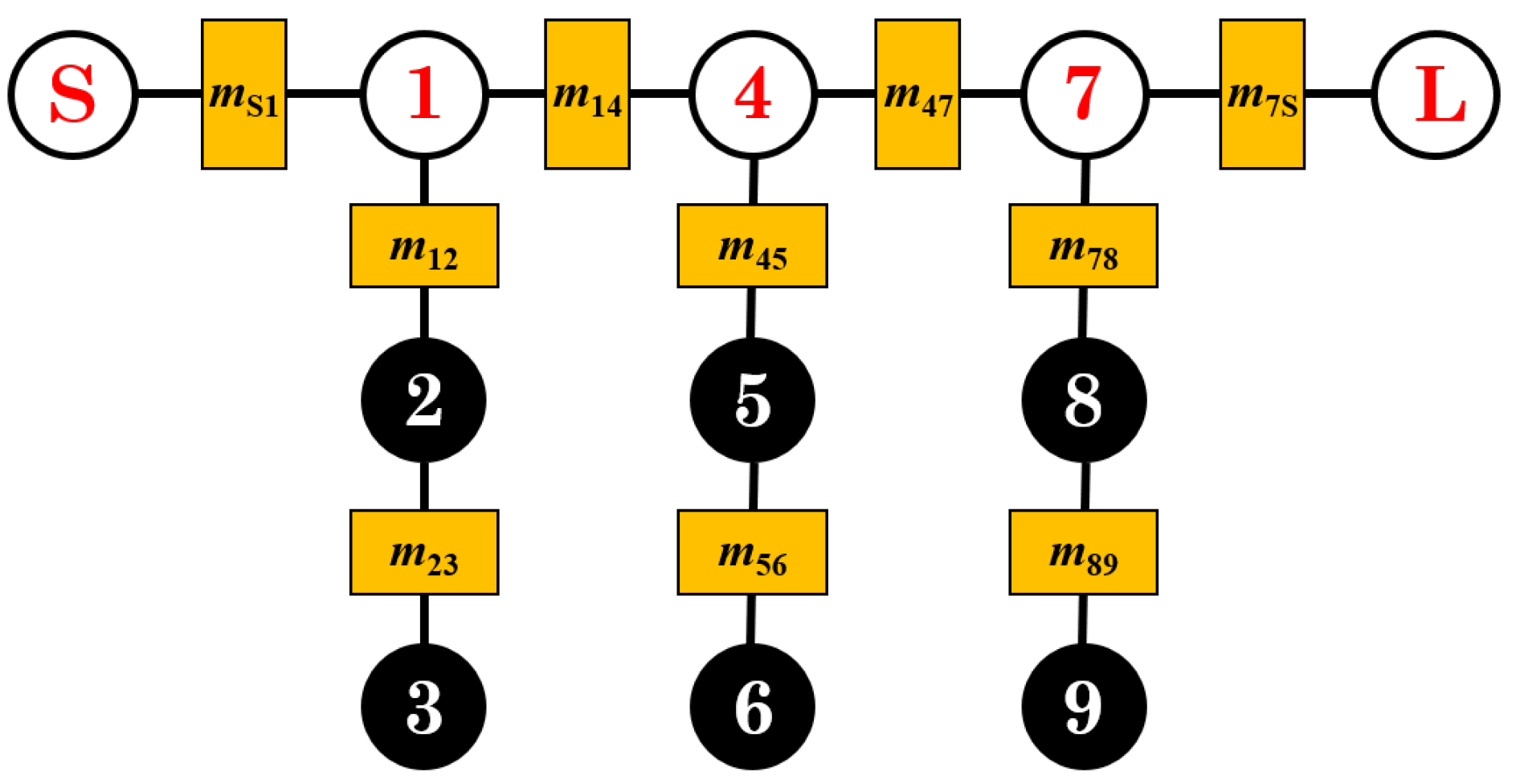
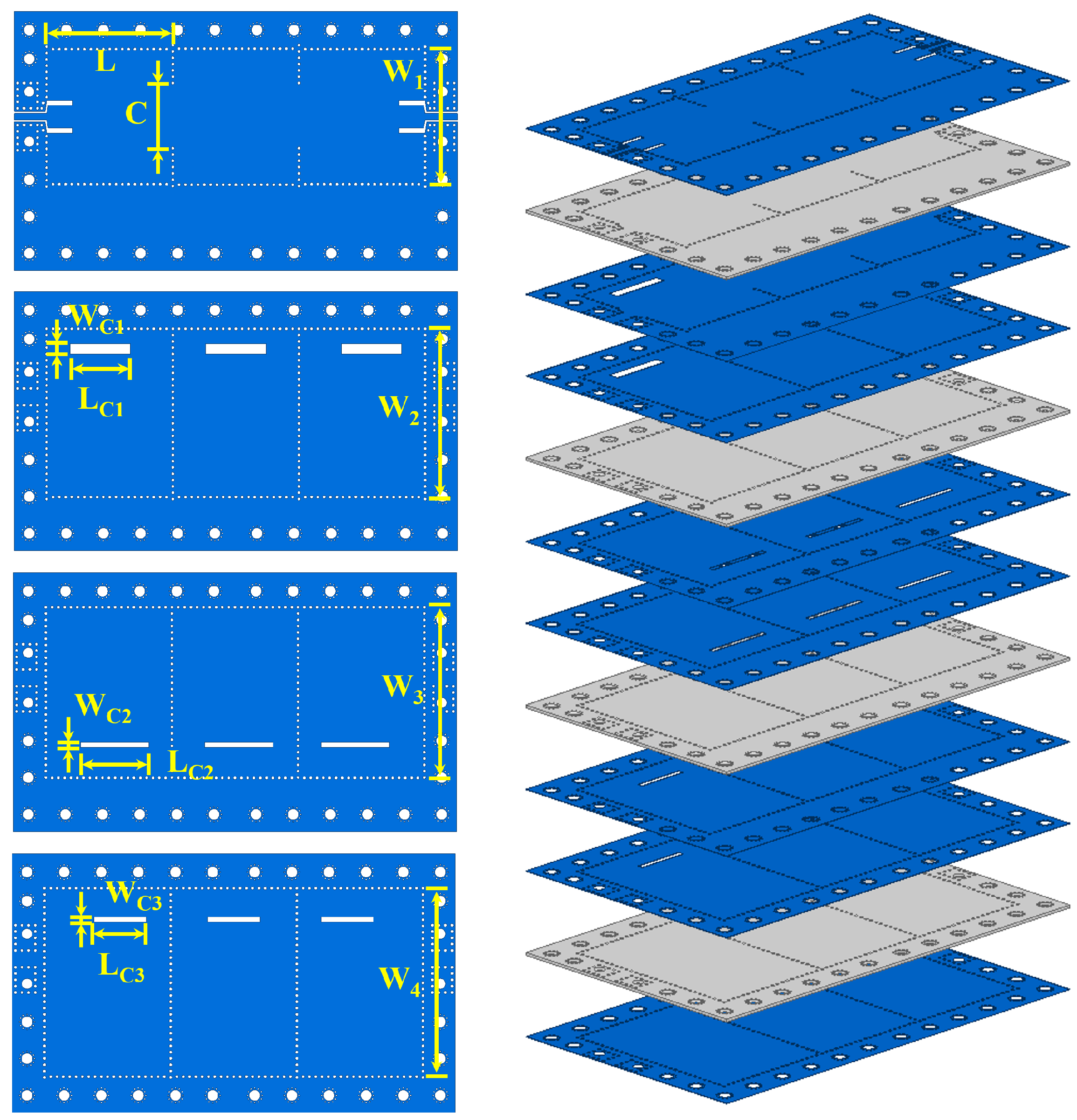
In this section, we synthesize and design two multi-layer multiband filters. Using the coupling matrix, we extracted the theoretical frequency response and constructed the electromagnetic (EM) simulation model. Figure 1 illustrates the proposed structure of the designed third-order tri-band SIW filter, which consists of nine resonant cavities arranged in a multi-layer configuration. The horizontally distributed resonators share the same physical dimensions and are coupled through irises, while the vertically distributed resonators vary in size and are coupled via slots on the surface of the metal layer. Figure 2 displays the topology of this circuit prototype. Based on their frequency characteristics, the resonators can be categorized into two types: bandpass resonators, located along the main coupling path from the source to the load, which provide poles in the multiband response; and bandstop resonators, which create transmission zeros between adjacent operating bands. All bandpass resonators are coupled with one another, while bandstop resonators are only coupled vertically, with no coupling occurring horizontally. This multi-layer configuration significantly reduces the size of the filter. Additionally, due to the low profile characteristics of the SIW structure, variations in circuit thickness can be nearly disregarded.
In the proposed structure, the fundamental T E 101 mode of the SIW square cavity is mainly used, and the resonant frequency can be calculated as [24]
f T E 101 = c 2 μ r ε r 1 W e f f 2 + 1 L e f f 2
W e f f = W d 2 0.95 p
L e f f = L d 2 0.95 p
where ε r is the permittivity of the substrate, μ r is the relative permeability, and W and L are the width and length of the cavity, respectively. p is the via hole pitch, and d is the via hole diameter. For quantitative analysis, the SIW resonant cavity can be equivalent to a series R L C circuit, and the specific values can be extracted with the help of EM simulation software as follows [25]:
R = R e ( Z i n )
L = 1 4 π d ( I m ( Z i n ) ) d f f = f 0
C = 1 4 π 2 f 2 L f = f 0
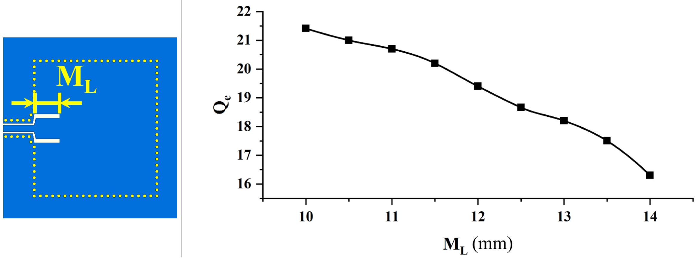
For the designed structure, the external quality factors ( Q e ) can be calculated using the following Equation [24]:
Q e = ω 0 τ S 11 ( ω 0 ) 4
where τ S 11 is the group delay at the resonant frequency ω 0 . With the single-port excitation, the variation in the Q e value with the input matching structure can be obtained as Figure 3.
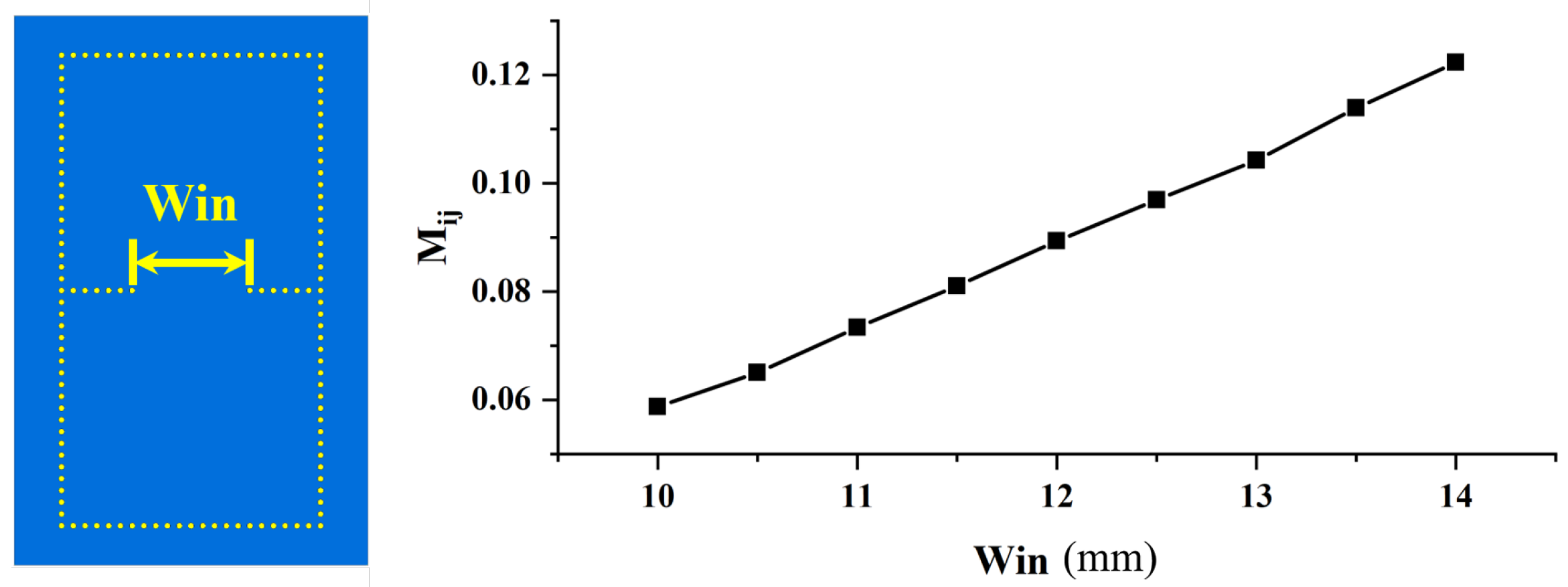
The coupling between resonators can be classified into synchronous tuning and asynchronous tuning, depending on the resonant frequencies of the coupled resonator pairs. If the resonant frequencies of the coupled resonators are identical, the coupling is termed synchronous tuning. Conversely, if the resonant frequencies differ, it is classified as asynchronous tuning. For the horizontally distributed resonators, which share the same dimensions and resonant frequencies, the coupling falls under synchronous tuning. The coupling coefficient can be calculated as follows [25]:
M i j = f i 2 f j 2 f i 2 + f j 2
Figure 4 exhibits the curve of the extracted coupling coefficient as the iris size changes. It can be seen that the coupling coefficient is positively correlated with the iris size.
For the vertically distributed resonators, they have different dimensions and resonant frequencies, which belongs to asynchronous tuning [25], and the coupling coefficient can be calculated as in Equation (9).
m i j = 1 2 f 0 i f 0 j + f 0 j f 0 i f i 2 f j 2 f i 2 + f j 2 2 f 0 i 2 f 0 j 2 f 0 i 2 + f 0 j 2 2
The coupling coefficient for vertical coupling is primarily influenced by the length, width, and position of the coupling slot. We extract the coupling coefficients under different conditions. As illustrated in Figure 5, the coupling coefficient shows a positive correlation with both the length and width of the coupling slot. Additionally, as the coupling slot is positioned closer to the edge of the resonant cavity, the coupling coefficient increases. This behavior can be explained by the field distribution in an SIW rectangular resonant cavity. The electric field strength is indicated by color gradient. It can be found that the electric field is strongest at the center, while the magnetic field is strongest at the edges. Since the vertical integration coupling window relies on magnetic coupling, enlarging the coupling slot and moving it closer to the region of the strong magnetic field enhances the coupling strength.
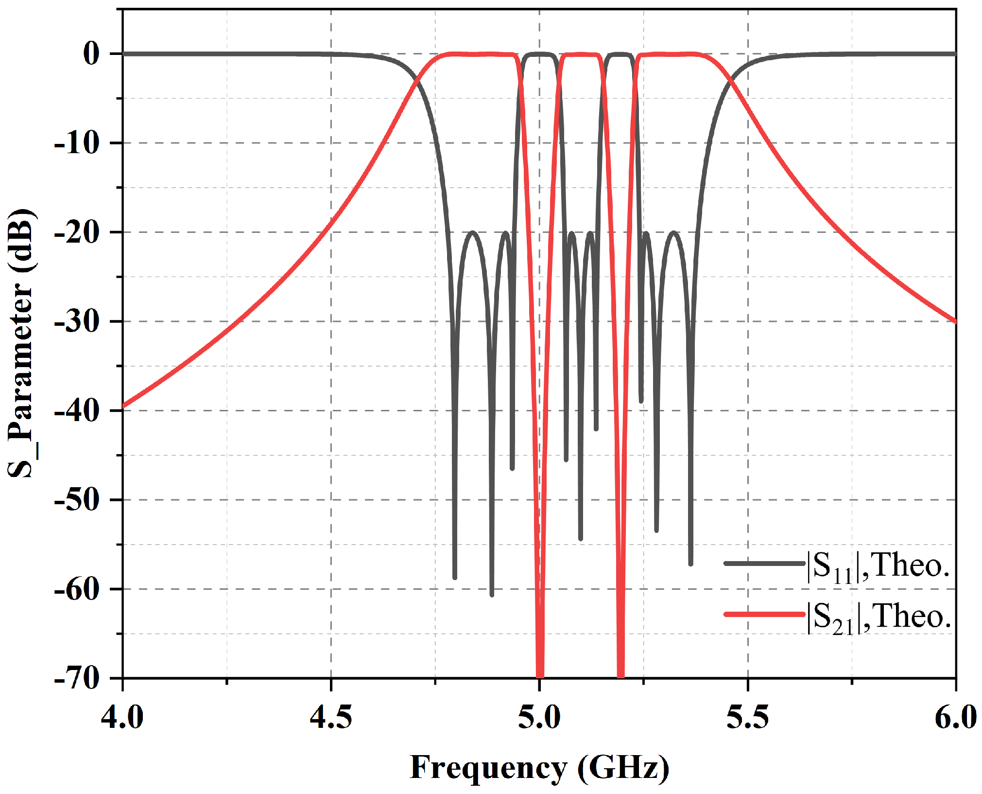
Through the parameter extraction process, the coupling matrix of the designed third-order tri-band SIW filter can be calculated as in Equation (10), and the related theoretical frequency response can be simulated as in Figure 6.
M = 0 0.0420 0 0 0 0 0 0 0 0 0 0.0420 0.0028 0.0676 0 0.0774 0 0 0 0 0 0 0 0.0676 0.0053 0.0377 0 0 0 0 0 0 0 0 0 0.0377 0.0154 0 0 0 0 0 0 0 0 0.0774 0 0 0.0028 0.0676 0 0.0774 0 0 0 0 0 0 0 0.0676 0.0053 0.0377 0 0 0 0 0 0 0 0 0 0.0377 0.0154 0 0 0 0 0 0 0 0 0.0774 0 0 0.0028 0.0676 0 0.0420 0 0 0 0 0 0 0 0.0676 0.0053 0.0377 0 0 0 0 0 0 0 0 0 0.0377 0.0154 0 0 0 0 0 0 0 0 0.0420 0 0 0
To further highlight the flexibility of the structure, here, we provide the second example of a third-order quad-band SIW filter. The EM model of this circuit is shown in Figure 7.
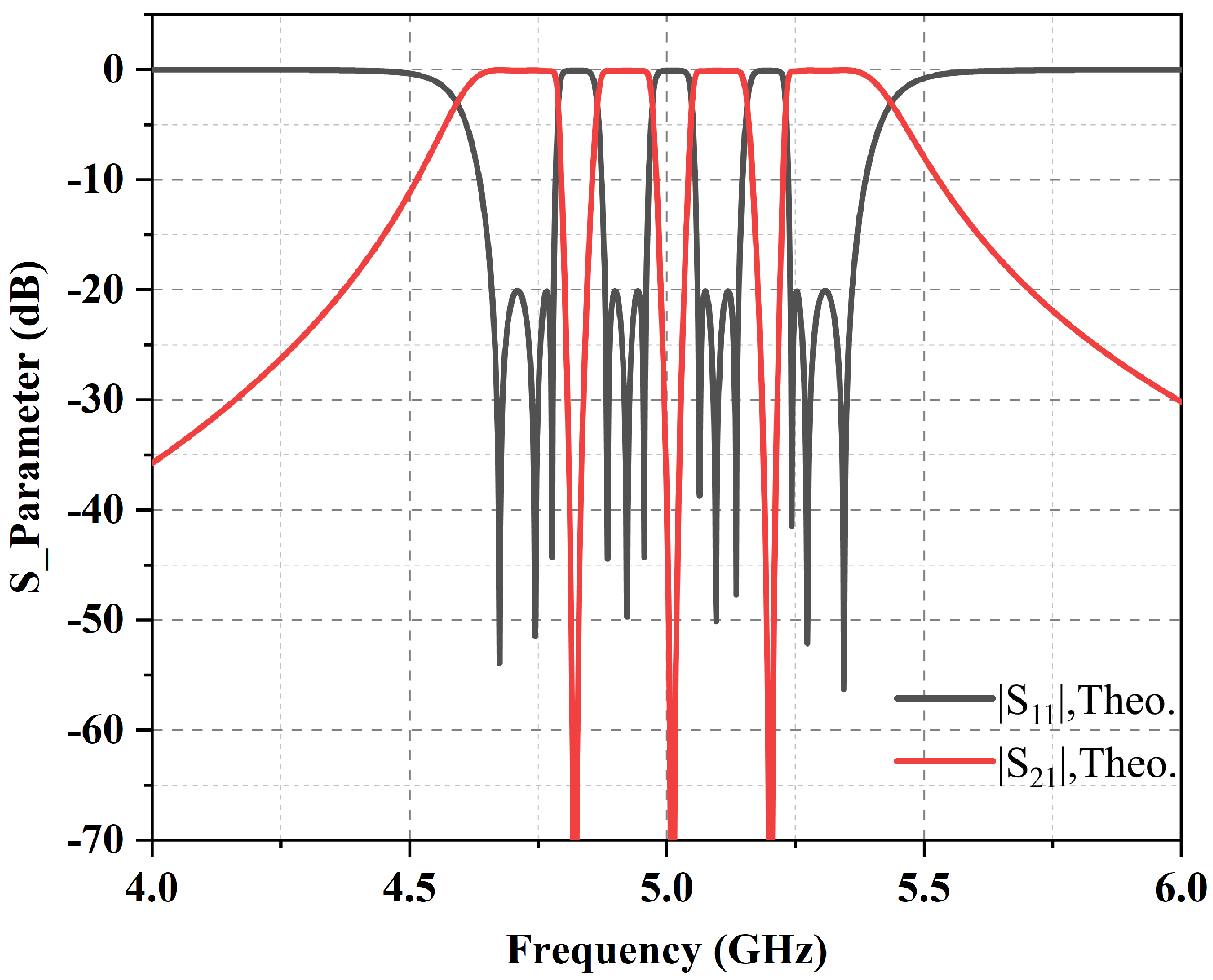
Compared with the third-order case, the fourth-order case adds an extra layer of structure in the vertical direction. Using a similar analysis approach, the coupling matrix of the designed third-order quad-band SIW filter can be calculated as in (11), and the theoretical frequency response can be simulated as in Figure 8.
M = 0 0.0434 0 0 0 0 0 0 0 0 0 0 0 0 0.0434 0.0017 0.0813 0 0 0.0826 0 0 0 0 0 0 0 0 0 0.0813 0.0019 0.0611 0 0 0 0 0 0 0 0 0 0 0 0 0.0611 0.0042 0.0449 0 0 0 0 0 0 0 0 0 0 0 0 0.0449 0.0074 0 0 0 0 0 0 0 0 0 0 0.0826 0 0 0 0.0017 0.0813 0 0 0.0826 0 0 0 0 0 0 0 0 0 0.0813 0.0019 0.0611 0 0 0 0 0 0 0 0 0 0 0 0 0.0611 0.0042 0.0449 0 0 0 0 0 0 0 0 0 0 0 0 0.0449 0.0074 0 0 0 0 0 0 0 0 0 0 0.0826 0 0 0 0.0017 0.0813 0 0 0.0434 0 0 0 0 0 0 0 0 0 0.0813 0.0019 0.0611 0 0 0 0 0 0 0 0 0 0 0 0 0.0611 0.0042 0.0449 0 0 0 0 0 0 0 0 0 0 0 0 0.0449 0.0074 0 0 0 0 0 0 0 0 0 0 0.0434 0 0 0 0

3. Experimental Validation

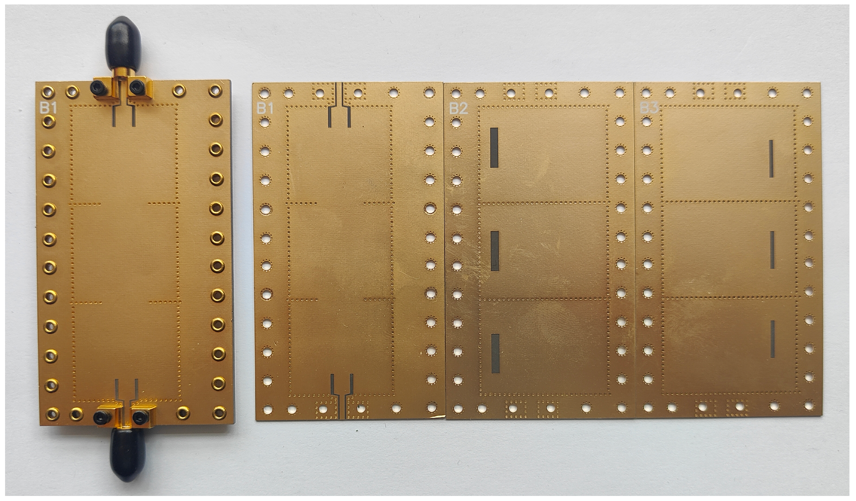
In this study, we fabricated and measured the designed multiband filters in Section 2. For the implementation of the designed circuit prototype, the RT/duroid 5880 substrate with ε r = 2.2 , tan δ = 0.0009 , and h = 0.508 mm was used here. All the circuits were manufactured using standard PCB processing techniques. Nickel–gold plating was applied to the surfaces to enhance oxidation resistance. Multi-layer circuits were aligned using positioning pins and secured through riveting for stability and durability. Figure 9 exhibits a photograph of the fabricated third-order tri-band SIW filter. The overall size of the core circuit was about 1.22 λ 0 × 0.58 λ 0 . The S-parameters were measured using a vector network analyzer R&S ZNA with a frequency step of 1 MHz. The calibration standard was Through Open Short Match (TOSM). The RF signal was fed through a 2.92 mm connector into the SMA connector.
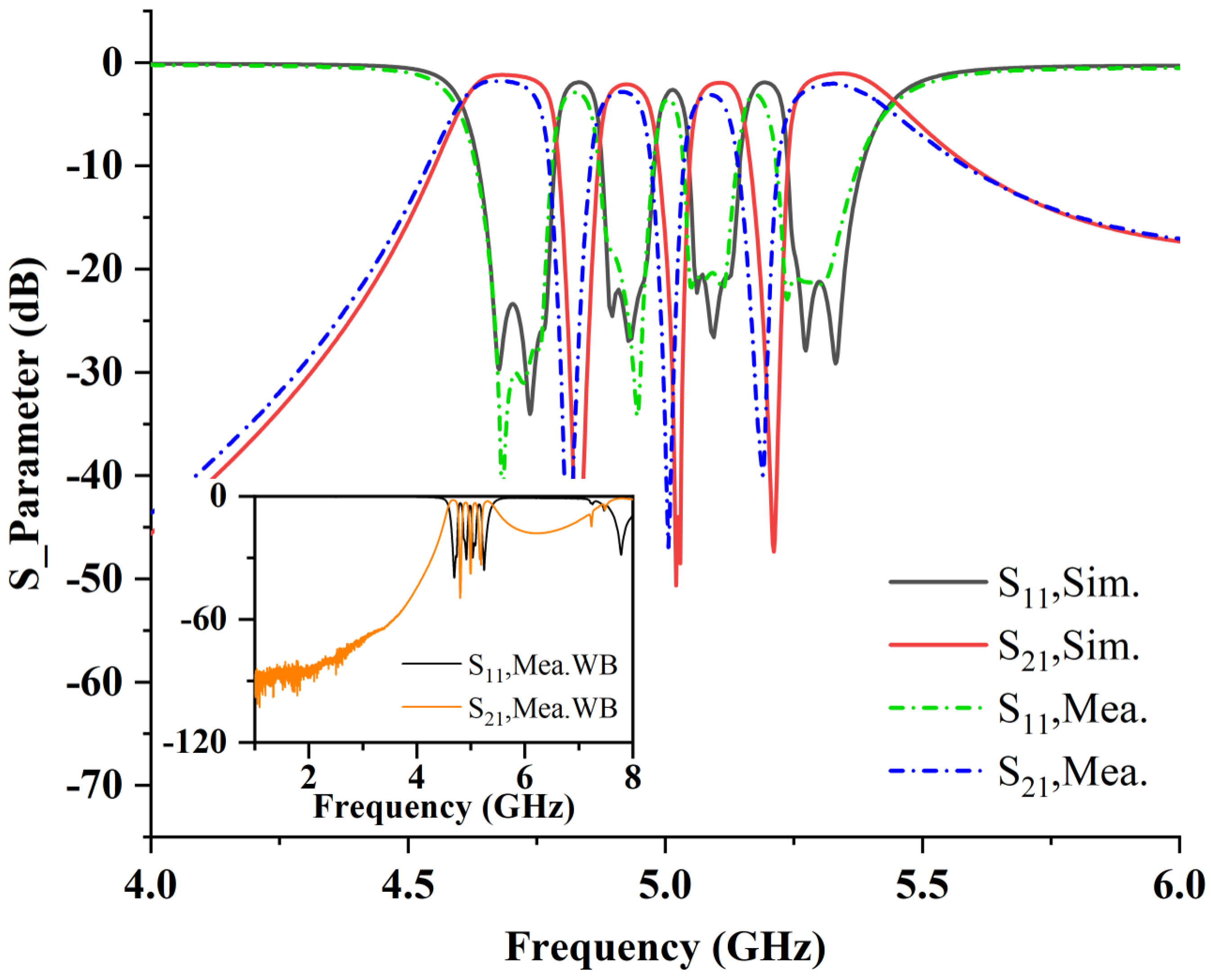
Figure 10 exhibits the simulated and measured S-parameters of the fabricated third-order tri-band SIW filter. All nine poles can be observed, which shows good agreement with the theoretical frequency response. For the measured results, the first passband is centered at 4.81 GHz with a 3 dB fractional bandwidth (FBWs) of 4.48%, the second passband is centered at 5.08 GHz with a FBW of 1.84%, and the third passband is centered at 5.35 GHz with a FBW of 4.71%. The minimum measured insertion losses of three bands were −1.41 dB, −2.64 dB, and −1.39 dB, respectively, while the return loss was better than 20 dB for all of the operating bands. The maximum isolation between the adjacent frequency bands was 52.41 dB and 67.56 dB, respectively. The wideband frequency responses were measured with a step size of 5 MHz, as an illustration of Figure 10. An additional resonant point can be observed around 8 GHz, which is primarily attributed to higher-order modes.
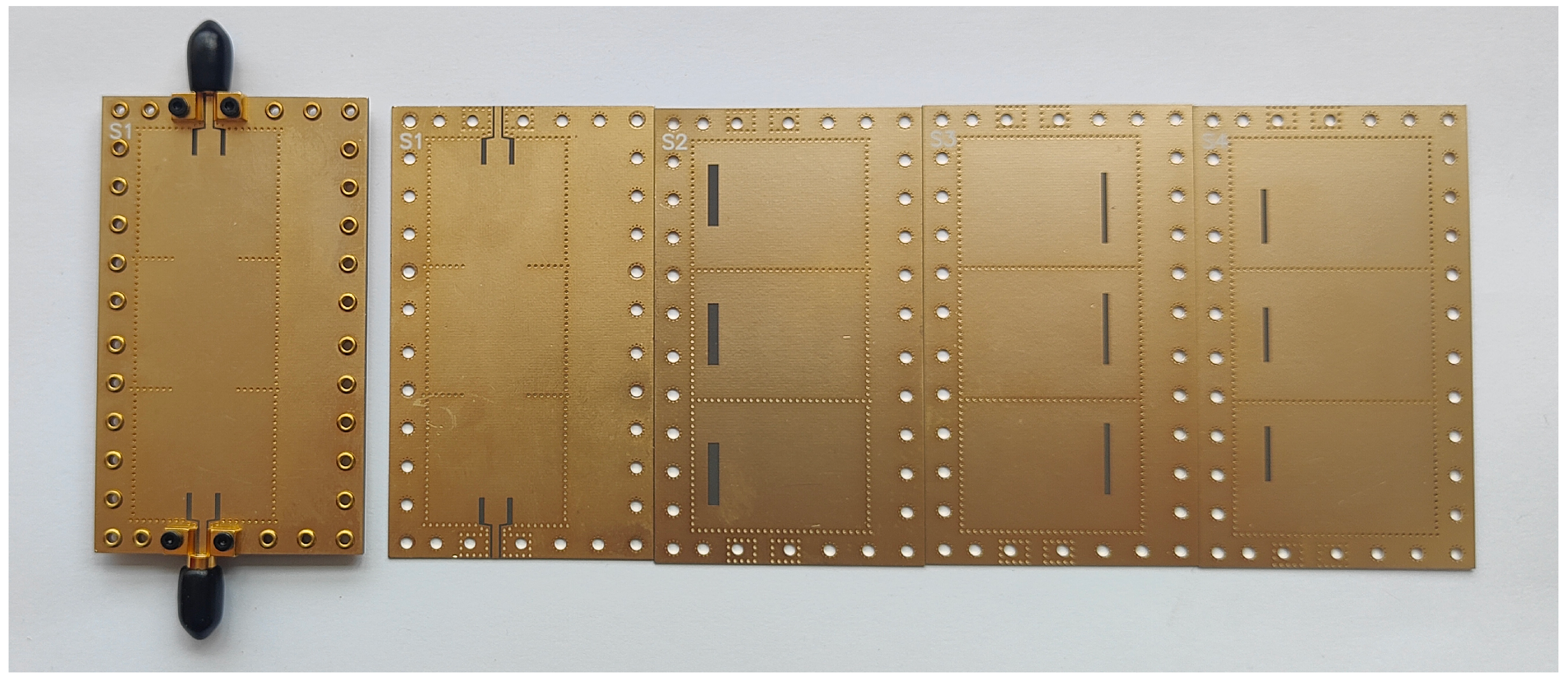
Figure 11 exhibits a photograph of the fabricated third-order quad-band SIW filter. The overall size of the core circuit was about 1.18 λ 0 × 0.61 λ 0 . Figure 12 exhibits the S-parameters of the fabricated third-order quad-band SIW filter with eleven poles observed. The first passband is centered at 4.67 GHz with a 3 dB fractional bandwidth FBW of 3.63%, the second passband is centered at 4.91 GHz with a FBW of 1.91%, the third passband is centered at 5.09 GHz with a FBW of 1.61%, and the forth passband is centered at 5.34 GHz with a FBW of 3.91%. The minimum measured insertion losses of the four bands were −1.64 dB, −2.66 dB, −2.96 dB, and −1.87 dB, respectively. The return loss was better than 18 dB for all of the operating bands. The maximum isolation between the adjacent frequency bands was 55.06 dB, 46.29 dB, and 40.26 dB, respectively. Slight frequency deviation can be observed, but it is within an acceptable range. This can be attributed to errors introduced in the processing and assembly processes, as well as discontinuities arising from the SMA connector installation process.
A performance comparison is presented in Table 1, highlighting the advantages of the multiband SIW filter designed in this study, particularly in terms of in-band isolation. The filter maintains excellent suppression across all adjacent passbands, which is crucial for preventing signal crosstalk and improving linearity in multiband applications. Additionally, the introduction of a multi-layer structure effectively reduces the circuit size, offering significant potential for achieving high-density integration within systems. In summary, the proposed multiband filter excels in both miniaturization and high isolation, facilitating a compact design for front-end systems. It is especially suitable for applications such as Wi-Fi, the Internet of Things, and satellite communications. Given the rapid development and widespread adoption of 5G multiband cooperative communication technology, this filter demonstrates substantial application potential, effectively enhancing communication quality and overall system performance.

4. Discussion

In this work, we focused on the multiband SIW bandpass filter with a multi-layer configuration. Based on the measured results, we achieve good in-band isolation between all passbands. To further improve the roll-off of the upper and lower sidebands, additional transmission zeros can be introduced through cross-coupling technology. For a fourth-order tri-band bandpass filter, the topology incorporating cross-coupling is illustrated in Figure 13. By defining the coupling matrix as shown in (12), we can simulate the theoretical frequency response. The results indicate a significant improvement in the out-of-band roll-off of the multiband filter response. Detailed circuit design and measurements will be addressed in future work. Moreover, since all SIW resonant cavities can be equivalently represented as RLC parallel circuits, integrating reconfigurable components allows for adjustments in center frequency and bandwidth, thereby enhancing the flexibility of multiband filter responses. This presents an exciting research opportunity and will be a major focus of our future investigations [30,31,32,33].
M = 0 0.0371 0 0 0 0 0 0 0 0 0 0 0 0 0.0371 0.0036 0.0522 0 0.0551 0 0 0 0 0 0 0 0 0 0 0.0522 0.0045 0.0496 0 0 0 0 0 0 0 0 0 0 0 0 0.0496 0.0085 0 0 0 0 0 0 0 0 0 0 0 0.0551 0 0 0.0036 0.0522 0 0.0483 0 0 0 0 0 0 0 0 0 0 0.0522 0.0045 0.0496 0 0 0 0 0 0 0 0 0 0 0 0 0.0496 0.0085 0 0 0 0 0 0 0 0 0 0 0 0.0483 0 0 0.0036 0.0522 0 0.0551 0 0 0 0 0 0 0 0 0 0 0.0522 0.0045 0.0496 0 0 0 0 0 0 0 0 0 0 0 0 0.0496 0.0085 0 0 0 0 0 0 0 0 0 0 0 0.0551 0 0 0.0036 0.0522 0 0.0371 0 0 0 0 0 0 0 0 0 0 0.0522 0.0045 0.0496 0 0 0 0 0 0 0 0 0 0 0 0 0.0496 0.0085 0 0 0 0 0 0 0 0 0 0 0 0.0371 0 0 0

5. Conclusions

This article presents a miniaturized multiband SIW bandpass filter structure with a multi-layer configuration. The coupling matrix was calculated to accurately characterize the coupling relationships between resonators, and the influence of slot size on vertical coupling strength was analyzed. To validate the filter model, we fabricated third-order tri-band and quad-band SIW filters. The proposed structure demonstrates significant advantages in circuit size and in-band isolation, making it well suited for multiband communication applications. Additionally, it serves as a valuable reference for designing complex multiband filters, with potential applications in multiband wireless communications, including cellular networks, Wi-Fi, the Internet of Things, and satellite communications.

Author Contributions

Conceptualization, Y.W.; methodology, Y.W. and Y.Z.; formal analysis, Y.W. and Y.Z.; investigation, Y.W. and Y.Z.; writing—original draft preparation, Y.W., Y.Z., K.M. and K.S.Y.; writing—review and editing, Y.W., Y.Z., K.M. and K.S.Y.; supervision, K.M. and K.S.Y.; project administration, K.M. and K.S.Y. All authors have read and agreed to the published version of the manuscript.

Funding

This research was funded by the National Natural Science Foundation of China under grants 62301358 and 62341409, and in part by the China Postdoctoral Science Foundation under grant 2024T170638.

Data Availability Statement

All data are included within the manuscript.

Conflicts of Interest

The authors declare no conflicts of interest.

References

  1. Pradhan, N.C.; Koziel, S.; Barik, R.K.; Pietrenko-Dabrowska, A.; Karthikeyan, S.S. Miniaturized dual-band SIW-based bandpass filters using open-loop ring resonators. Electronics 2023, 12, 3974. [Google Scholar] [CrossRef]
  2. Huang, X.; Liu, Z. Low-cost W-band dual-mode SIW bandpass filters using commercially available printed-circuit-board technology. Electronics 2023, 12, 3624. [Google Scholar] [CrossRef]
  3. Nwajana, A.O.; Obi, E.R. A review on SIW and its applications to microwave components. Electronics 2022, 11, 1160. [Google Scholar] [CrossRef]
  4. Shah, M.; Cheema, H.M.; Abbasi, Q.H. Substrate Integrated Waveguide Antenna System for 5G In-Band Full Duplex Applications. Electronics 2021, 10, 2456. [Google Scholar] [CrossRef]
  5. Chen, X.P.; Wu, K. Substrate integrated waveguide filters: Design techniques and structure innovations. IEEE Microw. Mag. 2014, 15, 121–133. [Google Scholar] [CrossRef]
  6. Zhu, F.; Wu, Y.; Chu, P.; Luo, G.Q.; Wu, K. Compact dual-band filtering baluns using perturbed substrate integrated waveguide circular cavities. IEEE Microw. Wirel. Technol. Lett. 2023, 33, 663–666. [Google Scholar] [CrossRef]
  7. Niembro-Martin, A.; Nasserddine, V.; Pistono, E.; Issa, H.; Franc, A.L.; Vuong, T.P.; Ferrari, P. Slow-wave substrate integrated waveguide. IEEE Trans. Microw. Theory Tech. 2014, 62, 1625–1633. [Google Scholar] [CrossRef]
  8. George, J.M.; Raghavan, S. A design of miniaturized SIW-based band-pass cavity filter. In Proceedings of the 2017 International Conference on Communication and Signal Processing (ICCSP), Chennai, India, 6–8 April 2017; pp. 622–624. [Google Scholar]
  9. Bertrand, M.; Pistono, E.; Kaddour, D.; Puyal, V.; Ferrari, P. A filter synthesis procedure for slow wave substrate-integrated waveguide based on a distribution of blind via holes. IEEE Trans. Microw. Theory Tech. 2018, 66, 3019–3027. [Google Scholar] [CrossRef]
  10. Jin, H.; Wang, K.; Guo, J.; Ding, S.; Wu, K. Slow-wave effect of substrate integrated waveguide patterned with microstrip polyline. IEEE Trans. Microw. Theory Tech. 2016, 64, 1717–1726. [Google Scholar] [CrossRef]
  11. Ding, Y.; Wu, K. Miniaturized hybrid ring circuits using T-type folded substrate integrated waveguide (TFSIW). In Proceedings of the 2009 IEEE MTT-S International Microwave Symposium Digest, Boston, MA, USA, 7–12 June 2009; pp. 705–708. [Google Scholar]
  12. Chien, H.Y.; Shen, T.M.; Huang, T.Y.; Wang, W.H.; Wu, R.B. Miniaturized bandpass filters with double-folded substrate integrated waveguide resonators in LTCC. IEEE Trans. Microw. Theory Tech. 2009, 57, 1774–1782. [Google Scholar] [CrossRef]
  13. Zhang, C.A.; Cheng, Y.J.; Fan, Y. Quadri-folded substrate integrated waveguide cavity and its miniaturized bandpass filter applications. Prog. Electromagn. Res. C 2011, 23, 1–14. [Google Scholar] [CrossRef]
  14. Zhu, L.; Yang, S.; Cao, T.; Huang, Y.; Ji, T.; Wang, J.; Xu, J.; Yu, Z.; Zhou, J.; Hong, W. A design method to realize manufacture-friendly millimeter-wave folded substrate integrated waveguide bandpass filters. IEEE Trans. Circuits Syst. II Express Briefs 2022, 70, 979–983. [Google Scholar] [CrossRef]
  15. Gu, L.; Dong, Y. Compact half-mode SIW filter with high selectivity and improved stopband performance. IEEE Microw. Wirel. Components Lett. 2022, 32, 1039–1042. [Google Scholar] [CrossRef]
  16. Weng, X.; Xu, K.D.; Fan, H. Wideband bandpass filters based on eighth-mode substrate integrated waveguide and microstrip resonators. IEEE Trans. Circuits Syst. II Express Briefs 2023, 70, 2375–2379. [Google Scholar] [CrossRef]
  17. Azad, A.R.; Mohan, A. A compact sixteenth-mode substrate integrated waveguide bandpass filter with improved out-of-band performance. Microw. Opt. Technol. Lett. 2017, 59, 1728–1733. [Google Scholar] [CrossRef]
  18. Chen, X.P.; Wu, K.; Li, Z.L. Dual-band and triple-band substrate integrated waveguide filters with Chebyshev and quasi-elliptic responses. IEEE Trans. Microw. Theory Tech. 2007, 55, 2569–2578. [Google Scholar] [CrossRef]
  19. Guo, X.; Zhu, L.; Wu, W. Design method for multiband filters with compact configuration in substrate integrated waveguide. IEEE Trans. Microw. Theory Tech. 2018, 66, 3011–3018. [Google Scholar] [CrossRef]
  20. Zhou, K.; Zhou, C.X.; Wu, W. Substrate-integrated waveguide dual-band filters with closely spaced passbands and flexibly allocated bandwidths. IEEE Trans. Components Packag. Manuf. Technol. 2018, 8, 465–472. [Google Scholar] [CrossRef]
  21. Xie, H.W.; Zhou, K.; Zhou, C.X.; Wu, W. Substrate-integrated waveguide triple-band bandpass filters using triple-mode cavities. IEEE Trans. Microw. Theory Tech. 2018, 66, 2967–2977. [Google Scholar] [CrossRef]
  22. Zhou, K.; Zhou, C.X.; Wu, W. Resonance characteristics of substrate-integrated rectangular cavity and their applications to dual-band and wide-stopband bandpass filters design. IEEE Trans. Microw. Theory Tech. 2017, 65, 1511–1524. [Google Scholar] [CrossRef]
  23. Zhou, K.; Zhou, C.X.; Xie, H.W.; Wu, W. Synthesis design of SIW multiband bandpass filters based on dual-mode resonances and split-type dual-and triple-band responses. IEEE Trans. Microw. Theory Tech. 2018, 67, 151–161. [Google Scholar] [CrossRef]
  24. Hong, J.S.G.; Lancaster, M.J. Microstrip Filters for RF/Microwave Applications; John Wiley & Sons: Hoboken, NJ, USA, 2004. [Google Scholar]
  25. Wu, Y.; Ma, K.; Wang, Y. Coupling matrix design of compact multiband cascaded trisection bandpass filters. IEEE Trans. Circuits Syst. II Express Briefs 2022, 69, 2762–2766. [Google Scholar] [CrossRef]
  26. Zhang, X.Y.; Xue, Q.; Hu, B.J. Planar tri-band bandpass filter with compact size. IEEE Microw. Wirel. Components Lett. 2010, 20, 262–264. [Google Scholar] [CrossRef]
  27. Gao, L.; Zhang, X.Y.; Xue, Q. Compact tri-band bandpass filter using novel eight-mode resonator for 5G WiFi application. IEEE Microw. Wirel. Components Lett. 2015, 25, 660–662. [Google Scholar] [CrossRef]
  28. Esmaeili, M.; Bornemann, J. Substrate integrated waveguide triple-passband dual-stopband filter using six cascaded singlets. IEEE Microw. Wirel. Comp. Lett. 2014, 24, 439–441. [Google Scholar] [CrossRef]
  29. Liu, J.C.; Wang, J.W.; Zeng, B.H.; Chang, D.C. CPW-fed dual-mode double-square-ring resonators for quad-band filters. IEEE Trans. Microw. Theory Tech. 2010, 20, 142–144. [Google Scholar] [CrossRef]
  30. Borah, D.; Kalkur, T.S. A balanced dual-band tunable bandpass filter. In Proceedings of the 2018 International Applied Computational Electromagnetics Society Symposium (ACES), Denver, CO, USA, 24–29 March 2018. [Google Scholar]
  31. Gómez-García, R.; Guyette, A.C.; Psychogiou, D.; Naglich, E.J.; Peroulis, D. Quasi-elliptic multi-band filters with center-frequency and bandwidth tunability. IEEE Microw. Wirel. Comp. Lett. 2016, 26, 192–194. [Google Scholar] [CrossRef]
  32. Borah, D.; Kalkur, T.S. Tunable multiband balanced bandstop filter with high CMRR. Prog. Electromagn. Res. C 2019, 97, 1–13. [Google Scholar] [CrossRef]
  33. Borah, D.; Kalkur, T.S. Ultra-compact balanced multiband fully reconfigurable bandstop filter. Prog. Electromagn. Res. C 2020, 100, 133–143. [Google Scholar] [CrossRef]
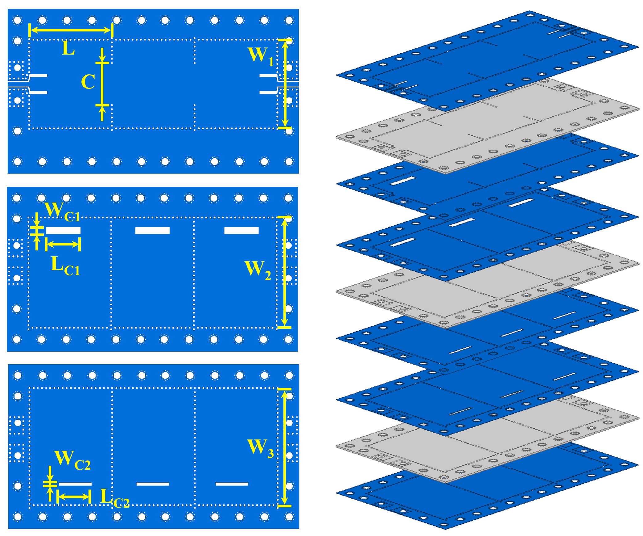
Figure 1. Structure of the designed third-order tri-band SIW filter ( L = 24 mm, W 1 = 25.7 mm, W 2 = 32 mm, W 3 = 34 mm, C = 12.2 mm, W C 1 = 2 mm, L C 1 = 10 mm, W C 2 = 1 mm, L C 2 = 9.5 mm).
Electronics 13 03834 g001
Figure 2. Topology structure of the designed third-order tri-band SIW filter.
Electronics 13 03834 g002
Figure 3. Variation in external quality factors with the input matching structure.
Electronics 13 03834 g003
Figure 4. Variation in coupling coefficients with the iris size of the coupling slot for horizontal coupling.
Electronics 13 03834 g004
Figure 5. Variation in coupling coefficients with the length, width, and position of the coupling slot for vertical coupling.
Electronics 13 03834 g005
Figure 6. Theoretical frequency response of the designed third-order tri-band SIW filter.
Electronics 13 03834 g006
Figure 7. Structure of the designed third-order quad-band SIW filter ( L = 24 mm, W 1 = 25.7 mm, W 2 = 32 mm, W 3 = 32.6 mm, W 4 = 35.8 mm, C = 12.2 mm, W C 1 = 2 mm, L C 1 = 11.5 mm, W C 2 = 1 mm, L C 2 = 13 mm, W C 3 = 1 mm, L C 3 = 10 mm).
Electronics 13 03834 g007
Figure 8. Theoretical frequency response of the designed third-order quad-band SIW filter.
Electronics 13 03834 g008
Figure 9. Photograph of fabricated third-order tri-band SIW filter.
Electronics 13 03834 g009
Figure 10. Simulated and measured S-parameters of fabricated third-order tri-band SIW filter.
Electronics 13 03834 g010
Figure 11. Photograph of fabricated third-order quad-band SIW filter.
Electronics 13 03834 g011
Figure 12. Simulated and measured S-parameters of fabricated third-order quad-band SIW filter.
Electronics 13 03834 g012
Figure 13. Topology structure of fourth-order tri-band filter with cross-coupling and related theoretical frequency response.
Electronics 13 03834 g013
Table 1. Comparisons with previous works on multiband bandpass filters.
RefOrderFrequency (GHz)3 dB FBWIL (dB)RL (dB)IsolationArea ( λ g 2 )
[26]2/2/21.84/2.45/2.984.9/3.5/5.70.9/1.6/0.8>15>300.22 × 0.27
[27]1/2/42.4/3.5/5.4511.6/6.7/17.81.1/1.2/1>15>35-
[21]3/3/313/14/154.06/3.31/2.821.71/1.80/2.2916.4/18.8/18>283.38 × 1.19
[28]3/2/29.7/10.8/11.84.01/3.44/3.320.33/0.45/0.3>10>104.58 × 1.53
Filter I3/3/34.81/5.08/5.354.48/1.84/4.711.41/2.64/1.39>20 dB52.41/67.561.18 × 0.58
[23]2/2/2/211.63/12.47/1.71/1.68/0.89/1.27/>15>251.47 × 1.06
13.51/14.351.38/1.221.45/1.36
[29]2/2/2/20.95/1.26/6.7/5.4/2.18/2.09/>10>250.5 × 0.5
1.89/2.2912/15.31.40/0.93
Filter II3/3/3/34.67/4.91/3.63/1.91/1.64/2.66/>1855.06/46.29/
40.26
1.18 × 0.61
5.09/5.341.61/3.912.96/1.87
Disclaimer/Publisher’s Note: The statements, opinions and data contained in all publications are solely those of the individual author(s) and contributor(s) and not of MDPI and/or the editor(s). MDPI and/or the editor(s) disclaim responsibility for any injury to people or property resulting from any ideas, methods, instructions or products referred to in the content.