

Miniaturized Multiband Substrate-Integrated Waveguide Bandpass Filters with Multi-Layer Configuration and High In-Band Isolation


Abstract
:1. Introduction
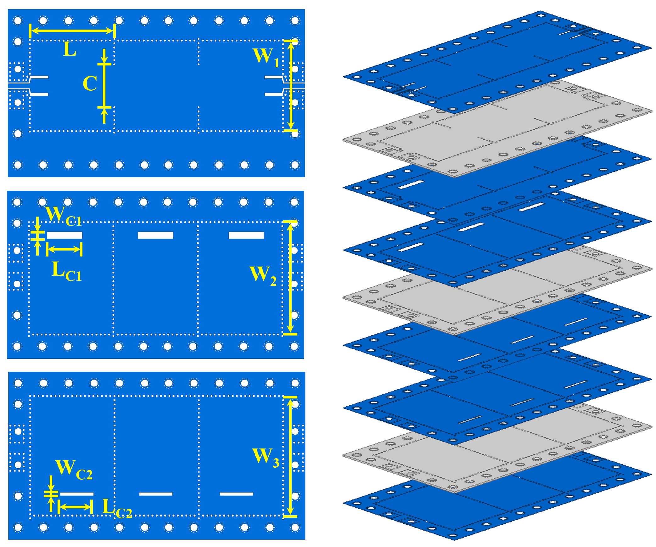
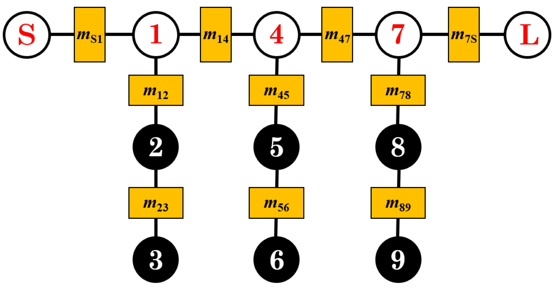
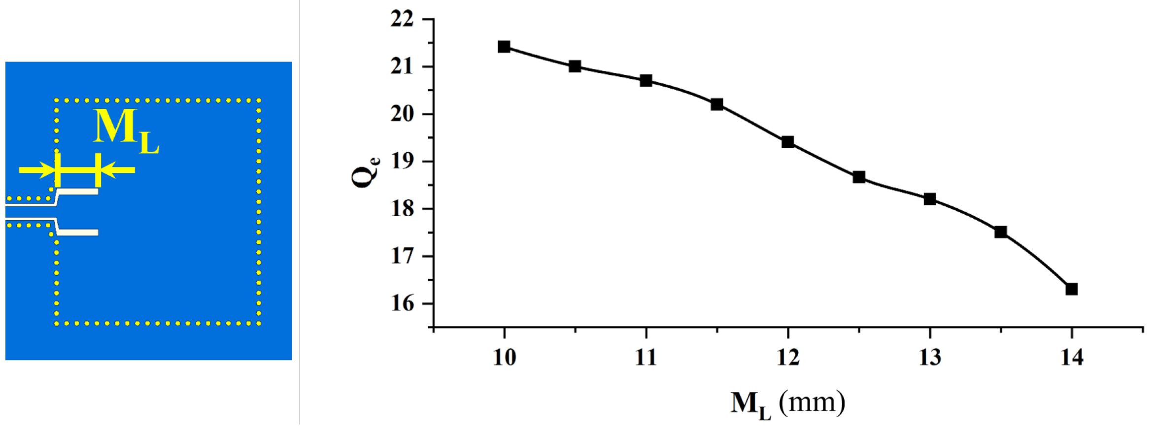
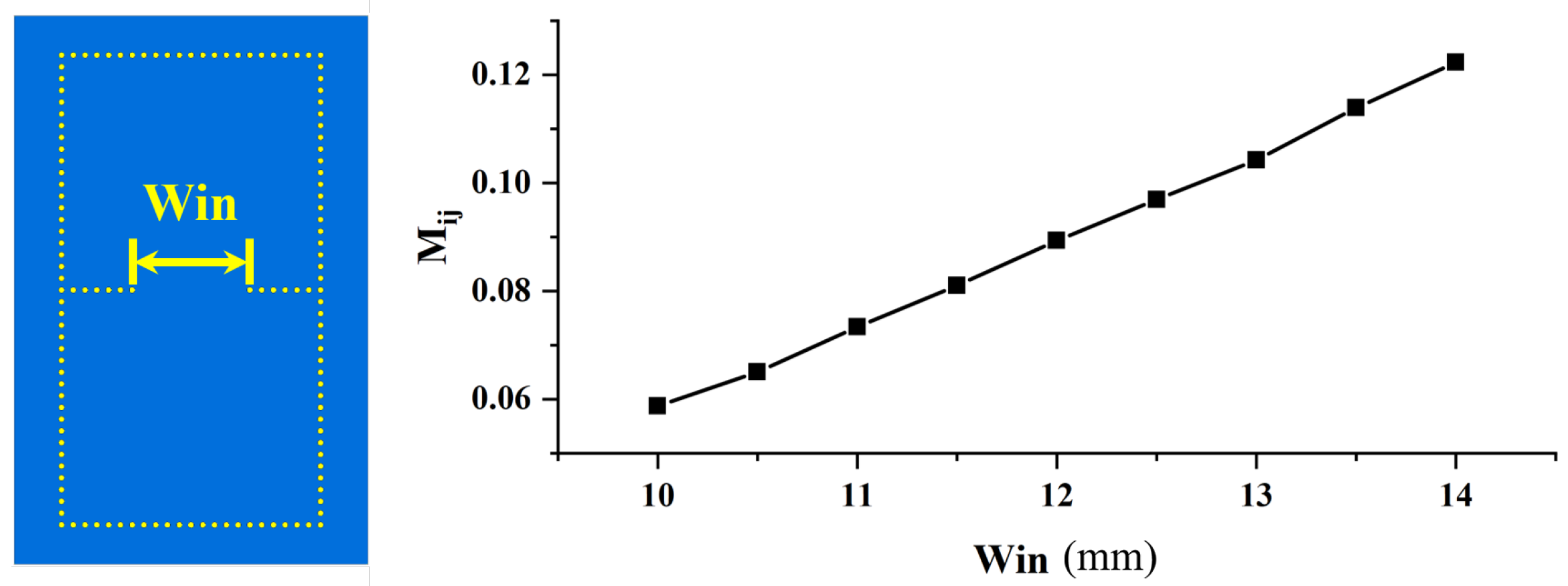
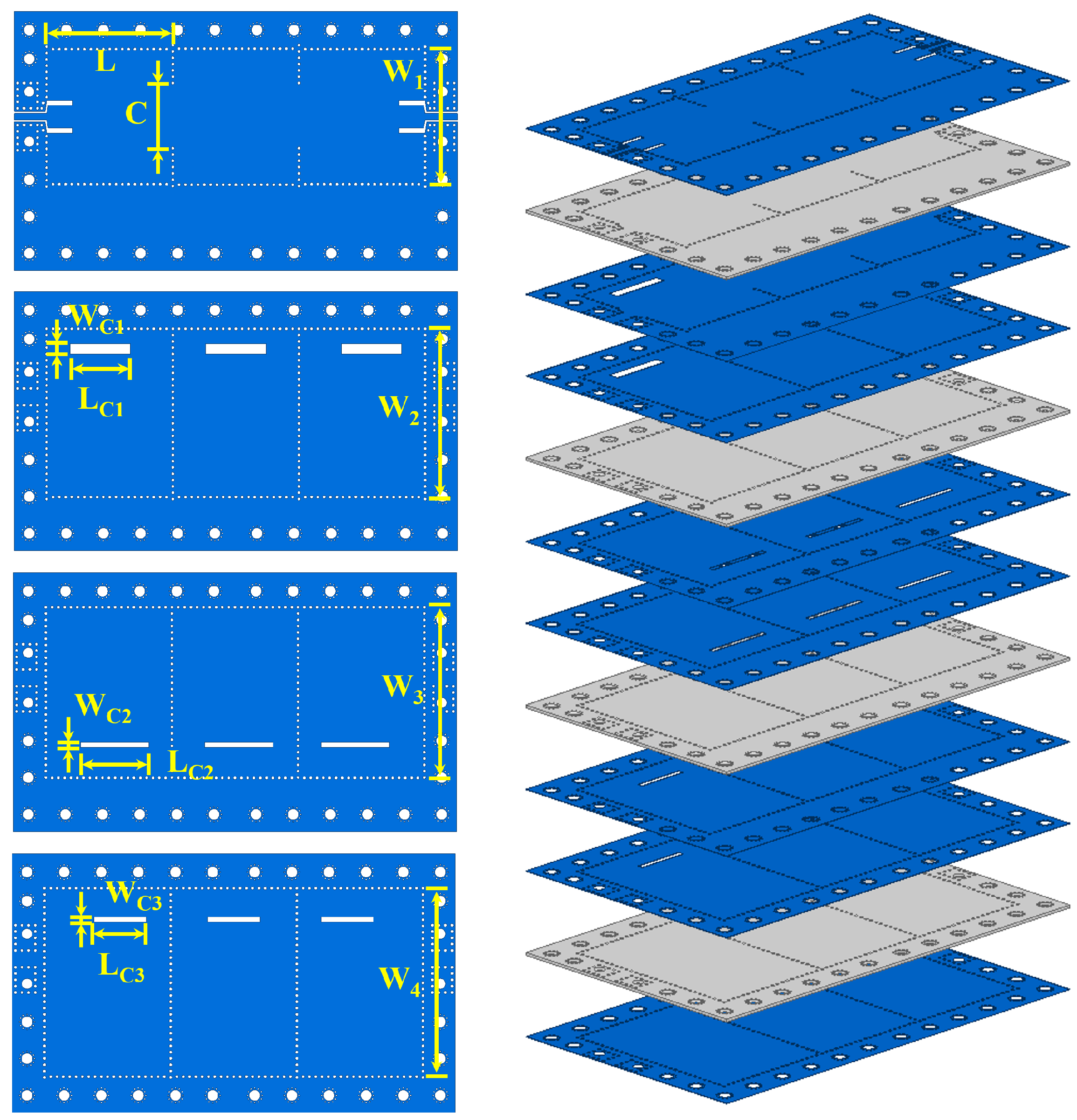
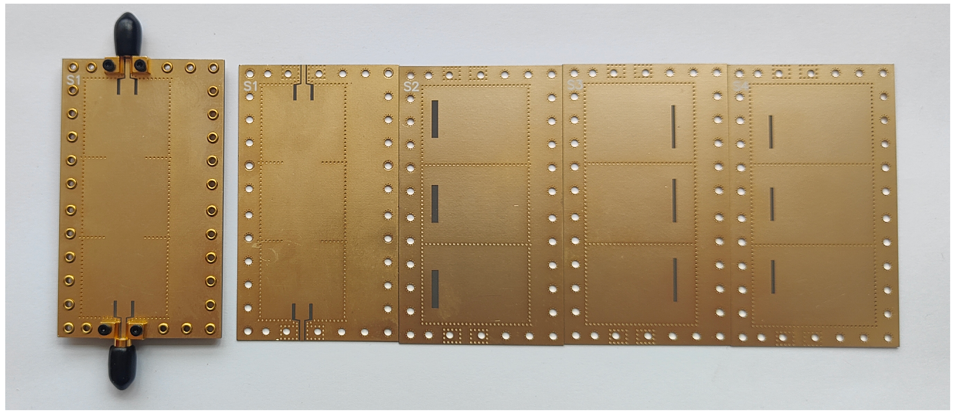
2. Filter Design
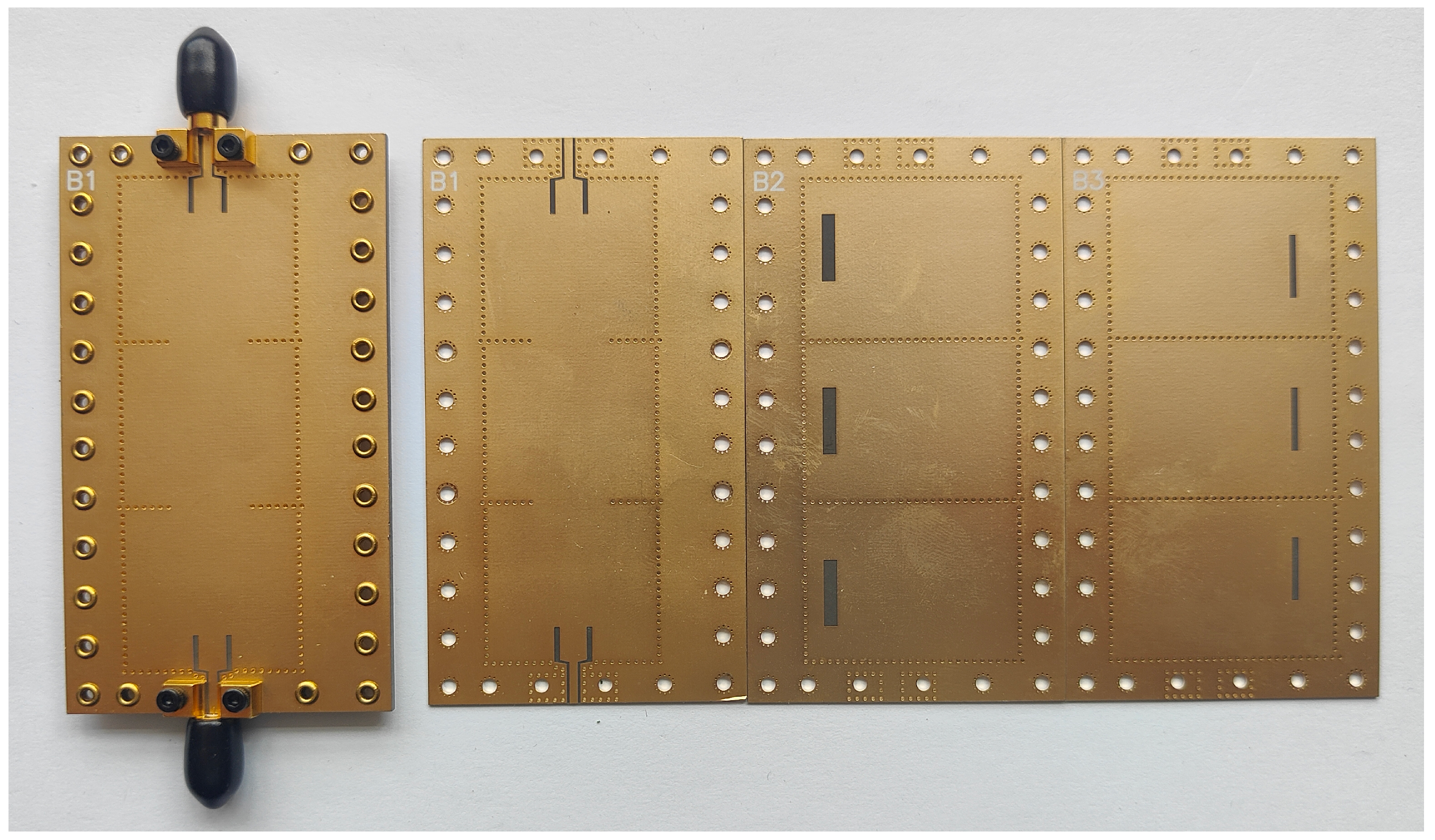
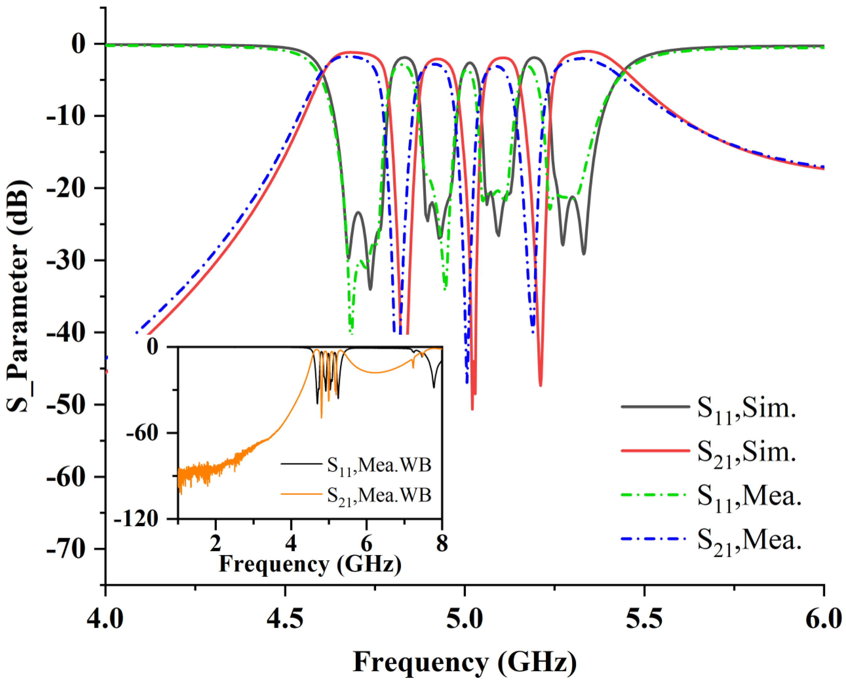
3. Experimental Validation
4. Discussion
5. Conclusions
Author Contributions
Funding
Data Availability Statement
Conflicts of Interest
References
- Pradhan, N.C.; Koziel, S.; Barik, R.K.; Pietrenko-Dabrowska, A.; Karthikeyan, S.S. Miniaturized dual-band SIW-based bandpass filters using open-loop ring resonators. Electronics 2023, 12, 3974. [Google Scholar] [CrossRef]
- Huang, X.; Liu, Z. Low-cost W-band dual-mode SIW bandpass filters using commercially available printed-circuit-board technology. Electronics 2023, 12, 3624. [Google Scholar] [CrossRef]
- Nwajana, A.O.; Obi, E.R. A review on SIW and its applications to microwave components. Electronics 2022, 11, 1160. [Google Scholar] [CrossRef]
- Shah, M.; Cheema, H.M.; Abbasi, Q.H. Substrate Integrated Waveguide Antenna System for 5G In-Band Full Duplex Applications. Electronics 2021, 10, 2456. [Google Scholar] [CrossRef]
- Chen, X.P.; Wu, K. Substrate integrated waveguide filters: Design techniques and structure innovations. IEEE Microw. Mag. 2014, 15, 121–133. [Google Scholar] [CrossRef]
- Zhu, F.; Wu, Y.; Chu, P.; Luo, G.Q.; Wu, K. Compact dual-band filtering baluns using perturbed substrate integrated waveguide circular cavities. IEEE Microw. Wirel. Technol. Lett. 2023, 33, 663–666. [Google Scholar] [CrossRef]
- Niembro-Martin, A.; Nasserddine, V.; Pistono, E.; Issa, H.; Franc, A.L.; Vuong, T.P.; Ferrari, P. Slow-wave substrate integrated waveguide. IEEE Trans. Microw. Theory Tech. 2014, 62, 1625–1633. [Google Scholar] [CrossRef]
- George, J.M.; Raghavan, S. A design of miniaturized SIW-based band-pass cavity filter. In Proceedings of the 2017 International Conference on Communication and Signal Processing (ICCSP), Chennai, India, 6–8 April 2017; pp. 622–624. [Google Scholar]
- Bertrand, M.; Pistono, E.; Kaddour, D.; Puyal, V.; Ferrari, P. A filter synthesis procedure for slow wave substrate-integrated waveguide based on a distribution of blind via holes. IEEE Trans. Microw. Theory Tech. 2018, 66, 3019–3027. [Google Scholar] [CrossRef]
- Jin, H.; Wang, K.; Guo, J.; Ding, S.; Wu, K. Slow-wave effect of substrate integrated waveguide patterned with microstrip polyline. IEEE Trans. Microw. Theory Tech. 2016, 64, 1717–1726. [Google Scholar] [CrossRef]
- Ding, Y.; Wu, K. Miniaturized hybrid ring circuits using T-type folded substrate integrated waveguide (TFSIW). In Proceedings of the 2009 IEEE MTT-S International Microwave Symposium Digest, Boston, MA, USA, 7–12 June 2009; pp. 705–708. [Google Scholar]
- Chien, H.Y.; Shen, T.M.; Huang, T.Y.; Wang, W.H.; Wu, R.B. Miniaturized bandpass filters with double-folded substrate integrated waveguide resonators in LTCC. IEEE Trans. Microw. Theory Tech. 2009, 57, 1774–1782. [Google Scholar] [CrossRef]
- Zhang, C.A.; Cheng, Y.J.; Fan, Y. Quadri-folded substrate integrated waveguide cavity and its miniaturized bandpass filter applications. Prog. Electromagn. Res. C 2011, 23, 1–14. [Google Scholar] [CrossRef]
- Zhu, L.; Yang, S.; Cao, T.; Huang, Y.; Ji, T.; Wang, J.; Xu, J.; Yu, Z.; Zhou, J.; Hong, W. A design method to realize manufacture-friendly millimeter-wave folded substrate integrated waveguide bandpass filters. IEEE Trans. Circuits Syst. II Express Briefs 2022, 70, 979–983. [Google Scholar] [CrossRef]
- Gu, L.; Dong, Y. Compact half-mode SIW filter with high selectivity and improved stopband performance. IEEE Microw. Wirel. Components Lett. 2022, 32, 1039–1042. [Google Scholar] [CrossRef]
- Weng, X.; Xu, K.D.; Fan, H. Wideband bandpass filters based on eighth-mode substrate integrated waveguide and microstrip resonators. IEEE Trans. Circuits Syst. II Express Briefs 2023, 70, 2375–2379. [Google Scholar] [CrossRef]
- Azad, A.R.; Mohan, A. A compact sixteenth-mode substrate integrated waveguide bandpass filter with improved out-of-band performance. Microw. Opt. Technol. Lett. 2017, 59, 1728–1733. [Google Scholar] [CrossRef]
- Chen, X.P.; Wu, K.; Li, Z.L. Dual-band and triple-band substrate integrated waveguide filters with Chebyshev and quasi-elliptic responses. IEEE Trans. Microw. Theory Tech. 2007, 55, 2569–2578. [Google Scholar] [CrossRef]
- Guo, X.; Zhu, L.; Wu, W. Design method for multiband filters with compact configuration in substrate integrated waveguide. IEEE Trans. Microw. Theory Tech. 2018, 66, 3011–3018. [Google Scholar] [CrossRef]
- Zhou, K.; Zhou, C.X.; Wu, W. Substrate-integrated waveguide dual-band filters with closely spaced passbands and flexibly allocated bandwidths. IEEE Trans. Components Packag. Manuf. Technol. 2018, 8, 465–472. [Google Scholar] [CrossRef]
- Xie, H.W.; Zhou, K.; Zhou, C.X.; Wu, W. Substrate-integrated waveguide triple-band bandpass filters using triple-mode cavities. IEEE Trans. Microw. Theory Tech. 2018, 66, 2967–2977. [Google Scholar] [CrossRef]
- Zhou, K.; Zhou, C.X.; Wu, W. Resonance characteristics of substrate-integrated rectangular cavity and their applications to dual-band and wide-stopband bandpass filters design. IEEE Trans. Microw. Theory Tech. 2017, 65, 1511–1524. [Google Scholar] [CrossRef]
- Zhou, K.; Zhou, C.X.; Xie, H.W.; Wu, W. Synthesis design of SIW multiband bandpass filters based on dual-mode resonances and split-type dual-and triple-band responses. IEEE Trans. Microw. Theory Tech. 2018, 67, 151–161. [Google Scholar] [CrossRef]
- Hong, J.S.G.; Lancaster, M.J. Microstrip Filters for RF/Microwave Applications; John Wiley & Sons: Hoboken, NJ, USA, 2004. [Google Scholar]
- Wu, Y.; Ma, K.; Wang, Y. Coupling matrix design of compact multiband cascaded trisection bandpass filters. IEEE Trans. Circuits Syst. II Express Briefs 2022, 69, 2762–2766. [Google Scholar] [CrossRef]
- Zhang, X.Y.; Xue, Q.; Hu, B.J. Planar tri-band bandpass filter with compact size. IEEE Microw. Wirel. Components Lett. 2010, 20, 262–264. [Google Scholar] [CrossRef]
- Gao, L.; Zhang, X.Y.; Xue, Q. Compact tri-band bandpass filter using novel eight-mode resonator for 5G WiFi application. IEEE Microw. Wirel. Components Lett. 2015, 25, 660–662. [Google Scholar] [CrossRef]
- Esmaeili, M.; Bornemann, J. Substrate integrated waveguide triple-passband dual-stopband filter using six cascaded singlets. IEEE Microw. Wirel. Comp. Lett. 2014, 24, 439–441. [Google Scholar] [CrossRef]
- Liu, J.C.; Wang, J.W.; Zeng, B.H.; Chang, D.C. CPW-fed dual-mode double-square-ring resonators for quad-band filters. IEEE Trans. Microw. Theory Tech. 2010, 20, 142–144. [Google Scholar] [CrossRef]
- Borah, D.; Kalkur, T.S. A balanced dual-band tunable bandpass filter. In Proceedings of the 2018 International Applied Computational Electromagnetics Society Symposium (ACES), Denver, CO, USA, 24–29 March 2018. [Google Scholar]
- Gómez-García, R.; Guyette, A.C.; Psychogiou, D.; Naglich, E.J.; Peroulis, D. Quasi-elliptic multi-band filters with center-frequency and bandwidth tunability. IEEE Microw. Wirel. Comp. Lett. 2016, 26, 192–194. [Google Scholar] [CrossRef]
- Borah, D.; Kalkur, T.S. Tunable multiband balanced bandstop filter with high CMRR. Prog. Electromagn. Res. C 2019, 97, 1–13. [Google Scholar] [CrossRef]
- Borah, D.; Kalkur, T.S. Ultra-compact balanced multiband fully reconfigurable bandstop filter. Prog. Electromagn. Res. C 2020, 100, 133–143. [Google Scholar] [CrossRef]


| Ref | Order | Frequency (GHz) | 3 dB FBW | IL (dB) | RL (dB) | Isolation | Area () |
|---|---|---|---|---|---|---|---|
| [26] | 2/2/2 | 1.84/2.45/2.98 | 4.9/3.5/5.7 | 0.9/1.6/0.8 | >15 | >30 | 0.22 × 0.27 |
| [27] | 1/2/4 | 2.4/3.5/5.45 | 11.6/6.7/17.8 | 1.1/1.2/1 | >15 | >35 | - |
| [21] | 3/3/3 | 13/14/15 | 4.06/3.31/2.82 | 1.71/1.80/2.29 | 16.4/18.8/18 | >28 | 3.38 × 1.19 |
| [28] | 3/2/2 | 9.7/10.8/11.8 | 4.01/3.44/3.32 | 0.33/0.45/0.3 | >10 | >10 | 4.58 × 1.53 |
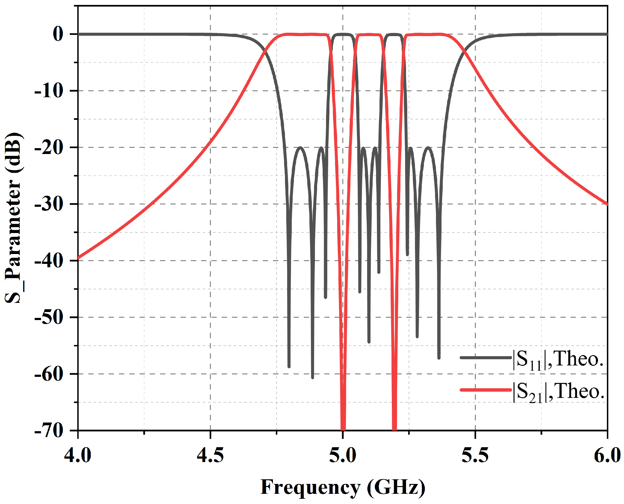
| Filter I | 3/3/3 | 4.81/5.08/5.35 | 4.48/1.84/4.71 | 1.41/2.64/1.39 | >20 dB | 52.41/67.56 | 1.18 × 0.58 |
| [23] | 2/2/2/2 | 11.63/12.47/ | 1.71/1.68/ | 0.89/1.27/ | >15 | >25 | 1.47 × 1.06 |
| 13.51/14.35 | 1.38/1.22 | 1.45/1.36 | |||||
| [29] | 2/2/2/2 | 0.95/1.26/ | 6.7/5.4/ | 2.18/2.09/ | >10 | >25 | 0.5 × 0.5 |
| 1.89/2.29 | 12/15.3 | 1.40/0.93 | |||||
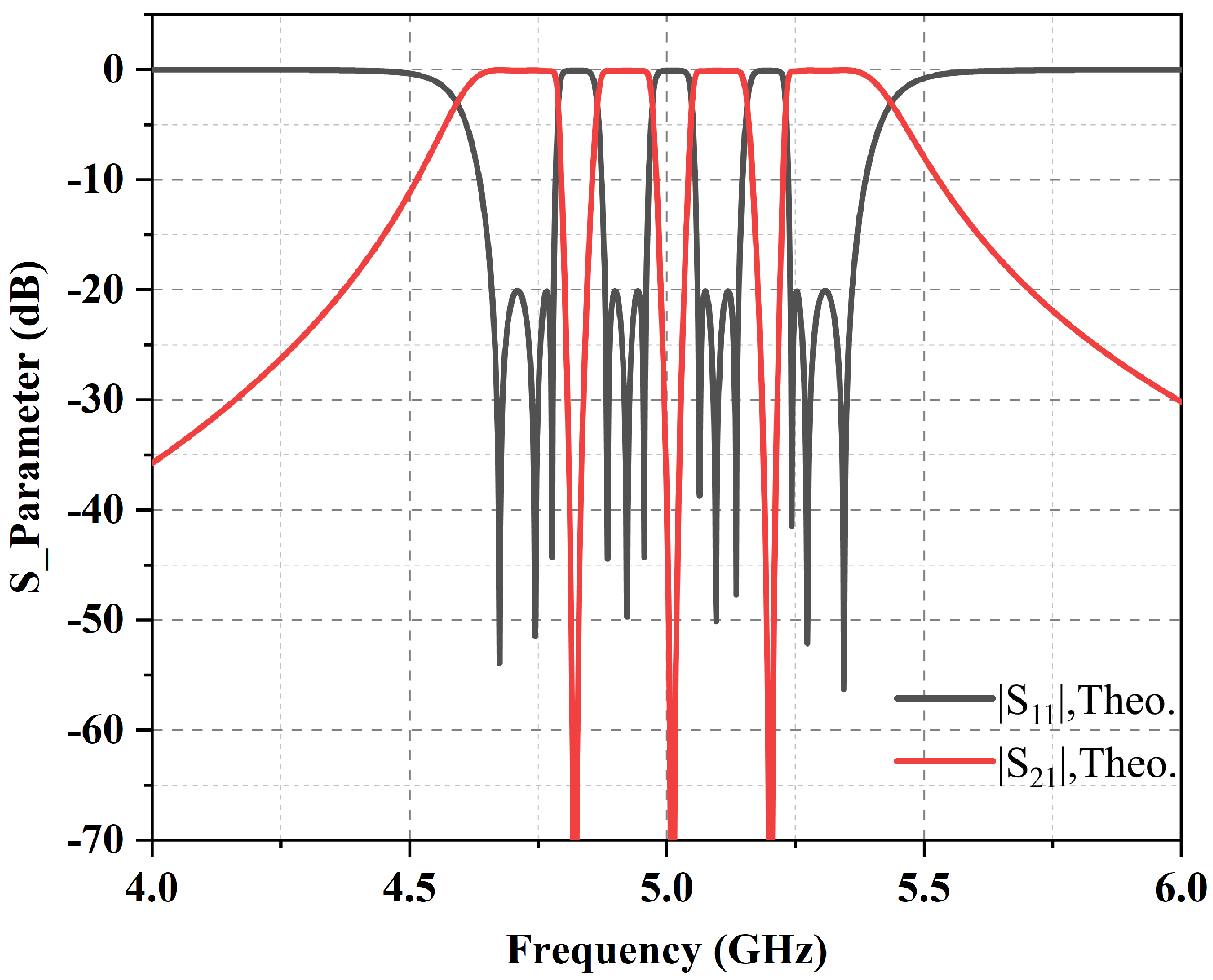
| Filter II | 3/3/3/3 | 4.67/4.91/ | 3.63/1.91/ | 1.64/2.66/ | >18 | 55.06/46.29/ 40.26 | 1.18 × 0.61 |
| 5.09/5.34 | 1.61/3.91 | 2.96/1.87 |
Disclaimer/Publisher’s Note: The statements, opinions and data contained in all publications are solely those of the individual author(s) and contributor(s) and not of MDPI and/or the editor(s). MDPI and/or the editor(s) disclaim responsibility for any injury to people or property resulting from any ideas, methods, instructions or products referred to in the content. |
© 2024 by the authors. Licensee MDPI, Basel, Switzerland. This article is an open access article distributed under the terms and conditions of the Creative Commons Attribution (CC BY) license (https://creativecommons.org/licenses/by/4.0/).
Share and Cite
Zhan, Y.; Wu, Y.; Ma, K.; Yeo, K.S. Miniaturized Multiband Substrate-Integrated Waveguide Bandpass Filters with Multi-Layer Configuration and High In-Band Isolation. Electronics 2024, 13, 3834. https://doi.org/10.3390/electronics13193834
Zhan Y, Wu Y, Ma K, Yeo KS. Miniaturized Multiband Substrate-Integrated Waveguide Bandpass Filters with Multi-Layer Configuration and High In-Band Isolation. Electronics. 2024; 13(19):3834. https://doi.org/10.3390/electronics13193834
Chicago/Turabian StyleZhan, Yu, Yi Wu, Kaixue Ma, and Kiat Seng Yeo. 2024. "Miniaturized Multiband Substrate-Integrated Waveguide Bandpass Filters with Multi-Layer Configuration and High In-Band Isolation" Electronics 13, no. 19: 3834. https://doi.org/10.3390/electronics13193834