Article

A Unified-Mode Analysis Method for Symmetric Networks and Its Application to Balun Design

1
Ministerial Key Laboratory of JGMT, Nanjing University of Science and Technology, Nanjing 210094, China
2
Huaian Key Laboratory of Millimeter-Wave Communication Technology, Huaiyin Normal University, Huai’an 223300, China
3
Yangtze Delta Region Academy of Beijing Institute of Technology, Jiaxing 314019, China
*
Author to whom correspondence should be addressed.
Electronics 2024, 13(19), 3925; https://doi.org/10.3390/electronics13193925
Submission received: 14 August 2024 / Revised: 27 September 2024 / Accepted: 1 October 2024 / Published: 4 October 2024

Abstract

:
A unified-mode analysis method for modeling symmetric networks is proposed in this paper. Adjusting to the characteristics of Marchand balun circuits, a unified-mode circuit model is constructed by introducing virtual impedance. The tenable condition of a Marchand balun with connecting segments is then derived. The parameter constraint of Marchand balun’s input matching is given in a quarter-saddle diagram. Simulated results under different parameter conditions verify the validity of the derived formulas. Based on the derived formulas, the traditional isolation circuit and impedance matching circuit are merged with a Marchand balun to achieve matching for all ports and full-frequency isolation between output ports. A microstrip balun with input and output impedance values of 50 Ω, operating at 1.5 GHz, is simulated, fabricated, and measured. The simulated and measured results of the microstrip balun are in good agreement. When the core parameters remain unchanged, an impedance transformer is inserted in front of the input port of the balun to realize a balun with a topology characterized by flexible impedance transformation. A balun with an input impedance of 35 Ω and different output impedances of 50 Ω and 75 Ω is simulated and fabricated to verify the design concept. Measured results show that an amplitude balance of less than 0.4 dB and a phase balance of less than 3° for a fractional bandwidth of 50%. It should be mentioned that all design equations are closed-form and can be readily employed to design symmetric networks.

1. Introduction

A balun is an indispensable component in circuits and systems involving balanced and unbalanced signals, and baluns are widely applied in balun power division filters [1], low-noise power amplifiers [2,3], balanced mixers [4], frequency multipliers [5], and dipole antenna feeds [6,7]. Depending on the operating frequency and applications, various technologies can be exploited to implement baluns, such as low-temperature cofired ceramic technology [8], CMOS technology [9], active devices [10], lumped elements [11,12,13], transmission lines [14,15,16,17,18,19,20,21,22,23,24], and others [25,26,27,28,29]. The Marchand balun design, named after its inventor [14], is the most popular balun configuration in microwave frequencies by virtue of its good amplitude and phase balance, wide bandwidth, and compact size.
In general, a Marchand balun consists of two quarter-wavelength coupled-line sections in cascade, with the terminations being either open- or short-circuit. Symmetric networks [30,31,32] are usually analyzed by the well-known even–odd-mode excitation method [33], which was proposed by Reed and Wheeler in 1965. For instance, in [21], even–odd-mode half circuits were used in the analysis and optimization of a Marchand balun. In [15], the constraint relation between the impedance-transforming ratio and the coupling factor was derived, and the addition of a resistive network between the balun outputs was proposed to achieve balun output matching and isolation. In [8], a planar balun using aperture-coupled microstrip-to-SIW transition was designed. This did not require the tight coupling employed in most Marchand baluns. In [16], the impact of connecting segments on the balun performance was analyzed. In [23], a new kind of half-wavelength uniform-impedance structure was proposed and used to design a filtering balun with high isolation.
It is noted that the even-mode formulation procedure is repeated for odd-mode circuit in the analysis of symmetric networks, thus increasing the analytical burden. Furthermore, the method cannot directly reveal the evolution from the electric wall to the magnetic wall. A unified-mode analysis method may provide a feasible remedy to the mentioned shortcomings. In the design of coupled-line baluns, there are a lot of published papers dealing with even- and odd-mode analysis. Almost all baluns are designed in such a way as to improve their performances by changing the coupling factor. However, the coupling coefficient cannot fully reflect the external characteristics of the coupled lines [32]. Because of this, the coupling factor may be discarded, which makes the design easier, more flexible, and more transparent to the structural parameters.
In this paper, a new method of analyzing symmetric microwave networks, i.e., a unified-mode analysis method (UMAM), which is different from the traditional even–odd-mode analysis method, is proposed and applied to the analysis and design of Marchand baluns. First, the condition for the establishment of a Marchand balun with connecting segments is obtained, and the design equations without the use of coupling coefficient is then derived in an ideal structure. After that, the parameters of the Marchand balun are simulated by changing the variables in the equations. Third, based on the above, a balun with all-port matching and full-frequency high isolation between balanced ports is proposed. The proposed balun is formed of a Marchand balun, two impedance transformer sections in the balance ports, one half-wavelength phase inverter, and two resistors. Furthermore, a new class of flexible impedance transformation balun with the same advantages is presented. The balun is created by inserting an impedance converter at the input port and keeping its key parameters unchanged. All proposed baluns are simulated, fabricated, and measured. Their good performances, including all-port matching, full-frequency high isolation, and flexible impedance transformation, have validated our proposed design equations.

2. Unified Mode Analysis

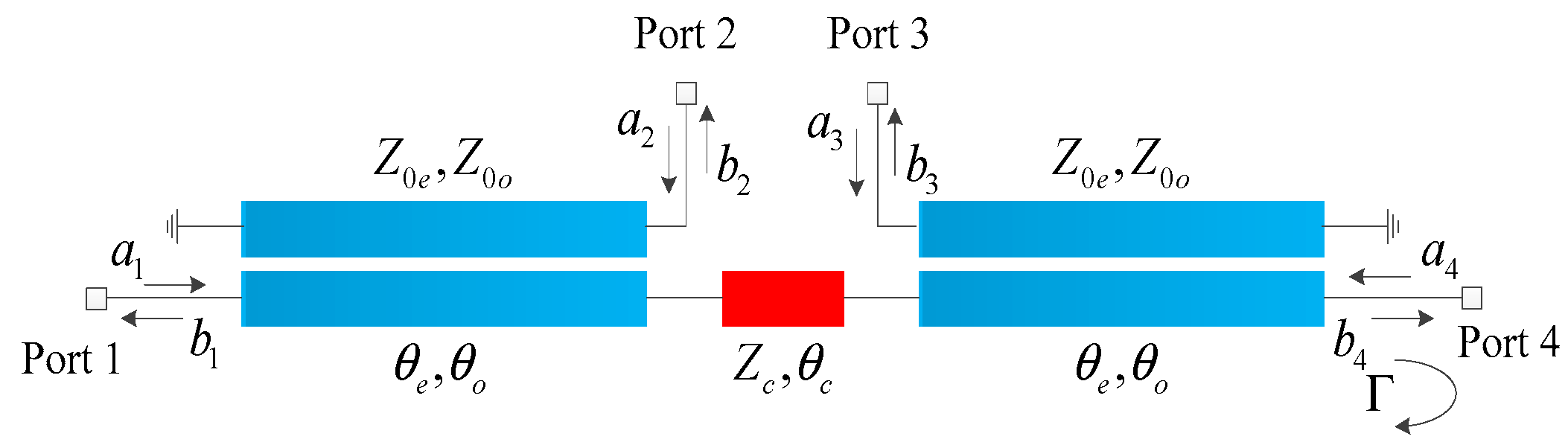
The Marchand balun structure, depicted in Figure 1, is a symmetric four-port network consisting of two sections of coupled transmission lines, a connecting segment, a pair of balanced output ports (Port 2 and Port 3), an unbalanced input port (Port 1), and a floating port (Port 4). For this 4-port network, its scattering parameters, relating the incident waves to the reflected waves at 4 ports (shown in Figure 1), can be expressed as follows:
b 1 b 2 b 4 b 3 = S 11 4 S 12 4 S 14 4 S 13 4 S 21 4 S 22 4 S 24 4 S 23 4 S 41 4 S 42 4 S 44 4 S 43 4 S 31 4 S 32 4 S 34 4 S 33 4 a 1 a 2 a 4 a 3
where a i and b j represent the incident wave at Port i and the reflected wave at Port j, respectively. Port 2 and Port 3 may be terminated with the same load impedance.
Due to its symmetry, the scattering parameters of this 4-port network can be obtained by the even- and odd-mode excitations.
S 4 P o r t = s 11 e + s 11 o 2 s 21 e + s 21 o 2 s 11 e s 11 o 2 s 21 e s 21 o 2 s 21 e + s 21 o 2 s 22 e + s 22 o 2 s 21 e s 21 o 2 s 22 e s 22 o 2 s 11 e s 11 o 2 s 21 e s 21 o 2 s 11 e + s 11 o 2 s 21 e + s 21 o 2 s 21 e s 21 o 2 s 22 e s 22 o 2 s 21 e + s 21 o 2 s 22 e + s 22 o 2
Equation (2) is the S-matrix of the 4-port Marchand balun, described by the even-mode and odd-mode S-parameters. s i j e is the even-mode S-parameter, while s i j o represents the odd-mode S-parameter. In order to obtain the S-parameters of the 3-port Marchand balun, a boundary condition is imposed at Port 4. A reflection coefficient Γ is then introduced at Port 4, as shown in Figure 1. The relationship between the reflected wave and incident wave at Port 4 is a 4 = Γ b 4 . Using this, the scattering matrix of the 3-port network can be presented as follows:
S = S 11 S 12 S 13 S 21 S 22 S 23 S 31 S 32 S 33 = S 11 4 + S 14 4 S 41 4 1 Γ S 44 4 S 12 4 + S 14 4 S 42 4 1 Γ S 44 4 S 13 4 + S 14 4 S 43 4 1 Γ S 44 4 S 21 4 + S 24 4 S 41 4 1 Γ S 44 4 S 22 4 + S 24 4 S 42 4 1 Γ S 44 4 S 23 4 + S 24 4 S 43 4 1 Γ S 44 4 S 31 4 + S 34 4 S 41 4 1 Γ S 44 4 S 32 4 + S 34 4 S 42 4 1 Γ S 44 4 S 33 4 + S 34 4 S 43 4 1 Γ S 44 4
It is well known that the ideal conditions of a Marchand balun are S 21 = S 31 and S 11 = 0 , which leads to
S 21 4 + S 24 4 S 41 4 1 Γ S 44 4 = S 31 4 + S 34 4 S 41 4 1 Γ S 44 4
S 11 4 + S 14 4 S 41 4 1 Γ S 44 4 = 0
When Port 4 is open [14], this means that Γ = 1 . Substituting (2) into (4) and (5), respectively, yields the expressions of the reflection and transmission coefficients of the even-mode and odd-mode circuits:
s 21 e + s 21 e s 11 e s 11 o 2 s 11 e s 11 o = 0
s 11 e + s 11 o + s 11 e s 11 o 2 2 s 11 e + s 11 o = 0
It can be directly seen from (6) that s 21 e = 0 , which is the well-known condition for a Marchand balun [32]. It is known that s 11 e and s 11 o can be denoted as follows:
s 11 e = Y S Y i n e Y S + Y i n e
s 11 o = Y S Y i n o Y S + Y i n o
where Y S is the terminal admittance of Port 1, and Y i n e and Y i n o are the even-mode and odd-mode input admittances with two output ports (Port 2 and Port 3), terminated with a load admittance Y L 
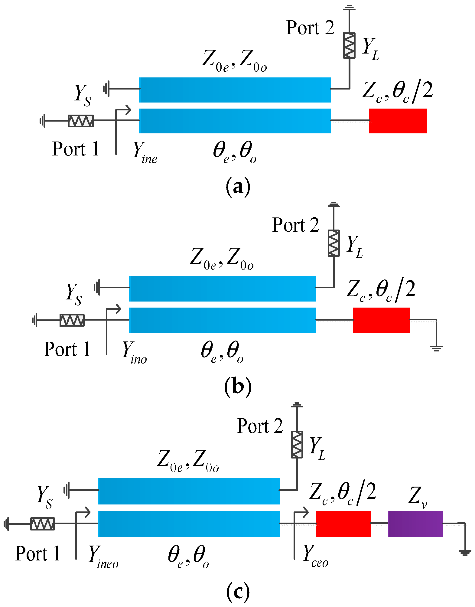
. The Marchand balun’s even-mode and odd-mode circuits are shown in Figure 2a,b. Substituting (8a) and (8b) into (7) obtains the following equation:
1 Y i n e + 1 Y i n o = 2 Y S
For symmetric microwave networks, the analysis method based on even- and odd-mode excitations is the most popular [30,33]. However, two analysis processes are mostly repeated for both modes. In fact, even-mode and odd-mode iterations are the only two limiting cases. For symmetric networks, based on the characteristics of their even–odd-mode circuits, a unified-mode analysis method is proposed here. The idea of the unified-mode analysis is to connect a grounding virtual impedance Z v to the center of symmetric microwave networks. When an odd mode is excited, Z v is zero; for an even-mode excitation, Z v is infinite. Because the odd and even modes are not distinguished, the analysis process is reduced by half. Figure 2c demonstrates the unified-mode model of a Marchand balun, and its admittance matrix for the port voltages and currents is as follows:
I 1 I 2 = M 1 M 4 2 M 1 + Y c e o M 3 M 2 M 4 M 1 + Y c e o M 3 M 2 M 4 M 1 + Y c e o M 1 M 2 2 M 1 + Y c e o V 1 V 2
where Y c e o is the unified-mode admittance, as shown Figure 2c. M 1 , M 2 , M 3 , and M 4 are expressed as follows:
M 1 = j 2 ( Y 0 e + Y 0 o ) cot θ
M 2 = j 2 ( Y 0 e Y 0 o ) cot θ
M 3 = j 2 ( Y 0 e Y 0 o ) csc θ
M 4 = j 2 ( Y 0 e + Y 0 o ) csc θ
Y 0 e and Y 0 o are even- and odd-mode characteristic admittances of the coupled transmission line, respectively. θ is the corresponding electrical length. When the balanced ports are terminated with a load of Y L , the input admittance shown in Figure 2c is expressed as follows:
Y i n e o = M 1 + M 3 M 2 M 4 M 3 M 1 + Y c e o M 1 + Y L M 1 + Y c e o M 2 2 + M 4 M 2 M 3 M 4 M 1 + Y L M 1 + Y L M 1 + Y c e o M 2 2
For the unified-mode circuit shown in Figure 2c, Y c e o is given as follows:
Y c e o = 1 Z c Z c + j Z v tan θ c / 2 Z v + j Z c tan θ c / 2
The corresponding even- and odd-mode admittances, i.e., Y c e and Y c o , are shown to be
Y c e = lim Z v 1 Z c Z c + j Z v tan θ c / 2 Z v + j Z c tan θ c / 2 = j tan θ c / 2 Z c
Y c o = lim Z v 0 1 Z c Z c + j Z v tan θ c / 2 Z v + j Z c tan θ c / 2 = 1 j Z c tan θ c / 2
where Z c is the characteristic impedance of the connecting segment, and θ c is its corresponding electrical length. Substituting M 1 , M 2 , M 3 , and M 4 in (11), and (13) into (12) yields
Y i n e o = ( Y 0 e Y 0 o ) 2 4 Y L + ( Y 0 e + Y 0 o ) 2 4 Y c e o
We can then substitute (13) and (14) into (16) to obtain
Y i n e = ( Y 0 e Y 0 o ) 2 4 Y L + ( Y 0 e + Y 0 o ) 2 4 Y c e
Y i n o = ( Y 0 e Y 0 o ) 2 4 Y L + ( Y 0 e + Y 0 o ) 2 4 Y c o
After that, substituting (17) and (18) back into (9) yields
Z S = 2 Y L Y c e Y c e ( Y 0 e Y 0 o ) 2 + Y L ( Y 0 e + Y 0 o ) 2 + 2 Y L Y c o Y c o ( Y 0 e Y 0 o ) 2 + Y L ( Y 0 e + Y 0 o ) 2
This formula is not only the input port matching condition at the center frequency, but also the condition for the establishment of a Marchand balun with connecting segments.
When the output ports are naturally separated, i.e., θ c approaches 0 degree, (19) can be simplified as
lim θ c 0 Z S = 2 Y L ( Y 0 e Y 0 o ) 2
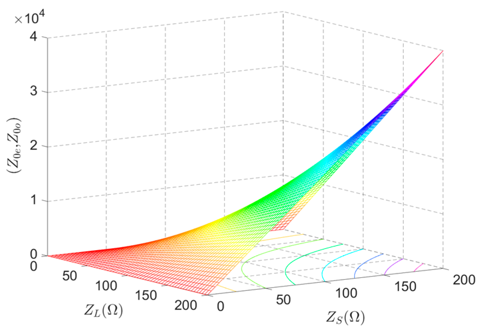
Equation (20) reveals the quantitative relationship between the unbalanced input port impedance ( Z S ), the balanced output port impedance ( Z L ), and even–odd-mode impedances of the coupled transmission lines ( Z 0 e , Z 0 o ). In addition, the quantitative relation is plotted and shown in Figure 3, which is a quarter-saddle diagram for designing a Marchand balun.
To validate the above theoretical analysis, keeping the input impedance constant, the corresponding output port impedances can be calculated according to (20) by varying the even–odd-mode impedances of the coupled transmission line. For instance, the input port reference impedance Z S is set to 50 Ω. Then, the calculated results for several sets of designs are listed in Table 1. The center frequency is fixed at 1.5 GHz. The simulated results of the Marchand balun are then shown in Figure 4.
To further verify the theoretical analysis, for the given even–odd-mode impedances of a coupled transmission line, i.e., Z 0 e = 42.40 Ω and Z 0 o = 22.95 Ω, there are many sets of data satisfying our requirements (20), and a few of them are listed in Table 2. At the center frequency of 1.5 GHz, the simulated results illustrated in Figure 5 are obtained using the data shown in Table 2.
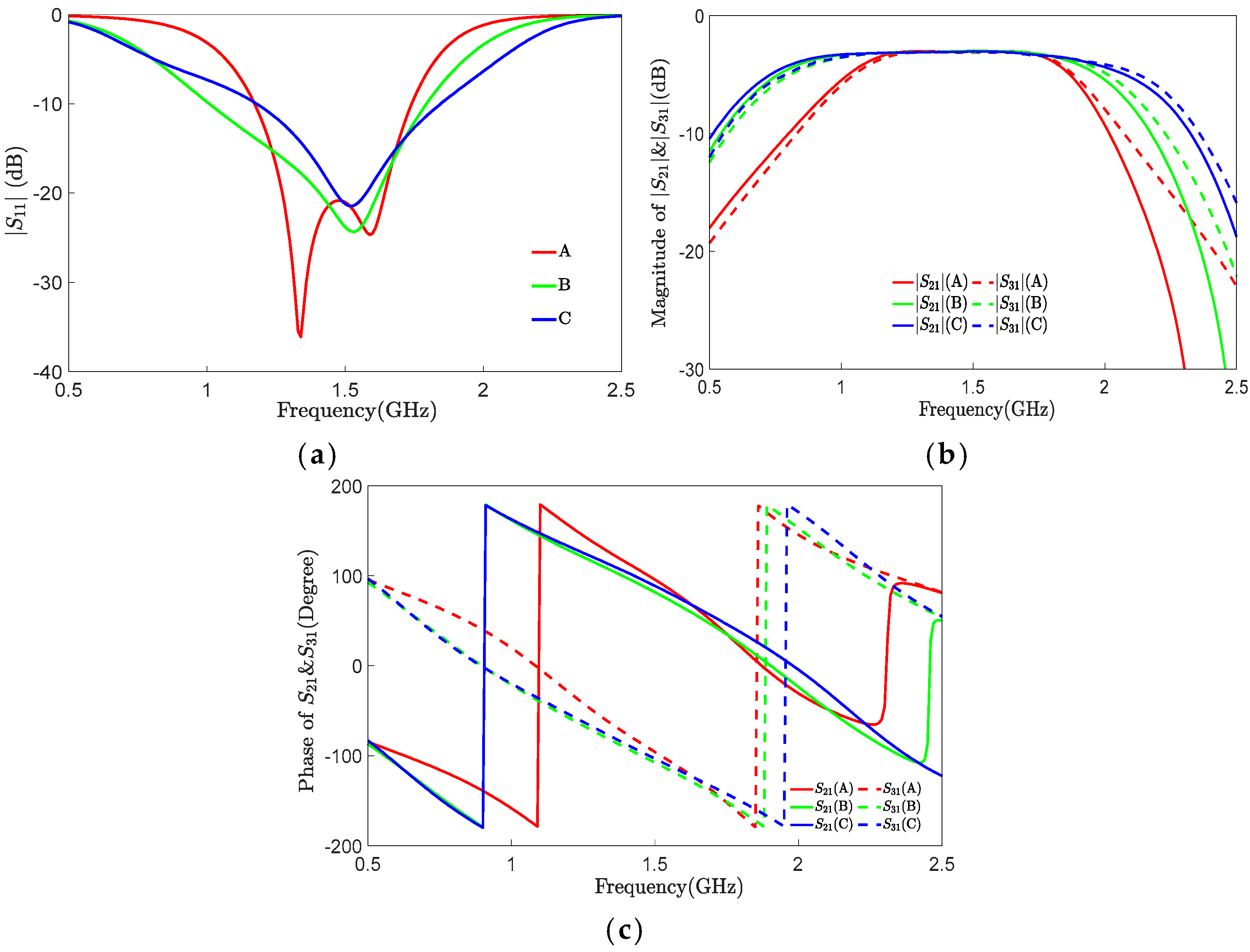
At the center frequency of 1.5 GHz, the input port is exactly matched, as shown in Figure 4a and Figure 5a. Under the same input impedance, Figure 4b,c demonstrate that a larger output impedance leads to a wider bandwidth, higher amplitude balance, and also better phase linearity. When Z 0 e and Z 0 o are kept constant, a larger input impedance results in a wider bandwidth, a smaller amplitude balance, and better output phase linearity, as shown in Figure 5.
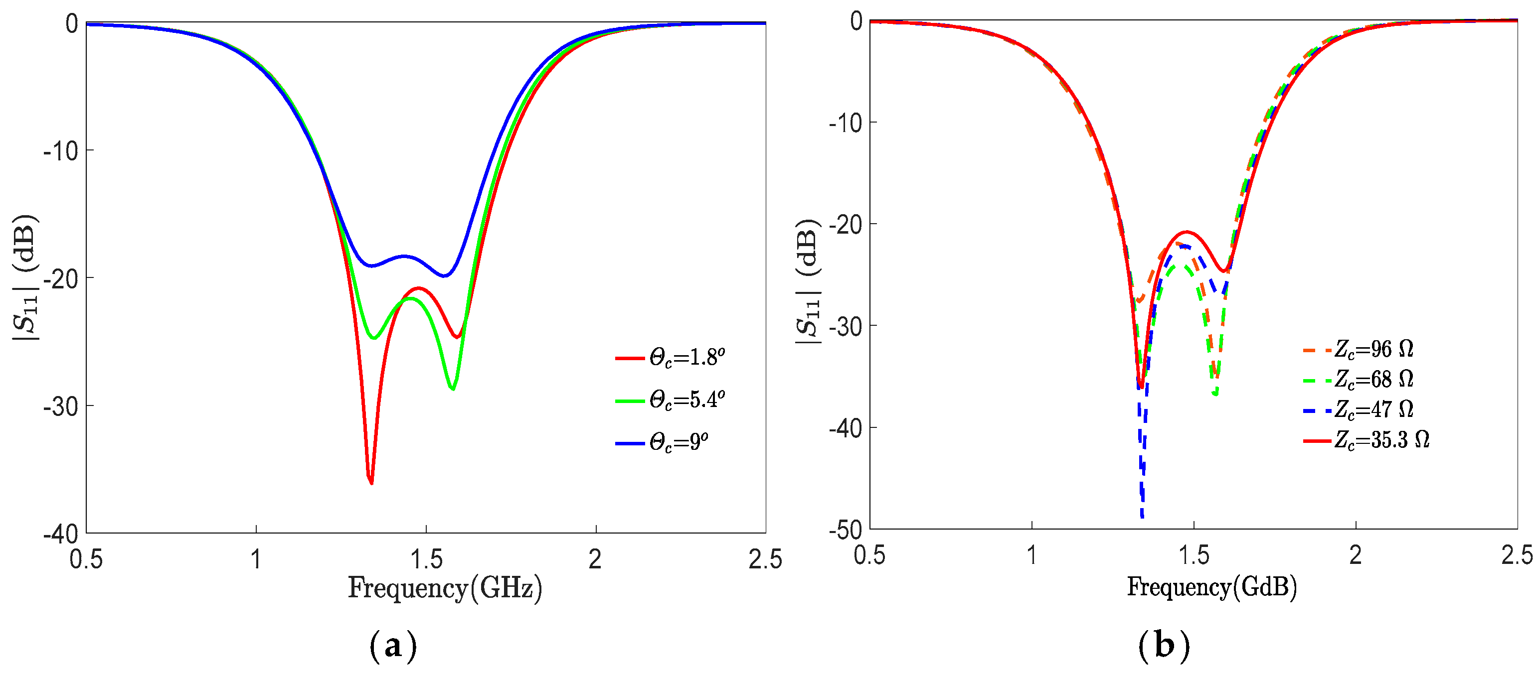
Because of the unavoidable physical separation between balanced ports, it is always necessary to insert additional lines between them. Equation (19) shows that connecting segments have a direct relationship with input port matching. Under the conditions of Z 0 e = 42.40 Ω and Z 0 o = 22.95 Ω, and Z c = 35.33 Ω, Figure 6a reveals the effect of different electrical lengths on input port matching. When θ c = 1.8°, the influence of different characteristic impedances of the connecting section on the input port matching is shown in Figure 6b. It is seen that the change in θ c has a great influence on input port matching.

3. Marchand Balun with Matching and Isolation

It is known that, in principle, a Marchand balun cannot be matched to 50 Ω at all three ports simultaneously [21]. Meanwhile, the even–odd-mode impedances of the coupled line are determined by the line width W, thickness h, the relative permittivity of the dielectric substrate, and the gap between the lines. It is challenging to directly determine the above parameters in a way that can satisfy the given impedance transformation. In [15], for the 50–40 Ω impedance-transformation balun, Lange couplers were designed to achieve the required coupling factor.
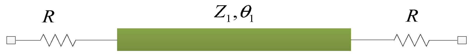
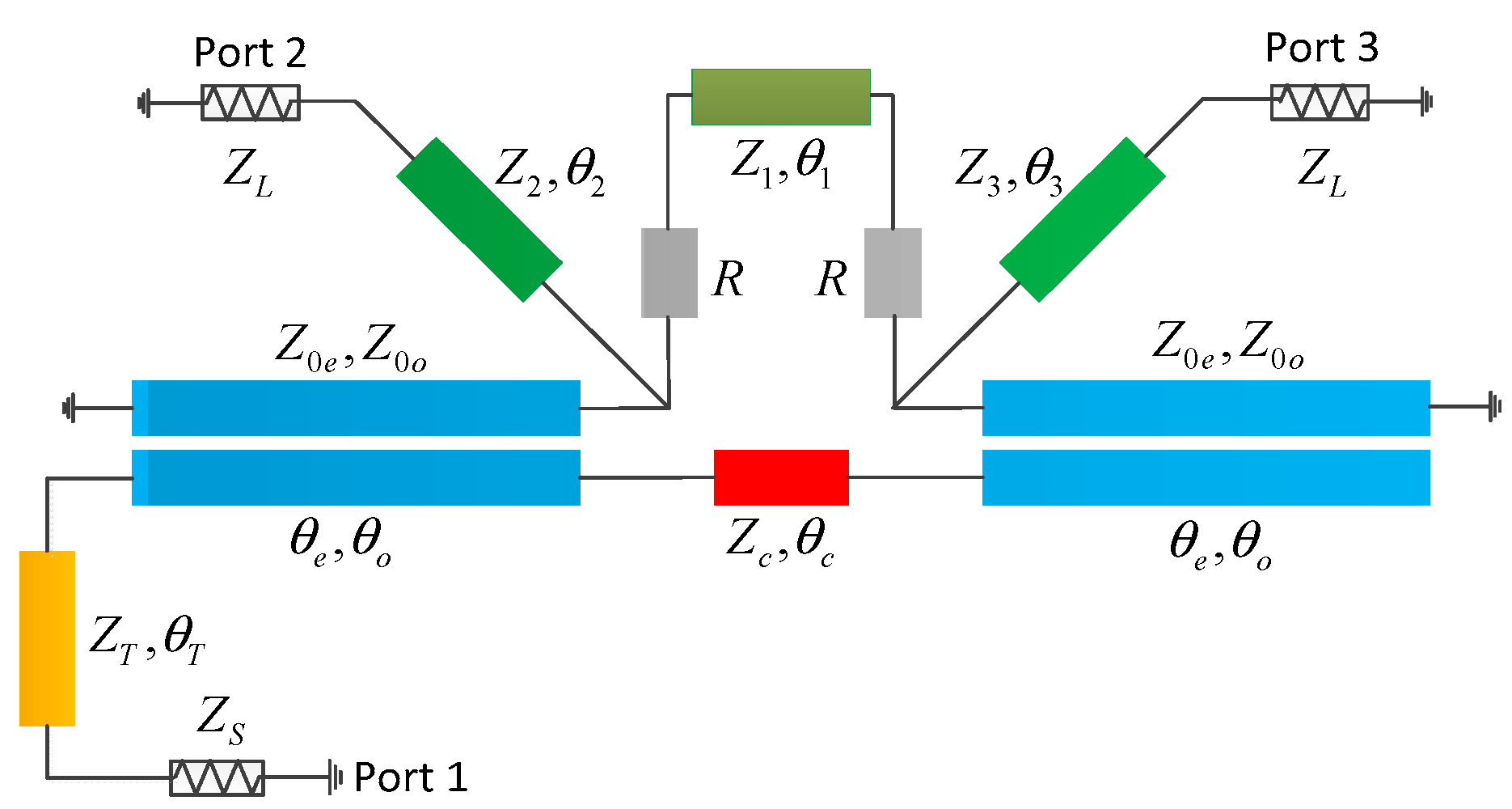
On the other hand, isolation between and the matching of balanced ports are essential in many applications. A network with balanced port isolation and matching is shown in Figure 7, which is constructed by a half-wavelength inverter and two isolation resistors. Its ABCD-matrix at the center frequency can be expressed as
A B C D = 1 2 R 0 1 @ f 0
where R is equal to the impedance of the balanced ports.
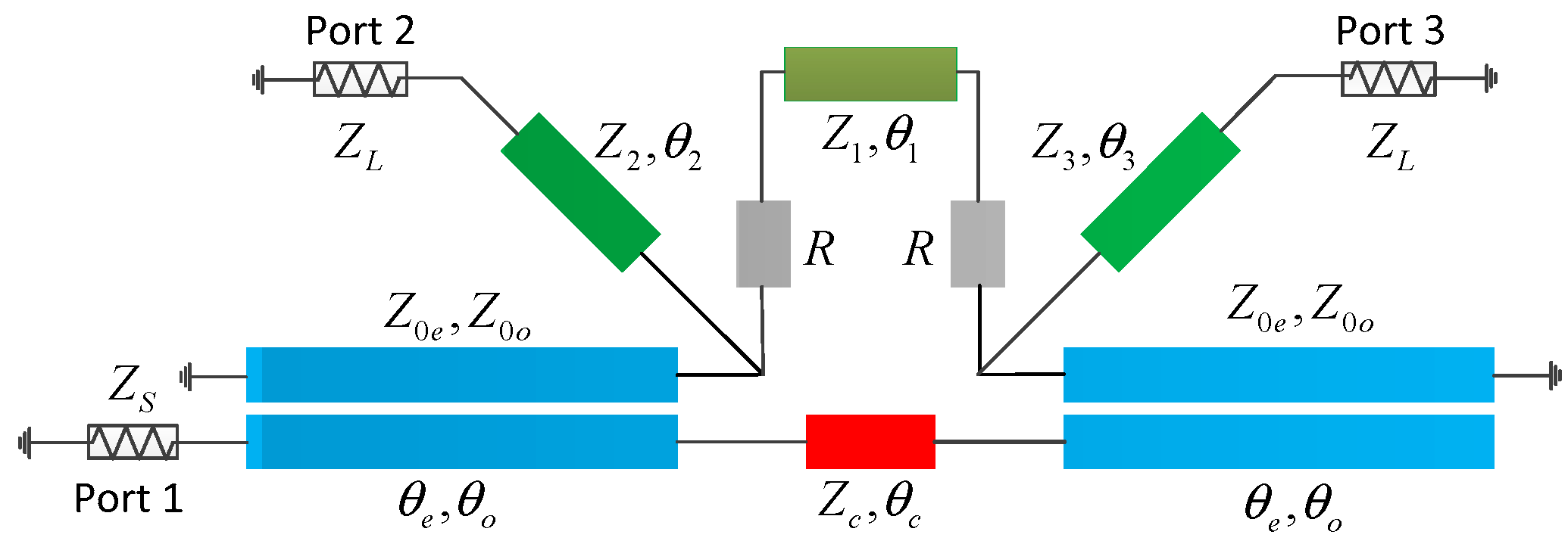
Based on (20) and the isolation circuit structure shown in Figure 7, impedance converter [32] is introduced at the output ports. A balun schematic with all-port matching and full-frequency isolation between balanced ports is proposed and shown in Figure 8.
In order to demonstrate the design approach used to develop a Marchand balun with matching and isolation, a balun with input and output impedance values of 50 Ω and operation at the center frequency of 1.5 GHz is designed. Based on the theoretical analysis in the previous section, the width of the coupled is 1.167 mm, and the gap is g = 0.1 mm. The theoretical values of the impedances Z 2 , Z 3 , and R , indicated in Figure 8, are calculated using the following equations:
Z 2 = Z 3 = 2 Z 0 e Z 0 o Z 0 e Z 0 o
R = 2 Z S Z 0 e Z 0 o Z 0 e Z 0 o 2
The electrical lengths of θ 2 and θ 3 are about π / 4 . All parameters are summarized in Table 3. The simulated results obtained using ANSOFT HFSS are shown in 
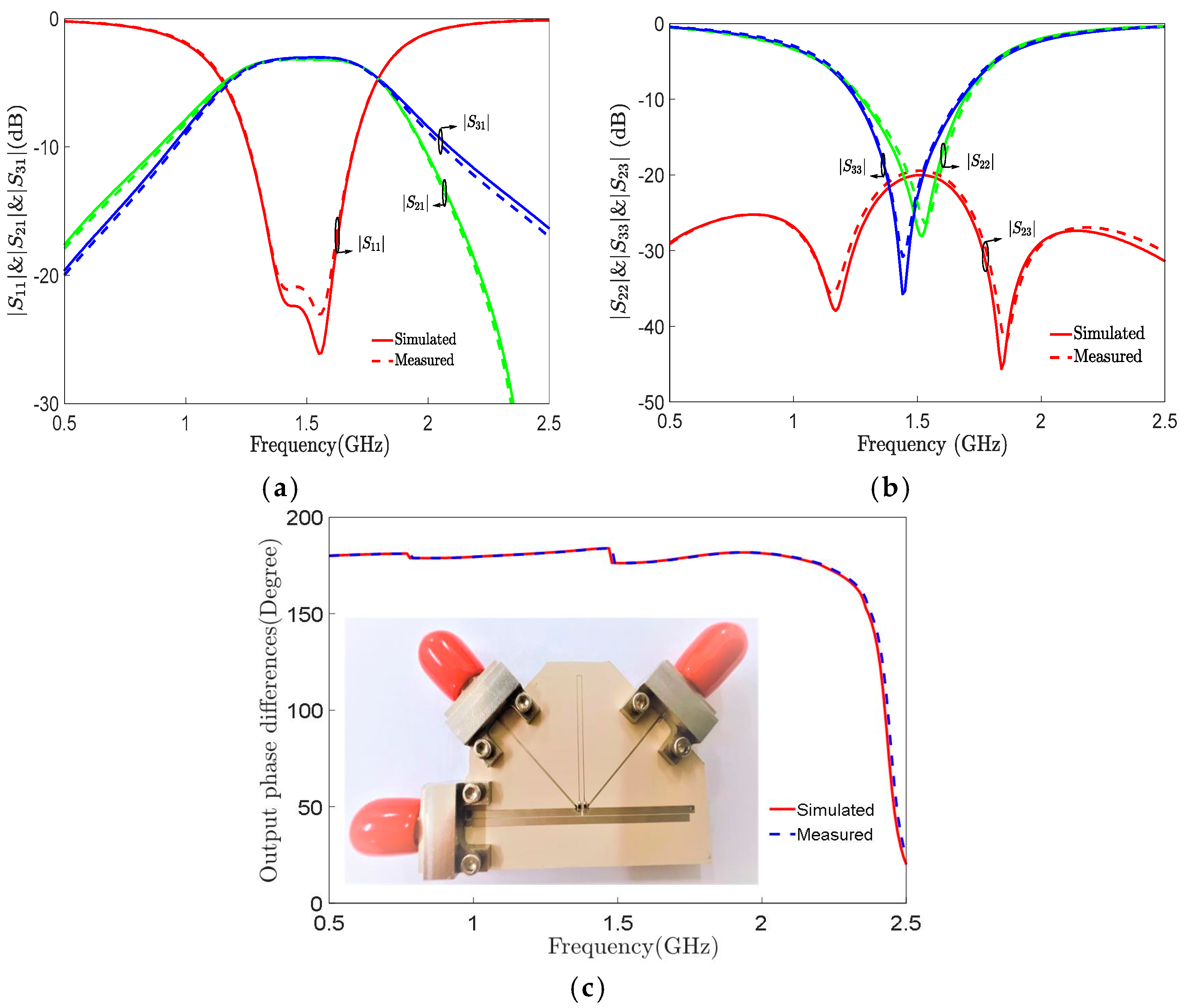
Figure 9. To further prove the design concept, the circuit is realized on a microstrip and fabricated on a substrate (dielectric constant: 9.8, thickness: 0.635 mm). The photo of the fabricated balun is shown in Figure 9c and its scattering parameters are measured using an Agilent N5244A vector network analyzer.
It is seen that the measured results of the fabricated Marchand balun are in excellent agreement with the simulated ones. At the center frequency, all ports are very well matched. The isolation between the output ports is around 20 dB. The magnitude imbalance is less than ±0.39 dB for a fractional bandwidth of 50%, and the phase difference between the balanced ports is within 180 ° ± 2.7 ° . In addition, the layout of the isolation and matching circuits can be optimized to achieve a very compact size.

4. Flexible Impedance Transformation Design

It should be mentioned that previous balun designs have several drawbacks. All Marchand balun designs operate exclusively at a fixed reference port impedance, such as 50 Ω. In practical applications, specifically in end-fire antenna feeding and balanced amplifiers, the impedance of antenna ports or power transistors may be different from 50 Ω. Therefore, the redesign of a balun with a different impedance based on the theoretical analysis presented in this paper is necessary. Based on the theoretical analysis in Section 2 and the sample design in Section 3, and operating under the condition that the balun structure and core parameters designed in Section 3 should remain unchanged, an impedance converter is introduced at the input port. The balun schematic with flexible impedance transformation is shown in Figure 10.
To validate the design concept, two baluns with flexible impedance transformation and operation at a center frequency of 1.5 GHz are designed. Keeping the design structure and core parameter unchanged in Figure 8, according to [32], the theoretical values of the impedance Z T and R , indicated in Figure 10, are calculated by the following equations:
Z T = Z S Z L
R = 2 Z S Z 0 e Z 0 o Z 0 e Z 0 o 2
The electrical length of θ T remains about λ / 4 , which can be finetuned to slightly optimize the balun performance. All the parameters of these baluns are listed in Table 4 and their simulated results are shown in Figure 11 and Figure 12. In addition, these two baluns are also fabricated using the microstrip implementation a substrate (dielectric constant: 9.8, thickness: 0.635 mm). The photographs of the fabricated baluns are also displayed in Figure 11c and Figure 12c. The fabricated baluns are measured with an Agilent N5244A vector network analyzer, and then their measured results are presented in Figure 11 and Figure 12.
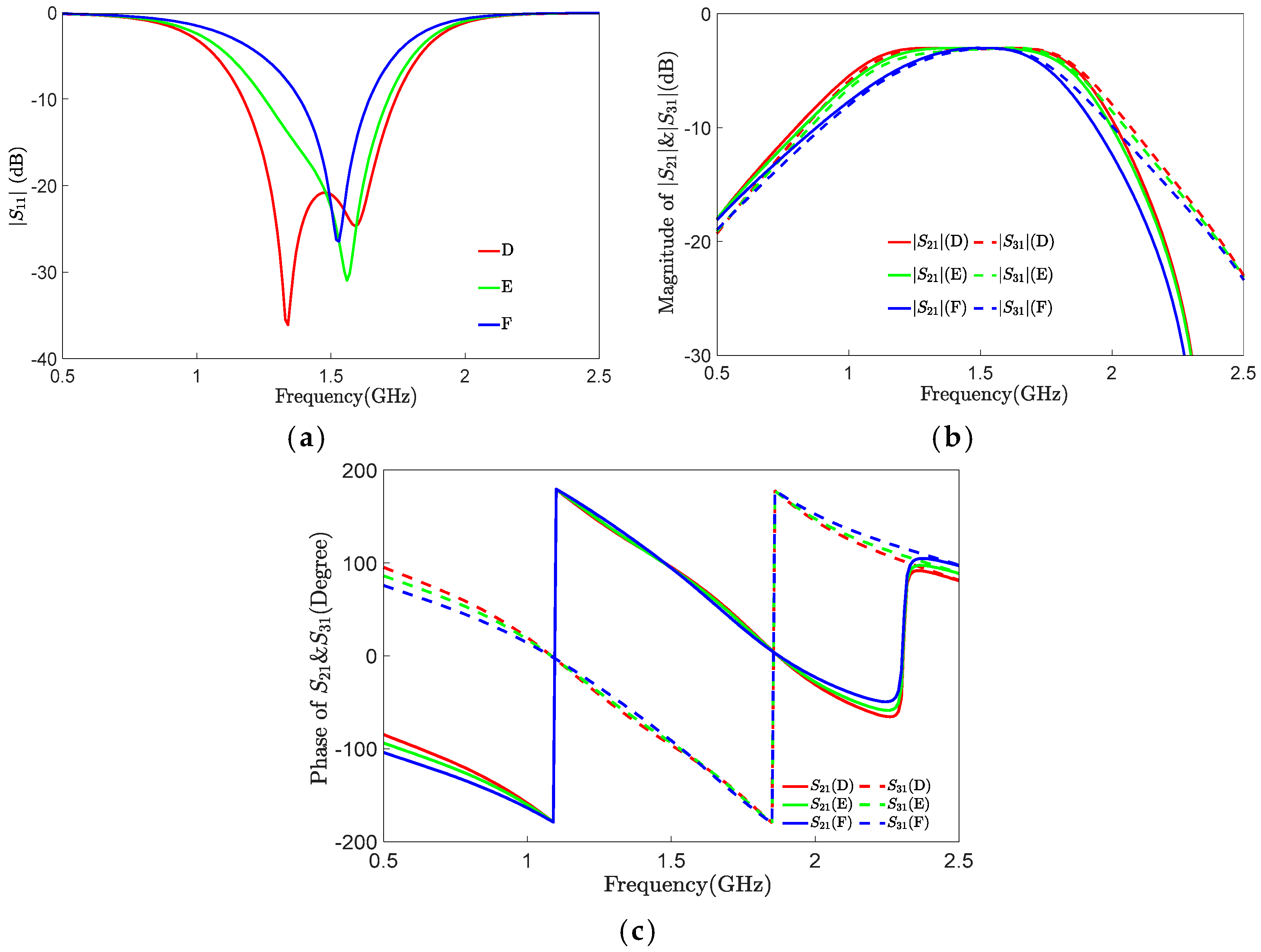
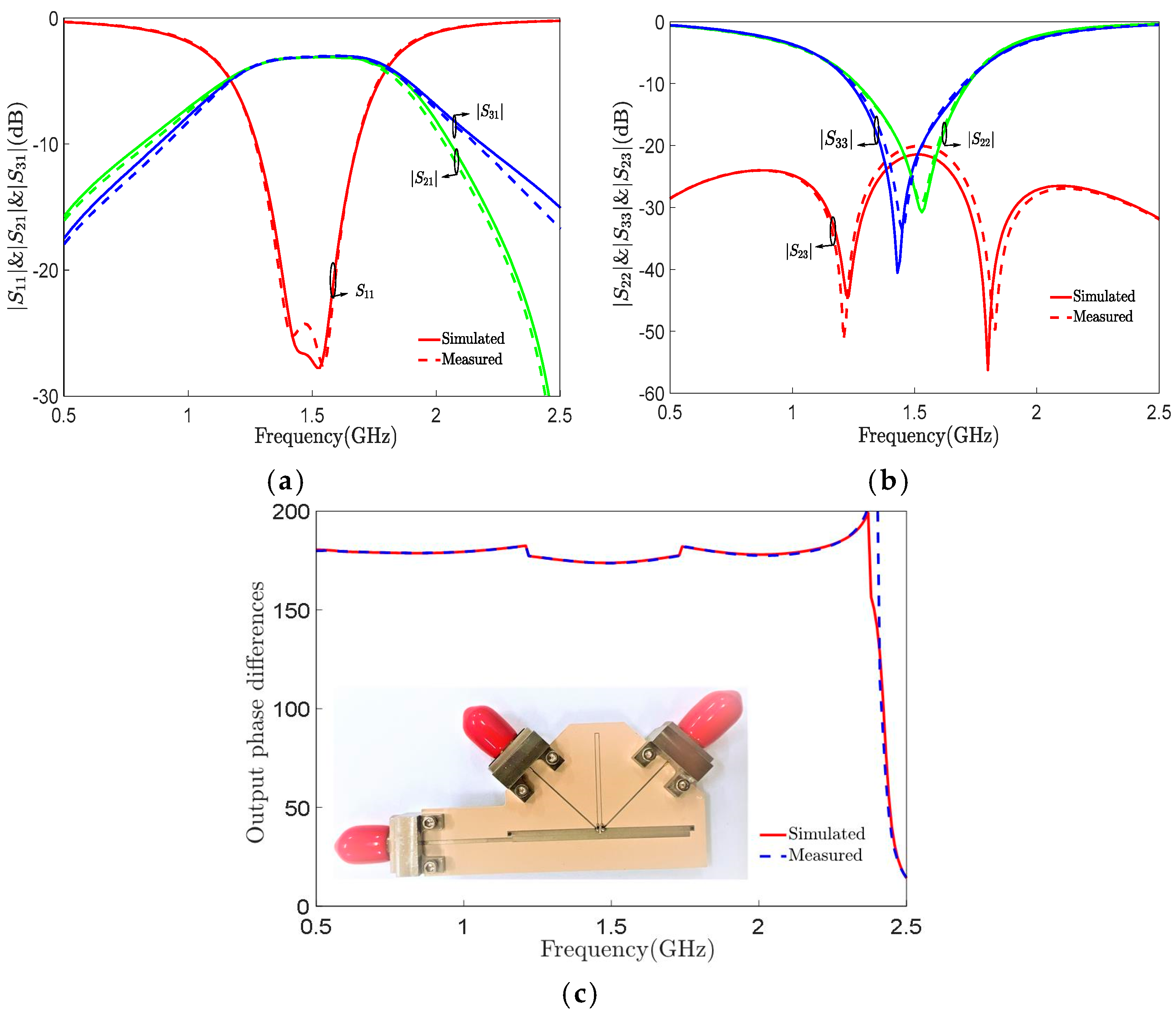
The simulated and measured results of the balun when Z S = 35 Ω and Z L = 50 Ω are shown in Figure 11. It is seen that they are in excellent agreement. The frequency shift in both simulated and measures results is unnoticeable. At the center frequency of 1.5 GHz, the insertion loss is less than 0.4 dB and all ports are very well matched (the measured return loss results are better than 23 dB). In addition, the measured isolation between two output ports is better than 20 dB for all frequencies. The measured magnitude imbalance between the balanced ports is better than ±0.35 dB within the fractional bandwidth of 50%, and the measured phase difference is within 180 ° ± 2.5 ° .
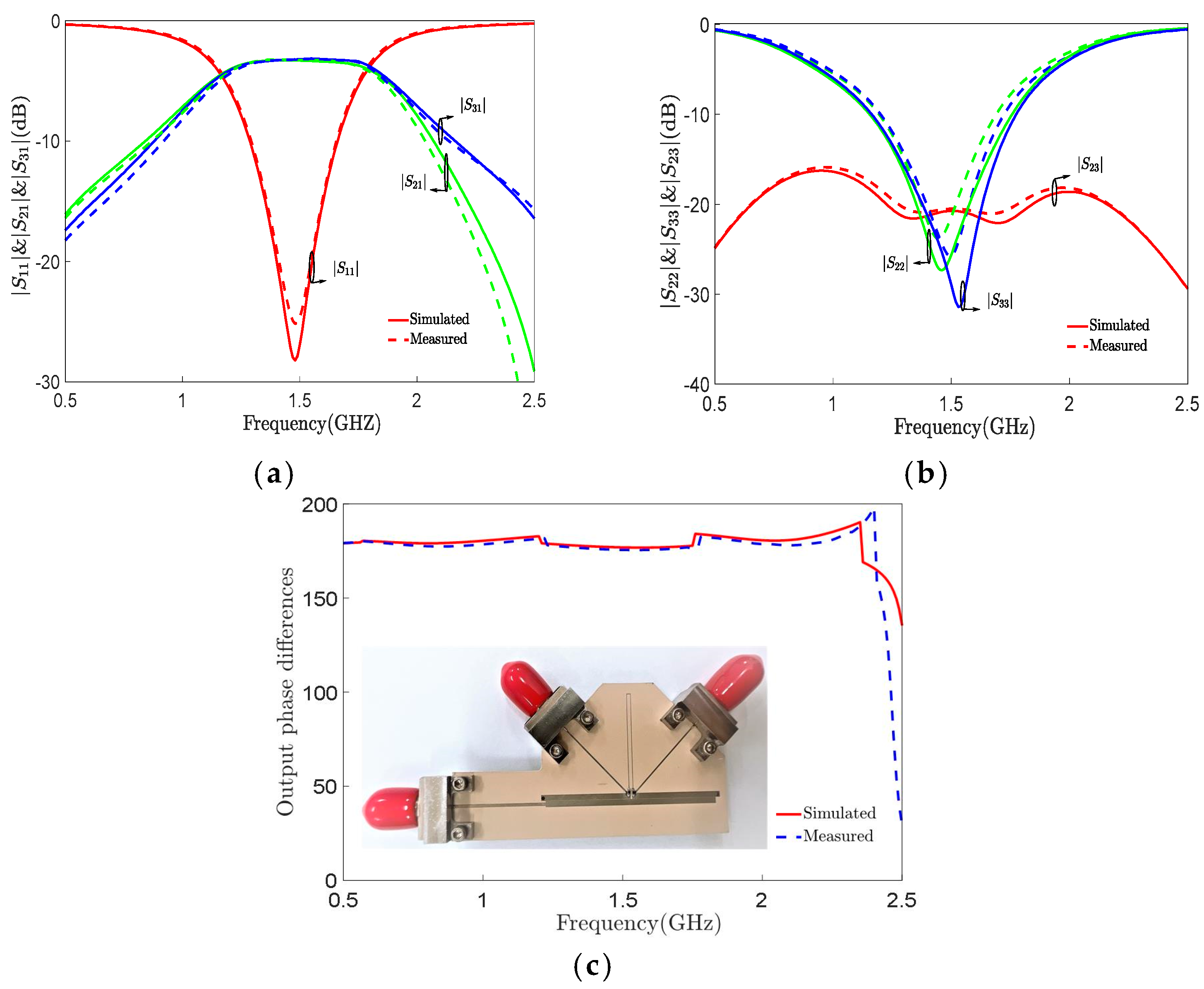
For the other balun, with Z S = 35   Ω and Z L = 75   Ω , the simulated and measured S-parameters are shown in Figure 12. Similar to the previous balun, the measured results of this balun agree very well with the simulated ones. All the ports of the balun with different port impedances are very well matched with a return loss better than 20 dB at the center frequency. The insertion loss is still less than 0.4 dB at 1.5 GHz. The measured isolation between two output ports is better than 16 dB at all frequencies. The measured magnitude imbalance is better than ±0.35 dB within the fraction bandwidth of 50%, and the phase difference between balanced ports is within 180 ° ± 2.2 ° .
From the results presented in Figure 11 and Figure 12, it is seen that baluns with flexible impedance transformation can also be designed to have excellent performance, which proves the validity of the formulated equations. Although excellent agreement between simulated and measured results is observed, there are two obvious differences. One is the center frequency drift directions of | S 22 | and | S 33 |. In Figure 11b, the small drift values of | S 22 | and | S 33 | are to the right and left of the center frequency, while they are reversed in Figure 12b. The frequency shifts are caused by the discrepancy between the odd- and even-mode electrical lengths of the coupled lines and the electrical lengths of the impedance converters. The other one is the isolation between output ports. It is seen that the | | of 35–50 Ω balun is better than that of the balun with 35–75 Ω, which is mainly caused by the resistor R, the impedance matcher, and outport impedance.
To clearly demonstrate the advantages of our proposed baluns, a detailed comparison with other reported baluns is presented in Table 5. Because there are only subtle differences in many parameters between various baluns, such as phase balance, amplitude balance, and return loss, we only compare their implemented functions here. According to the derived formulas, the balun structure has the advantages of all-port matching, full-frequency high isolation between the output ports, flexible impedance transformation, and low insertion loss.

5. Conclusions

In this paper, a unified-mode analysis method for modeling symmetrical networks has been proposed, and the conditions of Marchand balun have then been derived. The validity of the derived formulas has been verified through simulations. Based on the derived formulas, a balun structure with all-port matching, full-frequency isolation between output ports, and flexible impedance transformation has been proposed. Prototypes operating at the center frequency of 1.5 GHz have been simulated and fabricated, and the measured results are in good agreement with the simulated ones. Closed-form design equations can facilitate the design and development of new balun structures. The proposed analysis method can also be applied to calculate the S-parameters and ABCD-parameters of other symmetric networks.

Author Contributions

Conceptualization, L.L., Z.S. and W.W.; Methodology, L.L., Q.L., Z.S. and W.W.; Software, L.L. and Q.L.; Validation, L.L., Z.S. and W.W.; Formal analysis, L.L., Z.S. and W.W. Investigation, L.L., Q.L., Z.S. and W.W.; Resources, L.L., Q.L., and W.W.; Data curation, L.L., Q.L. and Z.S.; Writing—original draft, L.L.; Writing—review & editing, L.L., Z.S. and W.W.; Visualization, L.L.; Supervision, L.L., Q.L., Z.S. and W.W.; Project administration, L.L., Q.L., Z.S. and W.W.; Funding acquisition, W.W. All authors have read and agreed to the published version of the manuscript.

Funding

This work was supported by the Natural Science Research of Jiangsu Higher Education Institutions of China under Contract 22KJA510001 and by the Huaian Natural Science Research Project under Contract No. HABL202106.

Data Availability Statement

No new data were created.

Conflicts of Interest

The authors declare no conflict of interest.

References

  1. Fang, X.; Li, Y.C.; Xue, Q.; Wu, D.-S.; Wong, S.-W. Dual-mode filtering baluns based on hybrid cavity-microstrip structures. IEEE Trans. Microw. Theory Tech. 2020, 68, 1637–1645. [Google Scholar] [CrossRef]
  2. Shin, D.; Lee, K.; Kwon, K. A Blocker-tolerant receiver front end employing dual-band n-path balun-lna for 5g new radio cellular applications. IEEE Trans. Microw. Theory Tech. 2022, 70, 1715–1724. [Google Scholar] [CrossRef]
  3. Martelius, M.; Stadius, K.; Lemberg, J.; Roverato, E.; Nieminen, T.; Antonov, Y.; Anttila, L.; Valkama, M.; Kosunen, M.; Ryynanen, J. A Class-D Tri-Phasing CMOS power amplifier with an extended marchand-balun power combiner. IEEE Trans. Microw. Theory Tech. 2020, 68, 1022–1034. [Google Scholar] [CrossRef]
  4. Wu, Y.-C.; Hwang, Y.-J.; Chiong, C.-C.; Lu, B.-Z.; Wang, H. An innovative joint-injection mixer with broadband if and rf for advanced heterodyne receivers of millimeter-wave astronomy. IEEE Trans. Microw. Theory Tech. 2020, 68, 5408–5422. [Google Scholar] [CrossRef]
  5. Chakraborty, S.; Milner, L.-E.; Zhu, X.; Hall, L.-T.; Sevimli, O.; Heimlich, M.-C. A K-band frequency doubler with 35-dB fundamental rejection based on novel transformer balun in 0.13-µm SiGe technology. IEEE Electron Device Lett. 2016, 37, 1375–1378. [Google Scholar] [CrossRef]
  6. An, W.; Hong, L.; Luo, Y.; Ma, K.; Ma, J.; Huang, X. A Wideband dual-function solar cell dipole antenna for both energy harvesting and wireless communications. IEEE Trans. Antennas Propag. 2021, 69, 544–549. [Google Scholar] [CrossRef]
  7. Yao, W.; Gao, H.; Tian, Y. Compact wideband and variable impedance transformation ratio balun for folded dipole. IEEE Trans. Antennas Propag. 2022, 70, 5935–5940. [Google Scholar] [CrossRef]
  8. Zhang, T.; Li, L.; Zhu, Z.; Cui, T.J. A broadband planar balun using aperture-coupled microstrip-to-siw transition. IEEE Microw. Wirel. Compon. Lett. 2019, 29, 532–534. [Google Scholar] [CrossRef]
  9. Yang, G.; Wang, Z.; Li, Z.; Li, Q.; Liu, F. Balance-compensated asymmetric marchand baluns on silicon for MMICs. IEEE Microw. Wirel. Compon. Lett. 2014, 24, 391–393. [Google Scholar] [CrossRef]
  10. Zimmer, T.; Fregonese, S. Graphene transistor-based active balun architectures. IEEE Trans. Electron Devices 2015, 62, 3079–3083. [Google Scholar] [CrossRef]
  11. Kuylenstierna, D.; Linner, P. Design of broad-band lumped-element baluns with inherent impedance transformation. IEEE Trans. Microw. Theory Tech. 2004, 52, 2739–2745. [Google Scholar] [CrossRef]
  12. Frank, M.; Thorsell, M.; Enoksson, P. Design equations for lumped element balun with inherent complex impedance transformation. IEEE Trans. Microw. Theory Tech. 2017, 65, 5162–5170. [Google Scholar] [CrossRef]
  13. Ye, Y.; Li, L.-Y.; Gu, J.-Z.; Sun, X.-W. A bandwidth improved broadband compact lumped-element balun with tail inductor. IEEE Microw. Wirel. Compon. Lett. 2013, 23, 415–417. [Google Scholar] [CrossRef]
  14. Marchand, N. Transmission line conversion transformers. Electronics 1944, 17, 142–145. [Google Scholar]
  15. Ang, K.S.; Robertson, I. Analysis and design of impedance-transforming planar Marchand baluns. IEEE Trans. Microw. Theory Tech. 2001, 49, 402–406. [Google Scholar] [CrossRef]
  16. Lin, C.-H.; Wu, C.-H.; Zhou, G.-T.; Ma, T.-G. General compensation method for a marchand balun with an arbitrary connecting segment between the balance ports. IEEE Trans. Microw. Theory Tech. 2013, 61, 2821–2830. [Google Scholar] [CrossRef]
  17. Wang, Y.; Lee, J.-C. A miniaturized marchand balun model with short-end and capacitive feeding. IEEE Access 2018, 6, 26653–26659. [Google Scholar] [CrossRef]
  18. Barik, R.K.; Kumar, K.V.P.; Karthikeyan, S.S. Design of a quad-band branch line balun using extended pi-shaped coupled lines. IEEE Microw. Wirel. Compon. Lett. 2016, 26, 771–773. [Google Scholar] [CrossRef]
  19. Barik, R.-K.; Kumar, K.-V.-P.; Karthikeyan, S.-S. A new design procedure for single-layer and two-layer three-line baluns. IEEE Microw. Wirel. Compon. Lett. 1998, 46, 2514–2519. [Google Scholar]
  20. Michaelsen, R.; Johansen, T.; Tamborg, K.; Zhurbenko, V. A Modified marchand balun configuration with tunable phase balance. IEEE Microw. Wirel. Compon. Lett. 2013, 23, 66–68. [Google Scholar] [CrossRef]
  21. Chen, A.C.; Pham, A.-V.; Leoni, R. A novel broadband even-mode matching network for marchand baluns. IEEE Trans. Microw. Theory Tech. 2009, 57, 2973–2980. [Google Scholar] [CrossRef]
  22. Jung, K.; Andrews, M.F.; Hayden, L.A. Rat-race hybrid ring realized in two-layer printed process. IEEE Microw. Wirel. Compon. Lett. 2016, 26, 768–770. [Google Scholar] [CrossRef]
  23. Yan, J.-M.; Zhou, H.-Y.; Cao, L.-Z. A novel filtering balun and improvement of its isolation performance. IEEE Microw. Wirel. Compon. Lett. 2017, 27, 1056–1058. [Google Scholar] [CrossRef]
  24. Ang, K.-S.; Leong, Y.-C. Converting baluns into broad-band impedance-transforming 180º hybrids. IEEE Trans. Microw. Theory Techn. 2002, 50, 1990–1995. [Google Scholar]
  25. Rao, S.G.; Frounchi, M.; Cressler, J.D. Triaxial balun with inherent harmonic reflection for millimeter-wave frequency doublers. IEEE Trans. Microw. Theory Tech. 2021, 69, 2822–2831. [Google Scholar] [CrossRef]
  26. Tseng, C.-H.; Hsiao, Y.-C. A new broadband marchand balun using slot-coupled microstrip lines. IEEE Microw. Wirel. Compon. Lett. 2010, 20, 157–159. [Google Scholar] [CrossRef]
  27. Jia, M.; Zhang, J.; Dong, Y. A compact and broadband balun based on multilayer SIW. IEEE Microw. Wirel. Compon. Lett. 2022, 32, 105–108. [Google Scholar] [CrossRef]
  28. Zhu, F.; Hong, W.; Chen, J.-X.; Wu, K. Ultra-wideband single and dual baluns based on substrate integrated coaxial line technology. IEEE Trans. Microw. Theory Tech. 2012, 60, 3062–3070. [Google Scholar] [CrossRef]
  29. Zhou, J.; Qian, H.J.; Ren, J.; Luo, X. Reconfigurable wideband filtering balun with tunable dual-notched bands using cpw-to-slot transition and varactor-loaded shorted-slot. IEEE Access 2019, 7, 36761–36771. [Google Scholar] [CrossRef]
  30. MartÍn, F.; Zhu, L.; Hong, J.-S.; Medina, F. Balanced Microwave Filters; Wiley: Hoboken, NJ, USA, 2018. [Google Scholar]
  31. Wang, J.; He, S.; You, F.; Shi, W.; Peng, J.; Li, C. Codesign of high-efficiency power amplifier and ring-resonator filter based on a series of continuous modes and even–odd-mode analysis. IEEE Trans. Microw. Theory Tech. 2018, 66, 2867–2878. [Google Scholar] [CrossRef]
  32. Pozar, D.-M. Microwave Engineering, 4th ed.; Wiley: New York, NY, USA, 2011. [Google Scholar]
  33. Reed, J.; Wheeler, G. A Method of analysis of symmetrical four-port networks. IEEE Trans. Microw. Theory Tech. 1956, 4, 246–252. [Google Scholar] [CrossRef]
Figure 1. The configuration of the Marchand balun.
Electronics 13 03925 g001
Figure 2. Half circuits of the Marchand balun: (a) even-mode; (b) odd-mode; (c) unified-mode.
Electronics 13 03925 g002
Figure 3. The quarter-saddle diagram of a Marchand balun.
Electronics 13 03925 g003
Figure 4. Simulated results of a Marchand balun with Z S = 50 Ω: (a) the matching of S 11 ; (b) the magnitude of S 21 and S 31 ; (c) the phase of S 21 and S 31 .
Electronics 13 03925 g004
Figure 5. Simulated results of a Marchand balun with Z 0 e = 42.40 Ω & Z 0 o = 22.95 Ω: (a) the matching of S 11 ; (b) the magnitude of S 21 and S 31 ; (c) the phase of S 21 and S 31 .
Electronics 13 03925 g005
Figure 6. The influence of the connecting segment on the input port matching: (a) Z c = 35.3 Ω and different values of θ c ; (b) θ c = 1.8 ° and different values of Zc.
Electronics 13 03925 g006
Figure 7. Isolation and matching network at the balanced output ports.
Electronics 13 03925 g007
Figure 8. The schematic of the proposed balun with all-port matching and full-frequency isolation between balanced ports.
Electronics 13 03925 g008
Figure 9. Simulated and measured results of 50–50 Ω. (a) Input port S-parameters. (b) Output port S-parameters. (c) Output phase difference and prototype.
Electronics 13 03925 g009
Figure 10. The schematic of the flexible impedance transformation balun.
Electronics 13 03925 g010
Figure 11. Simulated and measured results of a balun with 35–50 Ω. (a) Input port S-parameters. (b) Output port S-parameters. (c) Output phase difference and prototype.
Electronics 13 03925 g011
Figure 12. Simulated and measured results of a balun with 35–75 Ω. (a) Input port S-parameters. (b) Output port S-parameters. (c) Output phase difference and prototype.
Electronics 13 03925 g012
Table 1. Even-odd-mode and output impedances of a Marchand balun with Z S = 50 Ω.
ABC
Z 0 e , Z 0 o ( Ω )42.40, 22.9598.36, 37.74133.61, 46.25
Z L ( Ω )100150200
Table 2. Input and output impedances of a Marchand balun with Z 0 e = 42.40 Ω & Z 0 o = 22.95 Ω.
DEF
Z S Ω 5070100
Z L Ω 1007050
Table 3. Parameters of a Marchand balun with 50–50 Ω.
Characteristic Impedance and Isolation Resistances ( Ω )
Z 0 e , Z 0 o Z c Z 1 Z 2 Z 3 R
42.40, 22.9535.3396.0369.6669.66100
Electrical Length (Degree)
θ e , θ o θ c θ 1 θ 2 θ 3
94.48, 82.731.8180.9390.0690.06
Table 4. Parameters of a Marchand balun with 30–50 Ω and 35–75 Ω.
Z S , Z L
Ω
Characteristic Impedance and Isolation Resistances Ω Electrical Length (Degree)
Z S Z L Z T R θ T
355042.1010091.55
357551.037094.61
Table 5. Comparison with published works.
Ref.f0
(GHz)
MethodologyIL
(dB)
All-Port MatchingAll-Frequency Isolation (dB)
[12]0.9 Geven–odd mode0.8nono
[8]61.75equivalent circuit2.5nono
[27]14.88electric field1.1no<−7.5 dB
[16]1.8voltage wave0.84nono
[17]2.45circuit theory0.62nono
[23]2.42coupling matrix1.5yes<−13 dB
[15]2voltage wave0.5yes<−10 dB
This Work1.5UMAM0.39yes<−19.5 dB
This Work (with FIT)1.5UMAM0.4yes<−20.2 dB (35–50 Ω)
<−15.9 dB (35–75 Ω)
f0: center frequency; FIT: flexible impedance transformation.
Disclaimer/Publisher’s Note: The statements, opinions and data contained in all publications are solely those of the individual author(s) and contributor(s) and not of MDPI and/or the editor(s). MDPI and/or the editor(s) disclaim responsibility for any injury to people or property resulting from any ideas, methods, instructions or products referred to in the content.

