Article

Built-In Self-Test Architecture Enabling Diagnosis for Massive Embedded Memory Banks in Large SoCs

1
Diparimento di Automatica e Informatica (DAUIN), Politecnico di Torino, 10129 Torino, Italy
2
Infineon Technologies, 35131 Padova, Italy
3
Infineon Technologies, 85579 Neubiberg, Germany
*
Authors to whom correspondence should be addressed.
Electronics 2024, 13(2), 303; https://doi.org/10.3390/electronics13020303
Submission received: 28 November 2023 / Revised: 3 January 2024 / Accepted: 6 January 2024 / Published: 10 January 2024

Abstract

:
This paper describes a hardware/software strategy for the effective and efficient management of several distributed Memory Built-In Self-Test (MBIST) units orchestrated by a single CPU to enable the parallel testing of several memory banks. Experimental testing of the implementation on an Infineon chip shows up to a 25% test time reduction compared to traditional strategies, especially in cases for which there are a large number of failures affecting several banks. Additionally, it permits balanced failure collection from different banks in cases for which there are limitations to the storage of failure-related information.

1. Introduction

With constant improvements in terms of clock frequencies and transistor count following Moore’s law, new possibilities arise for designers and programmers for System-on-Chip (SoC) devices. More transistors for a given area allow designers to increase the number of peripherals in their systems without affecting their total area. Developers can then use these peripherals to write increasingly complex memory-greedy programs that require extensive use of the embedded memory (eMemory). As eMemory is a critical part of an SoC, it significantly influences the yield and quality of these devices. For this reason, semiconductor companies place great efforts in their testing and repairing procedures to ensure that each device shipped to the customer complies with the required hardware specifications within the operational conditions [1,2]. This is not a trivial task, as eMemory grows quadratically in capacity with each new generation. Semiconductor manufacturers must then face the escalating challenge of testing increasingly dense and complex memory. It is also essential to minimize the test time of each device as much as possible [3]. Test time is one of the main bottlenecks during the production process and is one of the main costs for manufacturers as they can usually test just a limited number of devices simultaneously. To reduce test time and to tackle the increasing complexity of eMemory, most companies have developed Memory Built-In Self-Test (MBIST) units. They are additional specialized hardware modules that support the Central Processing Unit (CPU) for testing memory, as proposed in [4,5,6]. MBIST units are directly embedded close to the memory circuitry in the SoC and can reduce test times by orders of magnitude by working with full-speed access.
Many approaches found in the literature focus on the organization of the MBISTs, their structures, or the test pattern to apply to the memory. Additionally, other papers deal with MBIST design for multiple memory units. In these cases, either a centralized [4,7] or distributed scheme can be considered [8,9]. To retrieve diagnostic information in the case of a distributed scheme, a possible solution is to check each MBIST one-by-one and perform a linear search to analyze each one’s status register [10].
Even though multiple-memory testing is a well-known topic, if diagnostic information needs to be extracted after a failure notification, there are very few contributions in the state-of-the-art that suggest solutions. Paper [11] describes a potential MBIST-based diagnostic flow for a single memory unit.
The hardware/software scheme proposed in this paper enables improved control of multiple MBISTs operated by the CPU in microcontrollers such as the Infineon AurixTM TC49 used during our tests. Based on the hardware scheme, the system CPU can implement multiple MBIST-access mechanisms while minimizing the system requirements, for example, by using a shared interrupt line to trigger the CPU in case of faults. We specifically designed two approaches: called ’Linear Search’ and ’Binary Search’. In particular, the Binary Search approach is designed to speed up the testing operations and to solve the intrinsic priority issue between multiple MBISTs.
This document is organized as follows. In Section 2, we introduce how eMemory units organized, their testing flows, and the possible architectures of an MBIST. Section 3 is devoted to describing our proposed approach. In Section 4, we present the experimental results and compare different access mechanisms. In Section 5, we draw some conclusions.

2. Background

This section discusses the physical organization of eMemory. Particular attention is dedicated to how the CPU sees eMemory and how the MBIST identifies faults. An overview of the embedded testing flow is given to understand which operations and actors are involved in this process. Afterward, we describe a simple model of MBIST circuitry and clarify its interactions with the rest of the system. Lastly, the focus shifts to how to retrieve the diagnostic information from multiple independent MBISTs.

2.1. Embedded Memory Organization

Embedded storage cells consist of enhanced MOSFET transistors for which the threshold voltage (Vt) is electrically modifiable in a non-volatile manner via charges trapped in an oxide layer or a poly floating gate. Cells can be mass-erased to Low-Vt (LVt or “0”) and bit fine-programmed to High-Vt (HVt or “1”). The fundamental memory elements, bits, are organized in a matrix; rows and columns of bits are named wordlines and bitlines, respectively. A wordline is divided into pages—the smallest programmable or readable unit; to perform a read or a programming operation on any bit, the entire page must be accessed, and updates are page-concurrent but are still slow towards HVt only.
Wordlines are combined into erase segments, called ’logical sectors’, representing the smallest erasable unit. Logical sectors are grouped into physical sectors that, in turn, are combined to form a memory bank. This hierarchy is maintained to obtain different memory sizes, while the number of physical sectors and banks and wordline and bitline dimensions are changed accordingly. This organization is graphically described in Figure 1.

2.2. MBIST Architectures for Diagnosis

Microcontroller eMemory is characterized by highly time-consuming tests. In addition, memory capacity grows quadratically every four years according to Moore’s Law and, similarly, testing times also grow.
The introduction of Memory Built-In Self-Test (MBIST) modules led to a test time reduction for which the magnitude depends on the MBIST structure and the CPU’s and firmware’s ability to access the memory [12,13,14]. Consisting of specialized hardware surrounding the memory, MBIST enables at-speed self-testing without the need for expensive and high-frequency Automated Test Equipment (ATE).
Depending on its complexity, an MBIST’s logic can apply fixed or programmable test flavors and acts as a slave; thus, it must be configured by the ATE or the CPU, respectively, for production tests and online inspections [15,16]. The most straightforward configuration of an MBIST is composed of an Address Generator, a Pattern Generator, a Read/Write Controller, and a Data Output Evaluator [17] as shown in Figure 2:
  • Read/Write Controller is an input to the memory as it decides when its time to write a new test pattern or read it back.
  • Address Generator is also an input to the memory as it decides the address for which the test pattern has to be written to or read from.
  • Pattern Generator decides the pattern to write at a specific address in the memory. It also provides the reference pattern to the Output Evaluator, which can then compare it with the output of the flash memory.
  • Output Evaluator simply compares the output of the memory at a given address with the expected pattern provided by the Pattern Generator. In case of a mismatch, a fault is detected.
MBISTs can access at page granularity and apply patterns and verify the correctness of the read data compared to the expected output. This behavior can be achieved in different ways depending on the MBIST’s complexity and can range from simple ATE-controlled MBISTs to more advanced programmable MBISTs able to interact with the CPU through flags or interrupts.
From a higher point of view, MBISTs with programmable options are usually able to implement many modes of operation [11], including:
  • Count mode: At the end of the memory test, the MBIST makes the total fail count available to the master.
  • Stop-on-fail mode: During the memory test, the MBIST module stops each time a fault is detected and provides the fault’s position and type. After a stop event, the master must resume the verification.
For massive embedded memory composed of multiple banks, the basic structure of an MBIST can be replicated several times. These independent MBIST instances sensibly reduce test time at the cost of a small area overhead. In particular, a distributed MBIST system is better than a centralized one because the test of a fault-free bank is not stopped when a fault occurs in another bank tested by another MBIST instance. The distributed approach gives a significant speed-up during the ramp-up of a technology. An example of a distributed MBIST architecture is illustrated in Figure 3.
Nevertheless, coordinating MBIST instances is not a trivial task. Especially for immature technologies, many banks in the same chip may fail simultaneously. Of course, each unit shows its own fail shape, and several MBISTs must be managed concurrently. In a stop-on-fail scenario, MBIST behavior is resumed only after the current fail coordinate is saved. Meanwhile, many MBISTs can notify of failure and wait to be served. This is especially true for devices with thousands or tens of thousands of faults. In these circumstances, efficiently managing the MBISTs can save up to 26% of test time.

2.3. Linear Search Method

In the case of multiple independent MBISTs integrated into a system [9], it is necessary to access each one of them individually to check their statuses. This is the case for the system represented in Figure 3. The status register is thus the primary communication mechanism used by the MBISTs. After their programming, they only need to write any event (such as “fault found” or “job finished”) to their status register. The CPU can then read the status register of the corresponding MBIST. With the independent MBIST configuration set in the stop-on-fail mode, to understand if a fault has been found in the memory bank, the CPU has to continuously check the MBISTs’ status register in a linear search fashion.
In the simplest scenario in the so-called “linear search” approach, all MBISTs are checked one-by-one, starting from the one with the lowest index as reported in Algorithm 1.
Algorithm 1 Linear Search for N MBISTs
procedure linearSearch(N)
     Start all MBISTs
     while Test not finished do
         for each integer i in N do
            if MBIST[i] found a fault then
                Retrieve fault coordinate
                Restart MBIST[i]
                break
            else
                Continue
            end if
         end for
     end while
end procedure
Linear search is the only possible choice for an architecture that requires individual access to the status register of its MBISTs. A perfect example of this kind of architecture is presented in [10], where the MBISTs are connected to the central controller bus through a multiplexer that selects the desired MBIST on a one-by-one basis. Thus, no parallelization during the MBISTs’ status check is possible using the architecture proposed in [10].
To visualize how the linear search works and its intrinsic issues, Figure 4 and Figure 5 show how this access mechanism works in a possible test scenario with many fails distributed along multiple memory banks. This scenario is an example of what automotive SoC manufacturers may find during the characterization of their devices. Referring to Figure 4 in particular:
  • Banks 0 and 2 represent randomly distributed faults with various shapes.
  • Bank 1 has a faulty bit cell at the junction of the “cross” of failing bit cells. That faulty bit cell appears to work correctly but negatively affects nearby cells.
  • Failures in Bank 3 represent a failing sense amplifier.
The diagram in Figure 5 shows a possible order in which the banks (or better, their MBISTs) requiring CPU attention are served:
  • T0. At the start, each MBIST is in the running phase and is testing the memory in search of faults.
  • T1. The MBIST of Bank 0 is the first to find a fault; it stops the bank test and is waiting for the CPU read. The other MBISTs are still running and are searching for faults.
  • T2. The CPU accesses MBIST 0; MBIST 3 stops and waits while the other MBISTs are still running.
  • T3. The CPU resumes MBIST 0. All the other MBISTs are stopped and are waiting for CPU intervention.
  • T4. The CPU starts analyzing MBIST 1. MBISTs 2 and 3 are stopped and are waiting for the CPU read, while MBIST 0 is again running and is searching for faults.
  • T5. MBIST 0 stops and is waiting for the CPU, MBIST 1 is running. MBISTs 2 and 3 are still waiting for CPU intervention.
  • T6. The CPU starts analyzing MBIST 0. All other MBISTs are stopped and are waiting for CPU attention (MBIST 3 has been waiting since T3).
After T6, if MBIST 0 and MBIST 1 continue to find faults, they will always be served first. With this intrinsic priority, MBISTs 2 and 3 will be served last. This unfair serving of the banks is especially problematic in cases for which there are time or diagnostic memory limitations (i.e., if there is not enough space to store all fault information, faults appearing in Banks 2 and 3 will not be logged).

3. Proposed Approach

The proposed approach considers the usage of CPU firmware supported by an additional hardware structure, as illustrated in Figure 6A). Such ad hoc circuitry controls a status bit value by ORing the status bit spilled from every MBIST. When a fault occurs in any memory, this flag bit raises to value one and triggers the CPU similar to an external interrupt. The processor, left in idle mode, wakes up from idle and interacts with a bank selector register to identify the failing bank following the approach shown in the following paragraphs. This hardware organization is cheap because of CPU reuse to support memory testing and because it demands very few extra gates. For sure, a single flip-flop could be extended to a register. However, it would not fit other constraints, such as the number of interrupt channels, other than for area overhead minimization. A status register without interrupt capabilities would require continuous polling by an always-awake CPU, which would impact device consumption during the test execution.
Therefore, distributed MBISTs supported by the proposed hardware add-on allow the execution of concurrent memory bank tests. Consequently, it sensibly reduces test time with small area and power demands. This paper focuses on getting maximum performances out of this scheme without sacrificing the effectiveness of the collected failure coordinates, especially in cases of simultaneous fails detected on different MBISTs.
Overall, we compare three different methods:
  • A linear search method, which is considered as a baseline for comparison.
  • Two versions of a binary search method: without and with priority shifting.
Among these methods, binary search with priority shifting achieves a better trade-off between test time and the retrieved failure information quality, i.e., overcoming the limits highlighted in Section 2.3 about diagnostic data collection.

3.1. Hardware Architecture for Diagnosis

The hardware design used for our approach enables concurrent access to one or more MBIST status registers by providing the ORed version of all the selected ones in one readout. Considering the case in which all MBISTs are addressed for a status register readout, a raised stop-on-fail flag means that at least one module needs to be served by the CPU.
Figure 6A depicts a simplified model of the proposed hardware organization. The status register bit accessible for readout contains the ORed information of all MBISTs selected through the bank selector. That is an array composed of as many bits as there are MBISTs available. The output of an MBIST is enabled when its corresponding bit in the bank selector is set to one. To understand if at least one MBIST found a fault, the CPU must check the common status register bit through polling or by waiting for an interrupt. Independent of the chosen solution, this organization shows clear advantages in circuit complexity and test time compared with an arrangement wherein each MBIST has its own status register. Reducing the number of needed registers is a major contributor to area savings. For what concerns the test time, as we will see in the following section, this organization allows for clever search algorithms that exploit the common status register bit. Architectures with completely independent MBISTs, such as the one presented in [10], can only resort to the linear search algorithm, which will be used as a reference to evaluate the performance of the proposed algorithms.

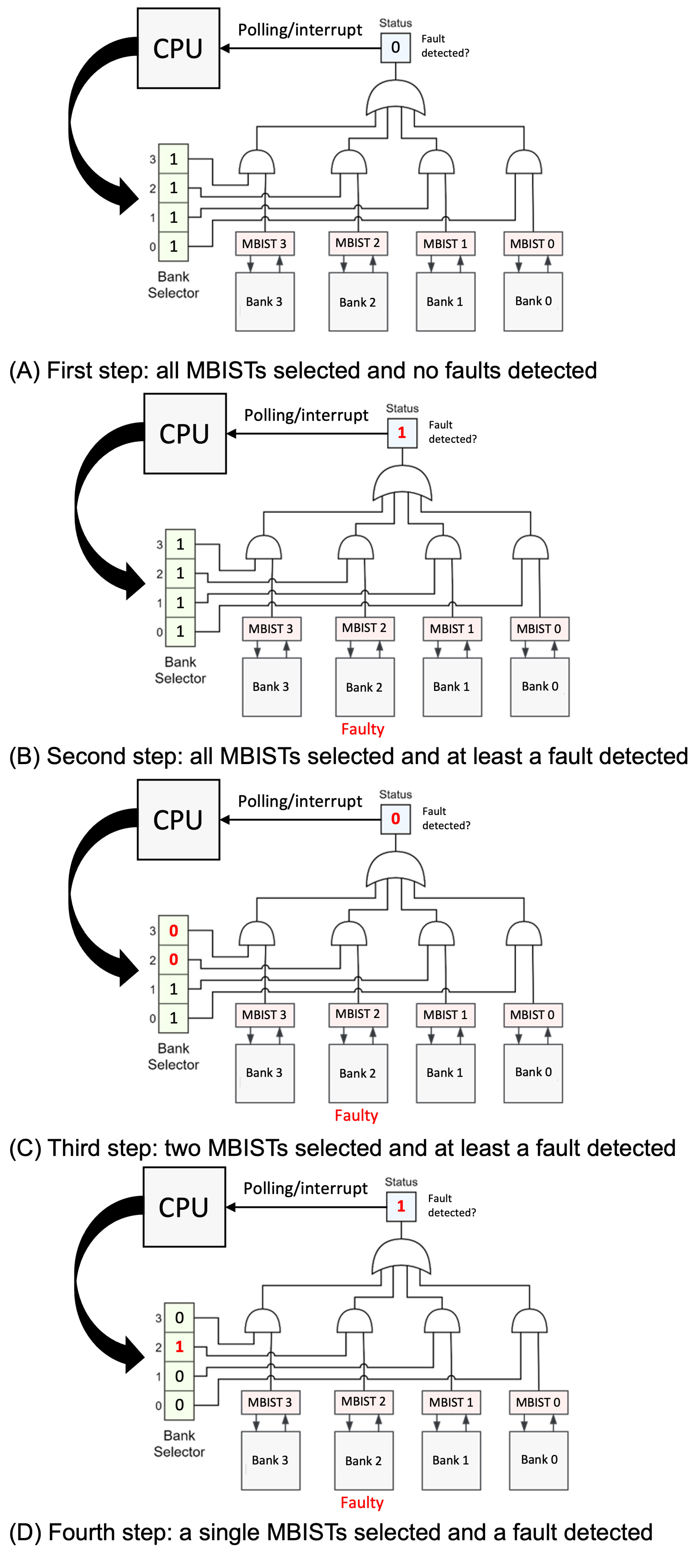
3.2. Binary Search Approaches

The goal of the proposed search algorithm is to overcome the intrinsic problems of linear access that affect the overall test time. Taking advantage of the capability of our proposed schema, it is possible to shorten the test time by relying on a tailored binary search procedure such as the one described in Algorithm 2.
Algorithm 2 Binary search for N MBISTs
procedure BinarySearch(N)
     Start all MBISTs
     Start = 0
     End = N − 1
     Enable all MBIST outputs
     while Test not finished do
         if common status bit is 1 then
            while end − start != 0 do
                middle = (start + end)/2
                Enable output for MBIST[start] to MBIST[middle]
                if common status bit is 1 then
                    end = middle
                    Continue
                else
                    start = middle
                end if
            end while
         end if
     end while
end procedure
In our scenario, the binary search algorithm generates the bitmasks to be loaded into the bank selector.
Figure 6 shows how binary search is applied in the case of four MBISTs by disabling or enabling the outputs of groups of MBISTs. Once a fault has been found by at least one MBIST, the ORed stop-on-fail flag is raised. This flag generates an interrupt that wakes the CPU from idle. At this point, the algorithm generates a bitmask containing “half 0s” and “half 1s”: enabling the ORed flag of MBISTs 0 and 1 (half the MBISTs available). The algorithm will continue analyzing the rightmost half if the flag is high. Otherwise, it will proceed on the leftmost half. The analysis iterates, halving the number of MBISTs to evaluate step-by-step. At the last step, a bitmask containing only one bit set to “1” is applied, and the procedure returns the index of the bank to be served.
With this approach, in case of fault, exactly log2(N) checks are needed to identify the correct MBIST. In case of no faults, one check is enough for all the MBISTs. Anyway, the pure binary search approach still suffers the intrinsic propriety order of access seen in Section 2.3. For example, let us analyze the case in which every bank requests an action from the CPU (Figure 7a): the selected bank to be served will inevitably be the rightmost one. This unintended fixed priority could lead to undesirable starvation of “stopped” MBIST modules. Consider, for example, an event wherein one memory module completely fails and the rest present only one fail on the first page; suppose that the entirely failed memory module has the highest intrinsic priority. All the MBISTs will start concurrently, and they will all stop on the first page. The CPU will serve and repeatedly resume the entirely failed bank, preventing the other MBISTs from stepping over the first failing page and proceeding concurrently.
To overcome this problem, we developed a revised binary search by merging the superior performance of the binary search with the starvation-free capability of round-robin scheduling.
To achieve this priority changeover in the served MBIST, an n-bit rotation to the bank selector generated at every step of the algorithm is applied: n is increased by one each time “binary search with priority shifting” is executed.
Figure 7b analyzes again the case in which multiple MBISTs need to be served by the CPU at the same time: applying a 1-bit right rotation to the bank selector, the priority is shifted from the rightmost module (MBIST0) to the leftmost one (MBIST3).
For manufacturers, it is crucial to have as much information as possible about the failures in their systems. However, in a production environment, a trade-off between the accuracy of the collected information and its costs must be explored; this includes test time and diagnostic memory size.
A common approach when there are memory limits consists of assigning a fixed amount of on-chip memory for storing as much diagnostic information as possible. This constraint limits the number of fault locations that can be stored on-chip during the tests. Without a specific division of the available on-chip memory between the different MBISTs, a manufacturer may lose important insight into of some the memory units under test. For example, in a scenario with a memory bank showing a lot of failures (enough to fill the assigned memory space) and another with a few, if the priority is fixedly given to the MBIST self-testing the memory with more failures, then the fault information from the other one may not be collected. For a producer, this is the worst possible situation; it would be much better to renounce some information about largely failing banks than totally missing indications about a failing memory bank.
Figure 8a–c illustrate the issue. It uses a memory module with four banks as a reference; each bank has its own MBIST.
A
Figure 8a shows all the failures in the memory. Without an on-chip memorization limit, the total test time is the only difference between the three access methods presented in this paper.
B
In Figure 8b, there is a limit to the on-chip memory available to store diagnostic information. Using the linear and binary search approaches, the BIST of Bank 0 is always served first. Bank 1’s BIST is served next and fills the remaining reserved memory space. As can be seen, no information about Banks 2 and 3 reaches the external world as the reserved memory is already saturated when their MBISTs are served.
C
Figure 8c shows the effect of the binary search with priority shifting in case the memory limitation is still in place. The result is a fairer memory representation with partial information from all the memory banks.
Binary search with priority shifting ensures a fair representation of the different banks in the memory. Of course, the trade-off is represented by the partial representation of these banks. Nevertheless, it is essential to notice that it is often possible to extrapolate fault patterns and understand their causes even with partial information.

4. Experimental Results

This section analyzes the behavior of the proposed hardware and software scheme in real-case scenarios. We used a subset of the tests usually executed during the characterization of the SoC. As execution time is the best metric for this kind of test, we analyze the three access mechanisms’ timing behavior. All of them were executed in an InfineonTM SoC with the MBIST organization described by our approach and using polling to check the MBISTs’ common status register. The following experimental results examine three scenarios: a sweep of artificially injected errors, data from real faulty devices, and some special cases. In the following sections, the linear search algorithm is used as a reference for comparison with the basic and priority shifting binary search algorithms. The two binary search methods exploit the architecture proposed in this paper. Such optimized algorithms cannot be implemented in architectures with isolated MBISTs like the one presented in [10]; these architectures can only implement the linear search method.

4.1. Sparse Faults Randomly Distributed

Sparse faults randomly distributed along the memory are one of the common issues with embedded memory. To emulate the sparseness of defective bits that characterizes real devices, 5000 tests were performed under these conditions:
  • Single-bit error (SBE) only: at most, a single bit per page can be faulty;
  • Pseudo-randomly generated addresses: the indexes of faulty pages are calculated in a pseudo-random manner;
  • Number of injected errors is between 0 and 90 k, which roughly corresponds to 0.03% of the bits in the memory.
The faults generated by this random approach are very similar to those obtained during tests performed during the characterization of the sense amplifiers of the DUTs and generate a semi-random distribution of faults along the entire memory.

4.2. Test Time Comparison

In our experiments, it is clear that the test times are directly proportional to the number of injected faults for all three analyzed algorithms in a linear manner. The superiority of the binary-search-based approaches results in a time reduction of roughly 25% compared to the linear search. The standard implementation provides the best performances, leading to a 26.3% test time reduction, while the binary search with priority shifting is limited to 23.9% (the 2.4% overhead is due to the rotation of the bank selector).
Table 1 shows our results with respect to the time overhead of the three methods with increasing fail counts. In this experiment, we injected variable amounts of sparse fails on a single device. As we can see, the binary search approaches have a sensible advantage over the linear one.

4.3. Progress of Bank Verification

To test the evolution of bank verification, we devised an experiment in which we injected pseudo-random SBEs into roughly 0.006% of the memory. This experiment aimed to prove that the linear search and binary search methods prioritize the banks with the lower index. In contrast, the binary search with priority shifting makes all MBISTs proceed in parallel to the greatest extent possible.
The line plots in Figure 9a–c (with the banks’ color legend in Figure 9d) highlight how the intrinsic priority affects the progress of the MBISTs’ memory verification. The x-axis represents the test duration, with 100% being the overall time that the linear search needs. The y-axis measures the ratio of faults found by each MBIST and the total number of errors in the corresponding bank, which is expressed as a percentage. The time reduction of the two binary-search-inspired approaches is over 25%.
This behavior can be easily discerned in Table 2 and Table 3. These tables shows the percentages of faults analyzed by the three access methods in five different banks at 10% and 30% of the test time (with 100% representing the time required for the linear search).
For the 10% test time represented in Table 2, it can easily be seen that the linear search and the binary search have similar behavior:
  • Faults in Banks 0 and 4 start to be analyzed, with Bank 0 receiving the most attention;
  • All faults in the other banks are not analyzed.
By contrast, the binary search with priority shifting shows a “fairer” distribution of the analyzed faults. Bank 0 is still the most analyzed (perhaps because MBIST 0 is the first that the CPU programs and starts). Banks 4, 8, 12, and 14 are all analyzed to a certain degree based on factors such as fault location and, consequently, the detection time for all MBISTs.
For the 30% test time represented in Table 3, again, the priority of lower-indexed banks is clear in linear and binary searches:
  • Faults in Banks 0 and 4 are completely analyzed at 30% test time;
  • Faults in Bank 8 are starting to be analyzed;
  • Banks 12 and 14 are not even reached at this point.
With the binary search with priority shifting, Bank 0 is still the most analyzed, while Banks 4, 8, 12, and 14 are all analyzed up to a certain degree.
Figure 9a–c also show what happens in case of a 24 KB limit for the representation of diagnostic information. The dashed purple lines represent the point at which the 24 KB are saturated in the different scenarios. The saturation happens in different conditions for the three tested algorithms:
  • For the linear and binary search algorithms, the intrinsic priority of the lowest-indexed banks is clear. Banks 0 to 4 are completely represented in both cases. The other banks are analyzed just partially or not analyzed at all, e.g., Banks 13 and 14.
  • The saturation scenario is entirely different for the binary search with priority shifting algorithm. All the banks are at least partially analyzed, and a couple are already wholly analyzed. This scenario is much fairer in terms of representation. Once analyzed, the 24 KB of collected diagnostic information will reveal the partial situation of all the memory banks, making diagnosis of the device easier.
These results are also summarized in Table 4, which shows the percentages of faults analyzed at the 24 KB diagnostic memory saturation point by the three access mechanisms for five different banks.

4.4. Data from Production Tests

Test times were evaluated by running the three algorithms on datasets of faults extracted from over 500 samples coming from devices in the production phase. These experiments were designed to prove the validity of our scheme in a real case scenario with real devices and its feasibility in an industrial scenario. This time, with respect to the pseudo-randomly generated faults, pages can also contain multiple-bit errors and other typical embedded memory fault shapes. Figure 10 illustrates the results for this case. The axes represent the fault collection time and the total number of faults.
The test times do not increase linearly with the number of faults: pages are evaluated by the MBIST in one read operation, so multiple faults are analyzed at once. The advantage of the binary approaches is unequivocal when compared to the linear search and can be highlighted by the dashed trend lines of the three algorithms. Again, the proposed binary search approaches show a percentage reduction in the test times of roughly 25%. Once more, the binary search with priority shifting suffers a 2% overhead compared to the standard binary approach.

5. Conclusions

This paper described a diagnostic-oriented memory BIST hardware and software scheme to support effective fail data retrieval from multiple memory banks in a complex System-on-Chip. The proposed scheme comprises multiple MBISTs with a common status register bit that contains their ORed statuses. Three different access mechanisms have been proposed and analyzed to manage this organization: linear search, binary search, and binary search with priority shifting. The proposed scheme speeds up the execution of the memory tests, consequently saving money for the manufacturers. The proposed approach benefits devices with massive embedded memory banks for which memory testing represents a significant percentage of the total test time. Moreover, the proposed binary search with priority shifting method achieves a fairer representation of the diagnostic results across multiple memory banks with respect to the linear search and the basic binary search. Our experiments show the advantage of these solutions, particularly the binary-search-based approaches, on an AurixTM TC49 device made by Infineon.

Author Contributions

All authors contributed to the conceptualization and methodology; G.I., A.M.G. and G.P., software and validation; G.P., formal analysis; G.P. and A.M.G., investigation; G.C., M.C., W.M. and R.U., resources; A.M.G. and G.P., data curation; P.B., G.I. and G.P., writing—original draft preparation; P.B., M.C., G.I. and R.U., writing—review and editing; P.B., G.I. and G.P., visualization; P.B., G.C., M.C., W.M. and R.U., supervision; P.B., M.C. and R.U., project administration. All authors have read and agreed to the published version of the manuscript.

Funding

This research received no external funding.

Data Availability Statement

All the results discussed in this paper come from real case studies derived from both production and analysis lots. Unfortunately, Infineon Technologies cannot share full data about those experiments but only percentages and the timing data already shown in the paper. Nevertheless, readers can directly contact the authors to inquire more details.

Conflicts of Interest

Authors Giambattista Carnevale, Matteo Coppetta, Walter Mischo and Rudolf Ullmann were employed by the company Infineon Technologies. The remaining authors declare that the research was conducted in the absence of any commercial or financial relationships that could be construed as a potential conflict of interest.

References

  1. Van De Goor, A.; Gaydadjiev, G.; Hamdioui, S. Memory testing with a RISC microcontroller. In Proceedings of the Design, Automation & Test in Europe Conference & Exhibition (DATE 2010), Dresden, Germany, 8–12 March 2010. [Google Scholar]
  2. Bai, X.; Fang, Y.; Lin, W.; Wang, L.; Ju, B.-F. Saliency-Based Defect Detection in Industrial Images by Using Phase Spectrum. IEEE Trans. Ind. Inform. 2014, 10, 2135–2145. [Google Scholar] [CrossRef]
  3. Yeh, J.C.; Kuo, S.F.; Wu, C.W.; Huang, C.T.; Chen, C.H. A systematic approach to reducing semiconductor memory test time in mass production. In Proceedings of the 2005 IEEE International Workshop on Memory Technology, Design, and Testing (MTDT’05), Taipei, Taiwan, 3–5 August 2005; pp. 97–102. [Google Scholar] [CrossRef]
  4. Singh, A.; Kumar, G.M.; Aasti, A. Controller Architecture for Memory BIST Algorithms. In Proceedings of the IEEE International Students’ Conference on Electrical, ELectronics and Computer Science (SCEECS), Bhopal, India, 22–23 February 2020. [Google Scholar]
  5. Chen, J.T.; Khare, J.; Walker, K.; Shaikh, S.; Rajski, J.; Maly, W. Test response compression and bitmap encoding for embedded memories in manufacturing process monitoring. In Proceedings of the International Test Conference, Baltimore, MD, USA, 1 November 2001. [Google Scholar]
  6. Schanstra, I.; Lukita, D.; van de Goor, A.J.; Veelenturf, K.; van Wijnen, P.J. Semiconductor Manufacturing Process Monitoring using Built-In Self-Test for Embedded Memories. In Proceedings of the International Test Conference, Washington, DC, USA, 18–23 October 1998. [Google Scholar]
  7. Benso, A.; Carlo, S.D.; Natale, G.D.; Prinetto, P.; Bodoni, M.L. A programmable BIST architecture for clusters of multiple-port SRAMs. In Proceedings of the International Test Conference 2000 (IEEE Cat. No.00CH37159), Atlantic City, NJ, USA, 3–5 October 2000; pp. 557–566. [Google Scholar] [CrossRef]
  8. Kahng, A.B.; Kang, I. Co-optimization of memory BIST grouping, test scheduling, and logic placement. In Proceedings of the 2014 Design, Automation & Test in Europe Conference & Exhibition (DATE), Dresden, Germany, 24–28 March 2014; pp. 1–6. [Google Scholar] [CrossRef]
  9. McLaurin, T.; Frederick, F.; Slobodnik, R. The DFT challenges and solutions for the ARM® Cortex™-A15 Microprocessor. In Proceedings of the 2012 IEEE International Test Conference, Anaheim, CA, USA, 5–8 November 2012; pp. 1–9. [Google Scholar] [CrossRef]
  10. Das, K.S.; Prakash, P. Automatic MBIST Scheduling Engine. In Proceedings of the 2019 IEEE International Conference on Electronics, Computing and Communication Technologies (CONECCT), Bangalore, India, 26–27 July 2019; pp. 1–6. [Google Scholar] [CrossRef]
  11. Bernardi, P.; Ciganda, L. An Adaptive Low-Cost Tester Architecture Supporting Embedded Memory Volume Diagnosis. IEEE Trans. Instrum. Meas. 2012, 61, 1002–1018. [Google Scholar] [CrossRef]
  12. Silveira, R.; Qureshi, Q.; Zeli, R. Flexible architecture of memory BISTs. In Proceedings of the 2018 IEEE 19th Latin-American Test Symposium (LATS), Sao Paulo, Brazil, 12–14 March 2018; pp. 1–6. [Google Scholar] [CrossRef]
  13. Ghale, S.B.; Namita, P. Design and Implementation of Memory BIST for Hybrid Cache Architecture. In Proceedings of the 2021 6th International Conference on Communication and Electronics Systems (ICCES), Coimbatre, India, 8–10 July 2021; pp. 26–31. [Google Scholar] [CrossRef]
  14. Zeli, R.; Silveira, R.; Qureshi, Q. SoC Memory Test Optimization using NXP MTR Solutions. In Proceedings of the 2019 IEEE Latin American Test Symposium (LATS), Santiago, Chile, 11–13 March 2019; pp. 1–5. [Google Scholar] [CrossRef]
  15. Hong, W.; Choi, J.; Chang, H. A programmable memory BIST for embedded memory. In Proceedings of the International SoC Design Conference, Busan, Korea, 24–25 November 2008. [Google Scholar]
  16. Tsai, C.H.; Wu, C.W. Processor-programmable memory BIST for bus-connected embedded memories. In Proceedings of the Design Automation Conference, Yokohama, Japan, 30 January–2 February 2001. [Google Scholar]
  17. Manzone, A.; Bernardi, P.; Grosso, M.; Rebaudengo, M.; Sanchez, E.; Reorda, M.S. Integrating BIST techniques for on-line SoC testing. In Proceedings of the 11th IEEE International On-Line Testing Symposium, French Riviera, France, 6–8 July 2005; pp. 235–240. [Google Scholar] [CrossRef]
Figure 1. Memory organization in eMemory.
Electronics 13 00303 g001
Figure 2. Simplified MBIST architecture.
Electronics 13 00303 g002
Figure 3. Hardware organization of four independent MBISTs.
Electronics 13 00303 g003
Figure 4. Realistic fault scenario in 4-bank memory.
Electronics 13 00303 g004
Figure 5. Timing diagram of the linear search applied to the MBISTs of a fault-dense 4-bank memory.
Electronics 13 00303 g005
Figure 6. Example of a real scenario.
Electronics 13 00303 g006
Figure 7. (a) Binary search, fixed priority. (b) Advanced binary search: the bank selector rotation increases at every iteration.
Electronics 13 00303 g007
Figure 8. (a) Unlimited diagnostic storage space. (b) Limited diagnostic storage space: binary search and linear search. (c) Limited diagnostic storage space: advanced binary search.
Electronics 13 00303 g008aElectronics 13 00303 g008b
Figure 9. (a) Bank-by-bank test percentages over time using the linear search algorithm. (b) Bank-by-bank test percentages over time using the binary search algorithm. (c) Bank-by-bank test percentage over time using the binary search with priority shifting algorithm. (d) Color legend for the various banks.
Electronics 13 00303 g009
Figure 10. Test times against fault percentage in real case scenarios (solid lines) and random faults (dotted lines).
Electronics 13 00303 g010
Table 1. Test time comparison for different approaches.
Sparse Random Fault Timing Comparison
Fault Count (#)27,45141,41654,95968,817
Linear Search (ms)92138182228
Binary Search (ms)68102134168
Binary Search priority shifting (ms)69104138173
Table 2. Bank analyzation at 10% test time.
Percentage of Stored Faults at 10% Test Time for the Different Approaches
Bank Number0481214
Linear Search66.89%35.81%0%0%0%
Binary Search100%28.68%0%0%0%
Binary Search, Priority Shifting67.97%14.18%30.32%11.98%10.51%
Table 3. Bank analyzation at 30% test time for the different approaches.
Percentage of Stored Faults at 30% Test Time
Bank Number0481214
Linear Search100%100%14.4%0%0%
Binary Search100%100%34.5%0%0%
Binary Search, Priority Shifting100%41.71%87.5%37%29.9%
Table 4. Analyzed banks at 24 KB diagnostic space saturation for the different approaches.
Percentage of Stored Faults at 24 KB Diagnostic Memory Saturation
Bank Number0481214
Linear Search100%100%38.03%0.67%0%
Binary Search100%100%22.32%0%0%
Binary Search, Priority Shifting100%36.31%75%31.75%25.28%
Disclaimer/Publisher’s Note: The statements, opinions and data contained in all publications are solely those of the individual author(s) and contributor(s) and not of MDPI and/or the editor(s). MDPI and/or the editor(s) disclaim responsibility for any injury to people or property resulting from any ideas, methods, instructions or products referred to in the content.

