
A 78 dB 0.417 mW Second-Order NS SAR ADC with Dynamic Amplifier-Assisted Integrator
Abstract
:
1. Introduction
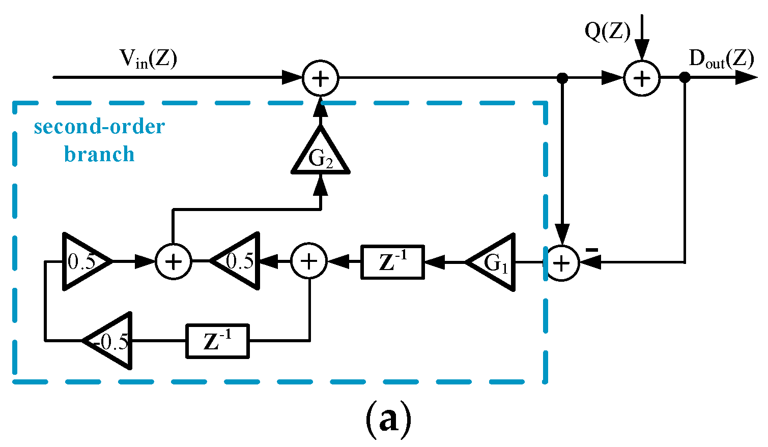
2. System Overview
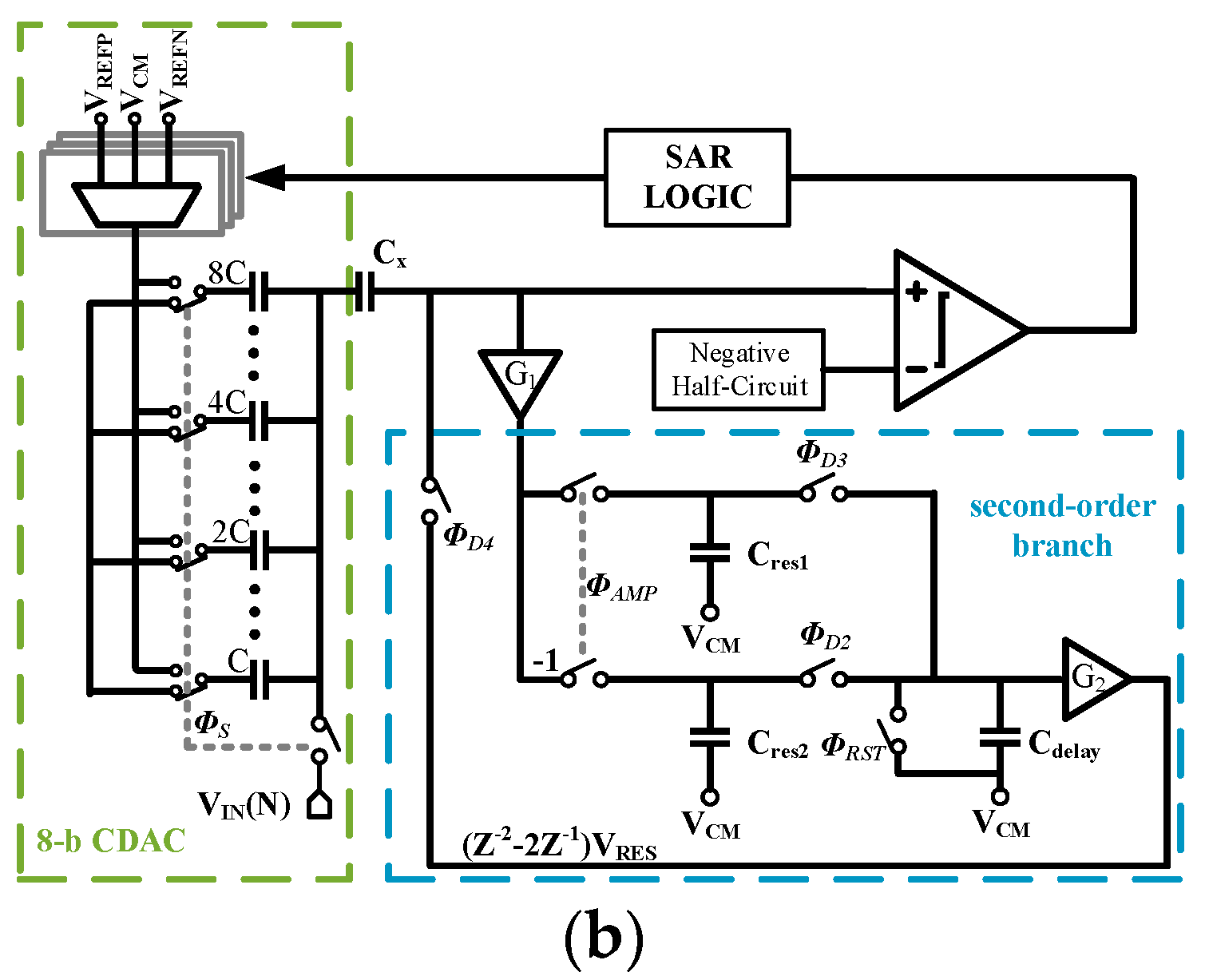
2.1. The Architecture of the Proposed ADC
2.2. System Hybrid Model
3. Circuit Implementation
3.1. The Dynamic Amplifier
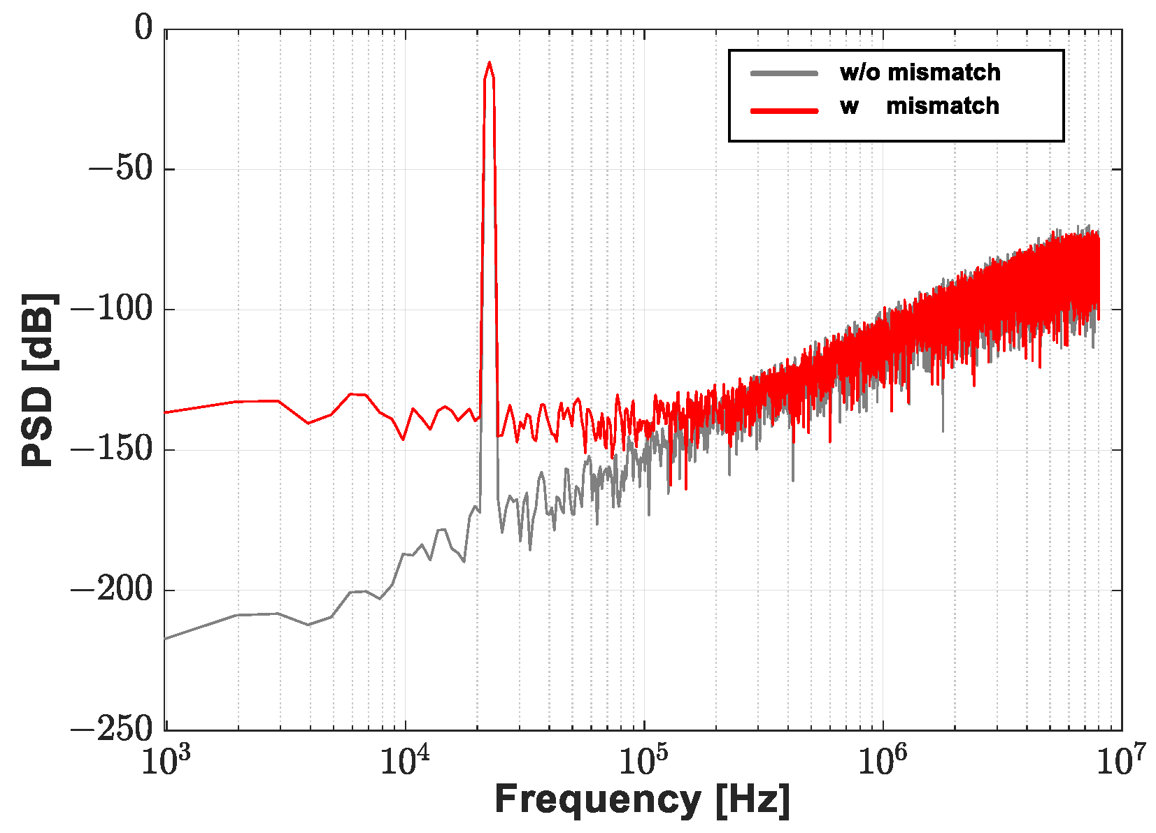
3.2. Nonlinearity Caused by Mismatch Error
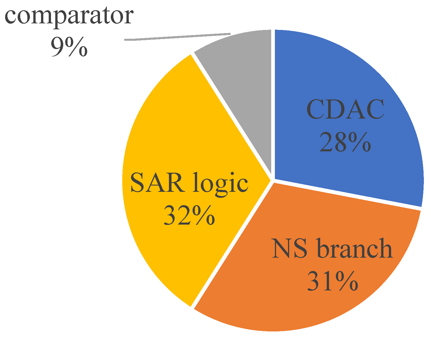
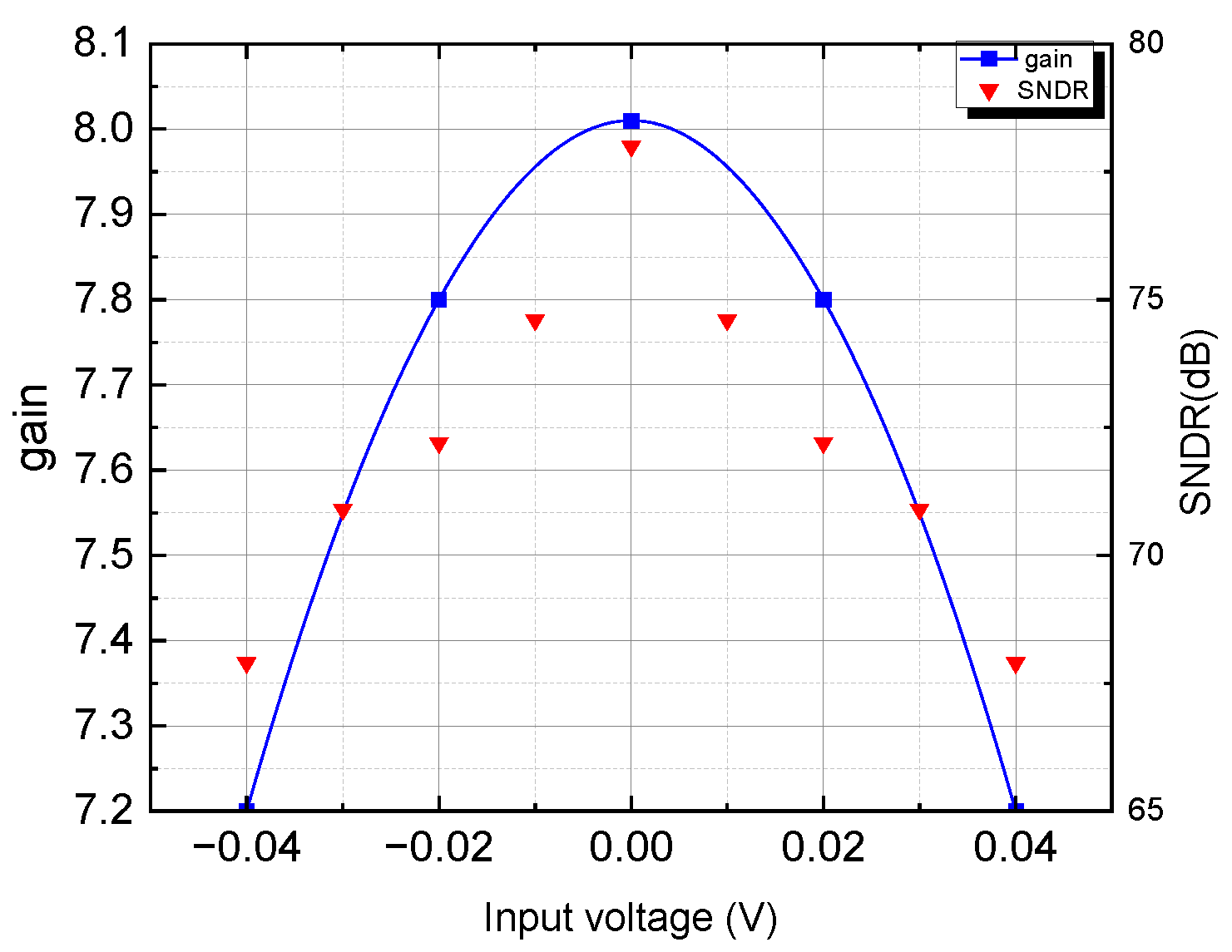
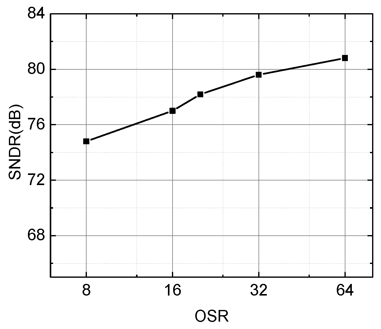
4. Post Simulation and Results
5. Discussion
Author Contributions
Funding
Data Availability Statement
Conflicts of Interest
References
- Guo, W.; Sun, N. A 12b-ENOB 61µW noise-shaping SAR ADC with a passive integrator. In Proceedings of the ESSCIRC Conference 2016: 42nd European Solid-State Circuits Conference, Lausanne, Switzerland, 12–15 September 2016; pp. 405–408. [Google Scholar]
- Chen, Z.; Miyahara, M.; Matsuzawa, A. A 2 nd order fully-passive noise-shaping SAR ADC with embedded passive gain. In Proceedings of the 2016 IEEE Asian Solid-State Circuits Conference (A-SSCC), Toyama, Japan, 7–9 November 2016; pp. 309–312. [Google Scholar]
- Ghaedrahmati, H.; Zhou, J. 160 MS/s 20 MHz bandwidth third-order noise shaping SAR ADC. Electron. Lett. 2018, 54, 128–130. [Google Scholar] [CrossRef]
- Song, Y.; Chan, C.-H.; Zhu, Y.; Geng, L.; Seng-Pan, U.; Martins, R.P. Passive noise shaping in SAR ADC with improved efficiency. IEEE Trans. Very Large Scale Integr. (VLSI) Syst. 2017, 26, 416–420. [Google Scholar] [CrossRef]
- Fredenburg, J.A.; Flynn, M.P. A 90-ms/s 11-mhz-bandwidth 62-db sndr noise-shaping sar adc. IEEE J. Solid-State Circuits 2012, 47, 2898–2904. [Google Scholar] [CrossRef]
- Liu, C.C.; Huang, M.C. 28.1 A 0.46 mW 5MHz-BW 79.7 dB-SNDR noise-shaping SAR ADC with dynamic-amplifier-based FIR-IIR filter. In Proceedings of the 2017 IEEE International Solid-State Circuits Conference (ISSCC), San Francsico, CA, USA, 5–9 February 2017; pp. 466–467. [Google Scholar]
- Li, S.; Qiao, B.; Gandara, M.; Pan, D.Z.; Sun, N. A 13-ENOB second-order noise-shaping SAR ADC realizing optimized NTF zeros using the error-feedback structure. IEEE J. Solid-State Circuits 2018, 53, 3484–3496. [Google Scholar] [CrossRef]
- Jie, L.; Zheng, B.; Flynn, M.P. 20.3 A 50 MHz-bandwidth 70.4 dB-SNDR calibration-free time interleaved 4th-order noise-shaping SAR ADC. In Proceedings of the 2019 IEEE International Solid-State Circuits Conference-(ISSCC), San Francisco, CA, USA, 17–21 February 2019; pp. 332–334. [Google Scholar]
- Baek, J.; Lee, J.; Kim, J.; Chae, H. 2nd-Order Pipelined Noise-Shaping SAR ADC Using Error-Feedback Structure. Electronics 2022, 11, 3072. [Google Scholar] [CrossRef]
- Ijaz, K.; Adnan, M.; Toor, W.T.; Butt, M.A.; Idrees, M.; Ali, U.; Hassan, I.; Ghadi, Y.Y.; Awwad, F.A.; Abonazel, M.R.; et al. A New Noise Shaping Approach for Sigma-Delta Modulators Using Two-Stage Feed-Forward Delays and Hybrid MASH-EFM. Electronics 2023, 12, 740. [Google Scholar] [CrossRef]
- Zhuang, H. A Second-Order Noise-Shaping SAR ADC With Passive Integrator and Tri-Level Voting. IEEE J. Solid-State Circuits 2019, 54, 1636–1647. [Google Scholar] [CrossRef]
- Zhang, Y.; Liu, S.; Tian, B.; Zhu, Y.; Chan, C.-H.; Zhu, Z. A 2nd-Order Noise-Shaping SAR ADC with Lossless Dynamic Amplifier Assisted Integrator. IEEE Trans. Circuits Syst. II Express Briefs 2020, 67, 1819–1823. [Google Scholar] [CrossRef]
- Zhuang, H.; Liu, J.; Tang, H.; Peng, X.; Sun, N. A Fully Dynamic Low-Power Wideband Time-Interleaved Noise-Shaping SAR ADC. IEEE J. Solid-State Circuits JSSC 2021, 56, 2680–2690. [Google Scholar] [CrossRef]
- Baek, J.; Chae, H. A 600-MS/s, 65-dB SNDR, 75-MHz BW Time-Interleaved Noise-Shaping SAR ADC. IEEE Trans. Circuits Syst. II Express Briefs TCSII 2023, 70, 2315–2319. [Google Scholar] [CrossRef]


| Paper | ISSCC 2019 [8] | JSSC 2019 [11] | TCAS-II 2020 [12] | JSSC 2021 [13] | TCAS-II 2023 [14] | This Work |
|---|---|---|---|---|---|---|
| Process (nm) | 40 | 40 | 65 | 40 | 28 | 65 |
| Supply (V) | 1 | 1.1 | 1.2 | 1.1 | 1.1 | 1 |
| Area (mm2) | 0.061 | 0.04 | 0.483 | 0.125 | 0.0387 | 0.122 |
| Resolution (Bit) | 10 | 9 | 8 | 10 | 8 | 8 |
| NS order | 4 | 2 | 2 | 2 | 1 | 2 |
| Fs (MHz) | 400 | 8.4 | 100 | 400 | 600 | 16 |
| OSR | 4 | 16 | 16 | 6 | 4 | 16 |
| Bandwidth (MHz) | 50 | 0.262 | 3.125 | 33.3 | 75 | 0.5 |
| SNDR (dB) | 70.4 | 78.4 | 77 | 73.7 | 65.37 | 78 |
| Power (mW) | 13 | 0.143 | 1.24 | 8.5 | 4.015 | 0.417 |
| FoMs | 166.3 | 171 | 171 | 169.6 | 168.1 | 168 |
Disclaimer/Publisher’s Note: The statements, opinions and data contained in all publications are solely those of the individual author(s) and contributor(s) and not of MDPI and/or the editor(s). MDPI and/or the editor(s) disclaim responsibility for any injury to people or property resulting from any ideas, methods, instructions or products referred to in the content. |
© 2023 by the authors. Licensee MDPI, Basel, Switzerland. This article is an open access article distributed under the terms and conditions of the Creative Commons Attribution (CC BY) license (https://creativecommons.org/licenses/by/4.0/).
Share and Cite
Cui, D.; Wang, Z.; Jiang, M.; Chen, Z. A 78 dB 0.417 mW Second-Order NS SAR ADC with Dynamic Amplifier-Assisted Integrator. Electronics 2024, 13, 371. https://doi.org/10.3390/electronics13020371
Cui D, Wang Z, Jiang M, Chen Z. A 78 dB 0.417 mW Second-Order NS SAR ADC with Dynamic Amplifier-Assisted Integrator. Electronics. 2024; 13(2):371. https://doi.org/10.3390/electronics13020371
Chicago/Turabian StyleCui, Dingkang, Zhihai Wang, Mengqian Jiang, and Zhijie Chen. 2024. "A 78 dB 0.417 mW Second-Order NS SAR ADC with Dynamic Amplifier-Assisted Integrator" Electronics 13, no. 2: 371. https://doi.org/10.3390/electronics13020371