Abstract
Printing electronics is emerging as one of the fastest-growing engineering technologies that are increasingly used and reliable. It provides an alternative to manufacturing electronics devices based on silicon compounds. This article discusses its challenges, problems, and ways of obtaining desired features efficiently and inexpensively. The influence of the most important parameters of the drop-on-demand (DOD) inkjet printing process on the quality of the conductive layers, together with the results of their ageing tests, is illustrated and discussed in terms of their applicability to general-purpose electronics circuits.
1. Introduction
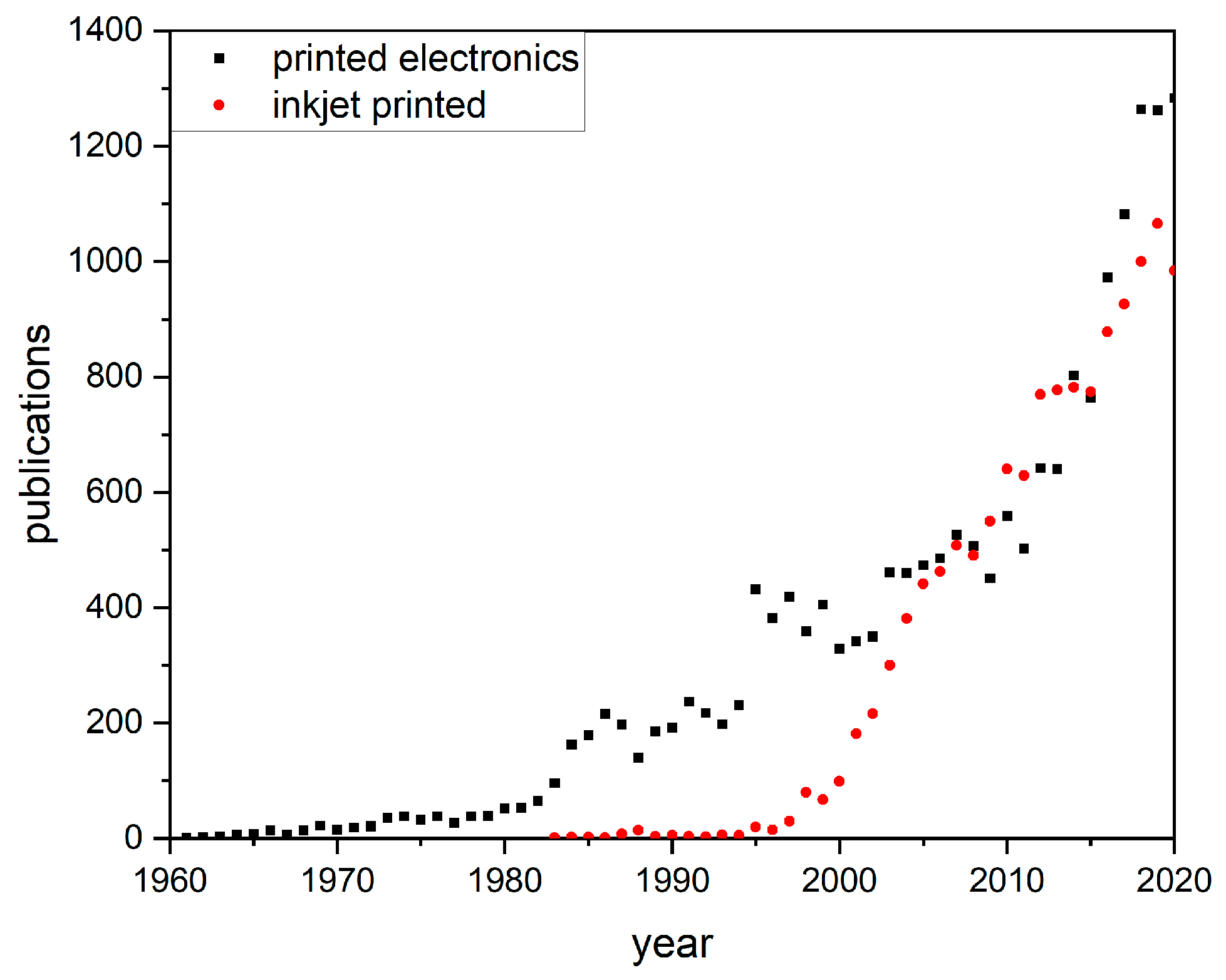
Printed electronics combine many areas of technological research, which may include (micro)electronics, chemistry, and printing. Literature reviews on this subject show a growing interest in this field, which is evidenced by an increasing number of publications that appear in various scientific databases year by year (Figure 1). Analysis of Figure 1 shows that especially after year 2000, the number of published papers with the keywords ‘printed electronics’ or ‘inkjet printing’ has demonstrated a sharply increasing trend.

Figure 1.
Number of publications with keywords: printed electronics, inkjet printing. Based on Scopus [1].
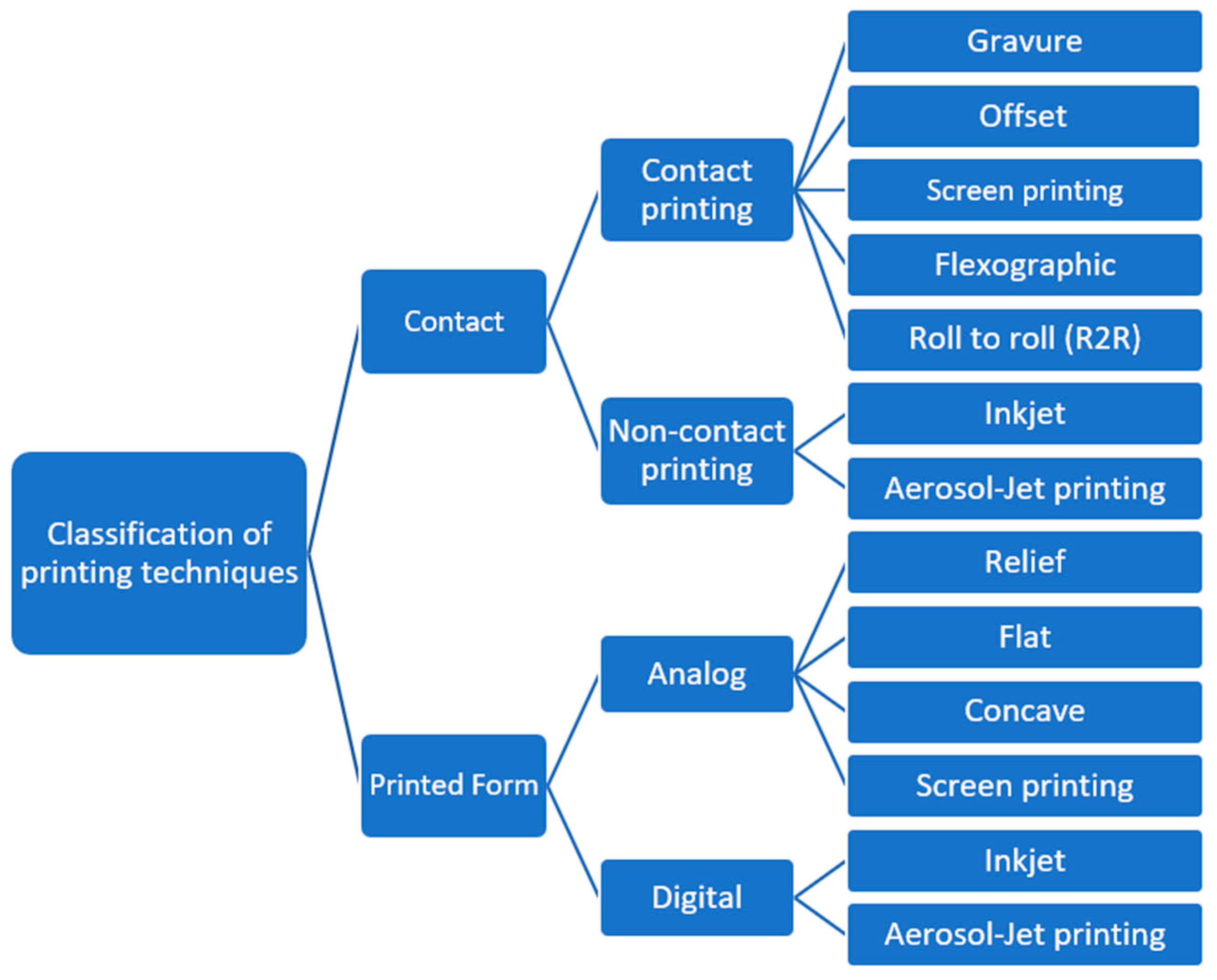
Printing methods can be divided into different categories. The taxonomy of the printing methods is presented in Figure 2.

Figure 2.
Classification of printing techniques.
First, the contact of ink and stencil with the substrate should be considered, which results in contact or non-contact printing, which must be distinguished. Contact printing techniques include [2,3] gravure printing, offset printing, flexographic printing, roll-to-roll (R2R) printing, and screen printing. The most common non-contact printing techniques include inkjet printing and aerosol-jet printing. Non-contact techniques have great appeal due to their unique characteristics of speed, simplicity, high pattern resolution, and easy control, due to the possibility of using different process parameters [2]. A key advantage of most printing techniques (e.g., screen printing, jet printing) is the reduction in material waste, because ink used is applied only where it should be. Any remaining material is collected, and reuse is possible [2].
Within the analog printing technique, the image carrier is the printed form (that is, the corresponding composition of printing and non-printing parts), which in the printing process itself requires the form to be pressed against the substrate. In the literature, impact printing can also be found as a synonym for this printing technique. In digital technology, the information carrier is a digital file. The English-language literature uses the phrases computer-to-printing, digital printing, and non-impact printing. A characteristic feature is that this type of printing does not require the use of a printing form, which therefore makes it possible to print low volumes, which are not very economical in the case of traditional printing. Within analog printing technology, one can distinguish between the following printing forms [4]: relief (i.e., letterpress, flexography), flat (offset), concave (i.e., rotogravure, intaglio, pad printing), and screen printing.
Inkjet printing is a technique that is increasingly being used for the additive manufacturing of electronic and photonic devices. It is characterized by low amounts of waste and the use of a small amount of material needed for the process. Application areas for printed electronics include, so far, resistors [5], organic light-emitting diodes (OLEDs) [6], display [7], solar cells [8], thin-film transistors [9], capacitors [10,11], microwave circuits [12,13], and many others.
However, the application of printed electronics requires the solution of several research problems that include the preparation of substrates and the selection of appropriate printing parameters using selected printing inks. Another problematic issue is the parameters of layer sintering, and how to perform electrical measurements. Printed layers are susceptible to damage (scratching), so appropriate measurement methods must be used. Gieva et al. [14] used a modified Van der Pauw method to measure elastic structures, which allows rapid evaluation of printed conductive structures. Zikulnig et al. [15] also used the Van der Pauw method to determine the resistance of printed silver patterns on paper substrates. In the literature, some examples of publications can be found that describe different issues related to inkjet printing, such as individual drops [16,17], individual layers [18], and modelling [19,20]; the results of studies describe the influence of different factors (e.g., wettability) [21] to indicate the possibility of printing structures with fewer defects. For example, Lorwongtragool et al. studied the morphology of printed lines [22]. Sowadre [23] points out errors such as unwanted drops that cause short circuits or single drops around the print. The study also found problems with wettability and the appearance of dust on the prints. Errors caused by the instability of the ejected ink and too-fast evaporation of the solvent were discussed in [24]. Also, the lack of continuity of the printed layer was analyzed in [23,25]. Another challenge is the appearance of “coffee rings” that make edges thicker than the center of the printed structure. This affects electrical and optical parameters, as well as the formation of subsequent layers printed on structures with this feature.
The use of flexible substrates presents greater opportunities for printed electronics relative to silicon electronics [26]. One of the basic layers is the conductive layer, i.e., that of contacts and interconnections, which are essential components of almost every electronic circuit. A good alternative to lithographic techniques is the use of jet printing [27]. It shortens the processing time, reduces the number of steps, and generates fewer post-production wastes. For printing conductive layers, metal nanoparticle inks are used mainly [28]. The main criteria for selecting compounds for nanoparticles are price, volume resistance, and ease of storage and handling. Silver nanoparticles are usually used. A cheap and highly conductive alternative to silver is copper; however, copper nanoparticles can easily spontaneously oxidize when exposed to air [29]. Another example of a good candidate for a conductive material is gold; however, its price is relatively high.
One of the important aspects of printing conductive structures using the streaming technique is the need to create a functional conductive layer from liquid ink. This involves subjecting the printed pattern to a treatment that ensures functionality. One of the cheapest and most popular methods is sintering at elevated temperatures [30]. At curing temperature, the metal particles lose their coating and begin to conduct through direct contact with each other. Sintering, on the other hand, which is characterized by higher temperatures than curing, occurs when all of the organic material evaporates and necks begin to form between the metal nanoparticles. The evaporation of the solvent is associated with the fact that individual nanoparticles come close to each other. Electrical conduction occurs only when metallic contact between particles occurs and relocation layers are formed throughout the material [31].
To achieve low resistance of the printed layers, it is necessary to transform small contact areas of the interparticle necks into large and thick necks, resulting in a homogeneous layer. Sintering can occur at a lower temperature than the melting process of the material. For example, solid silver melts at 960 °C, while the classical sintering process of conductive layers requires temperatures of more than 200 °C [32].
This sintering temperature is not always compatible with common polymer foils that could be used as substrates, i.e., polycarbonate (PC) and polyethylene terephthalate (PET). Such foils have a low glass transition temperature, leading to substrate damage, deformation, and destruction.
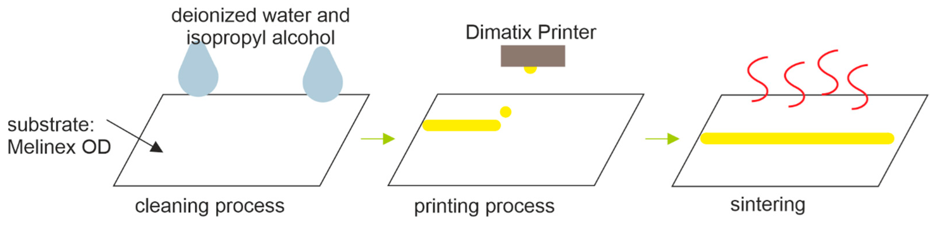
The inkjet printing process consists of three basic steps: cleaning, ink deposition, and sintering. The key to obtaining reproducible structures with good quality is the proper selection of parameters at each step of structure preparation [33]. Important parameters of the printing process itself include drop space, number of nozzles, head height, cartridge temperature, and waveform.
The main objective of the present research was to analyze the possibility of manufacturing selected microelectronic structures using inkjet printing, while minimizing the financial outlay for the entire technological process by using the cheapest possible available substrates and the cheapest possible commercially available ink. Therefore, the drop space, the height of the head above the substrate, the temperature of the printing table, the sintering time, and the temperature were changed during the tests to analyze their influence on the quality of prepared structures. A good quality layer is a structure in which there are no defects or discontinuities, and the desired shape is maintained. Obtaining homogeneous layers is quite a problem and a challenge for technology [34,35].
Several important parameters affect the quality of prints. Among the most important are drop space, cartridge height above the substrate, table temperature, time, and curing temperature. In inkjet printing, the drop space parameter refers to the distance between successive drops of ink in a jet that falls on the surface of the printed material. The impact of this parameter on the printing process can be significant, and the optimal drop space value depends on several factors. There are some aspects to consider, such as print resolution: drop space has a direct impact on print resolution. Too little drop space can lead to overlap in the printing pattern, which can distort the structure and make it difficult to achieve sharp detail.
On the other hand, too much distance can affect pattern quality and detail, as exemplified by discontinuities. Optimal drop space distance can improve image quality by controlling the spread of droplets and the leveling of undesirable defects (discontinuities or short circuits). Drop space also affects printer performance. Too little drop space can lead to a slower printing process because the printer needs more time to recharge with ink. Too much distance, on the other hand, can increase printing speed, but this can come at the expense of quality.
Heating the table also affects the quality of the layers. The right table temperature affects the quality of the printed surface. As printing inks are based on solvents, the heating of the substrate is one of the key parameters. Heating too fast can lead to a “coffee ring” and unevenness, and heating too slow makes it impossible to maintain the desired pattern.
Temperature and curing time also affect the quality of the layers. This is a key parameter, especially since it directly affects the electrical parameters obtained by this layer. Too low a temperature will cause the sintering process to fail, while too high a temperature can interact negatively with the substrate, causing deformation. It should also be borne in mind that temperature-sensitive substrates are used for jet printing. Too high a temperature can cause the substrate to decohere.
2. Materials and Methods
A schematic view of the manufacturing process using inkjet printing applied in this study is presented in Figure 3. A Melinex OD foil (DuPont Teijin Films, Contern, Luxemburg) with a thickness of 125 μm was used as a substrate. The most important film parameters are the elongation at break (125%), the total luminous transmission (89.5%), and the dielectric strength (125 kV/mm) [36]. Amepox Nano Ink AX JP-60n (Amepox, Konstantynów Łódzki, Poland) ink was chosen as the printing ink. The samples were printed using a Dimatix 2831 printer (from Fujifilm Dimatix, Santa Clara, CA, USA) and a 10 pL print head. A Binder GmbH (Tuttlingen, Germany) convection oven was used for sintering the structures. A Hewlett Packard 4263A LCR (Hewlett-Packard Company, Palo Alto, CA, USA) meter was used for electrical measurement, and a Carl Zeiss Axio Vision microscope (Carl Zeiss, Jena, Germany) and AxioVision software (version 4.5, Carl Zeiss, Jena, Germany) was used for optical observation. For the ageing tests, a Binder MKF-115 (Tuttlingen, Germany) climate chamber was used.

Figure 3.
The inkjet printing process.
The substrates were first cleaned with deionized water in a Branson 8210 (Branson Ultrasonics Corporation, Danbury, CT, USA) ultrasonic cleaner for 10 min, and then dried at room temperature for 15 min (Figure 3). After that, the substrates were again placed in an isopropyl alcohol ultrasonic washer and cleaned for 10 min. Finally, the substrates were dried at room temperature for 10 min. The pattern (12 mm × 1 mm) was printed on the substrates prepared this way.
Some 45 series of test samples, with 10 pieces in each series, were prepared, in which drop space, head height, table temperature, time, and sintering temperature were changed. For the drop space parameter, six measurement series were printed (5 μm, 10 μm, 15 μm, 20 μm, 25 μm, and 30 μm). For different head heights, 21 measurement series were prepared (with distances from 50 μm to 600 μm in increments of 50 μm, and from 600 μm to 1500 μm in increments of 100 μm). The table temperature was changed from room temperature (23 °C to 60 °C) with steps of 5 °C from 30 °C. There were four different sintering times (20, 40, 60, and 80 min) at temperatures ranging from 120 °C to 170 °C with steps of 10 °C. The exact parameters and test conditions are summarized in Table 1. Research began with the selection of appropriate printing parameters by, among other things, analyzing the drop space parameter. The effect of cartridge height on the quality of the print was then analyzed. In the next step, the effect of table temperature during printing was checked. The final step was to analyze the temperature and the sintering time.

Table 1.
Conditions of test series.
3. Results
3.1. The Effect of the Drop Space
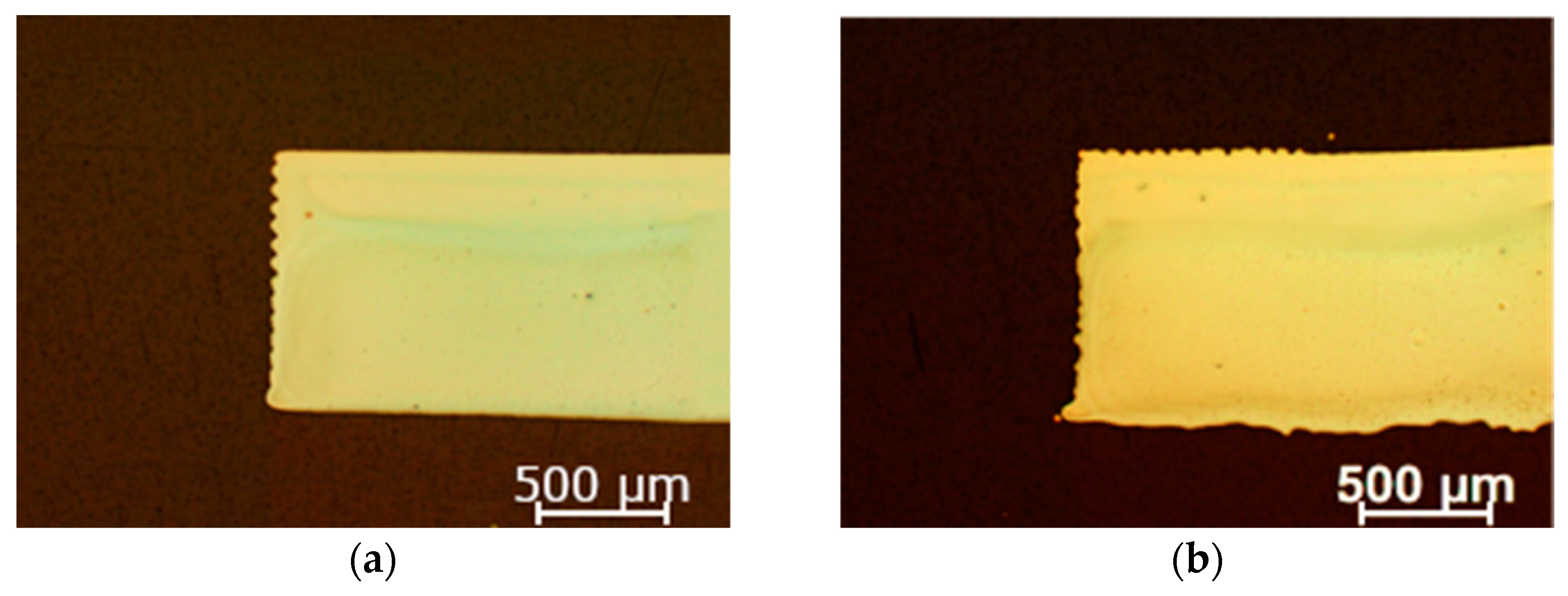
Microscopic images of silver lines printed with different droplet spacing are shown in Figure 4. The line width is inversely proportional to the spacing of the droplets [37]. Too little drop space will make the pattern continuous, but not uniform. Also, the printed layer will be thicker, and the ink will spill beyond the limits of the desired pattern, so the reproduction and quality of the print will not be good enough. It is also important that the printing time increases as the value of the drop space parameter decreases. On the other hand, too much drop space will make the pattern discontinuous. In the case of the Fujifilm Dimatix Materials Printer DMP-2831, the droplet spacing could be varied from 5 to 254 μm. During the study, the parameter was changed from 5 μm to 30 μm. Further increases in the drop space made the pattern less and less homogeneous, and there were voids due to the lack of ink. Exemplary microscopic images of silver lines printed with different drop spaces are shown in Figure 4. The research conducted indicated that the optimal drop space is 15 µm.
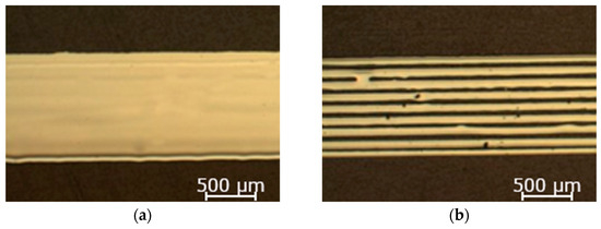
Figure 4.
Microscopic images of lines with different drop spaces: (a) 15 µm and (b) 25 µm.
3.2. The Effect of the Cartridge Height
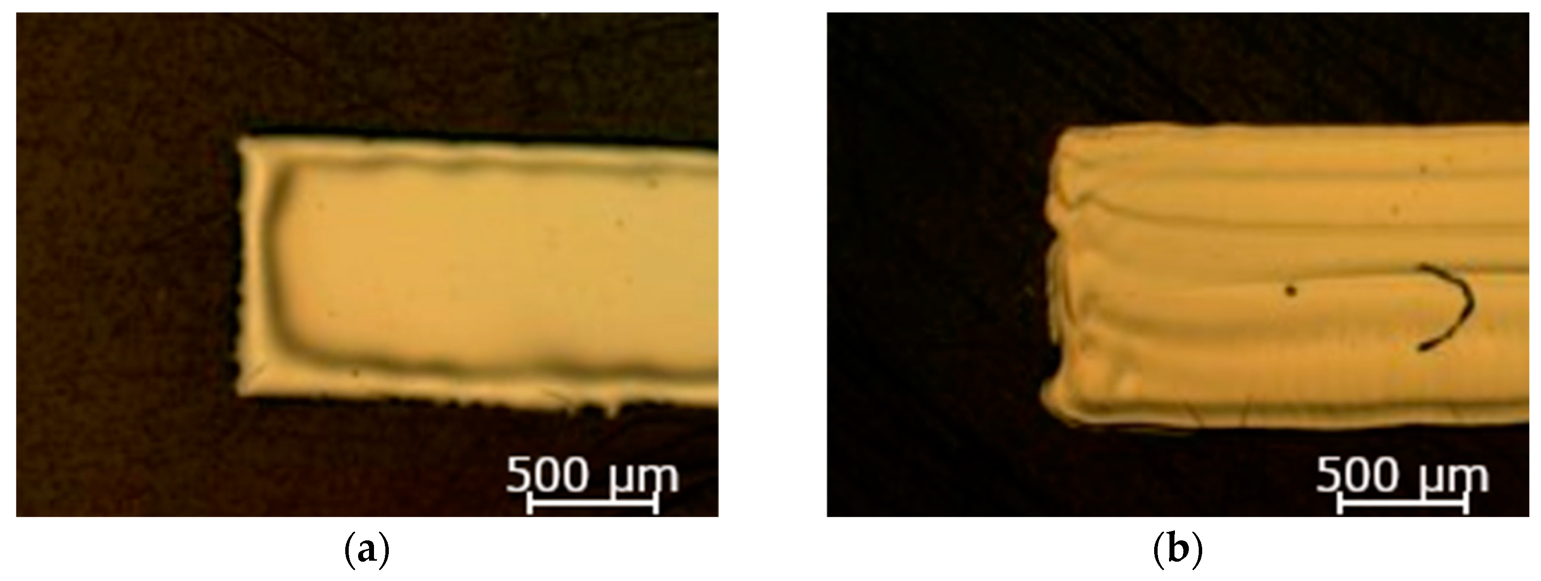
Another important parameter from the point of view of the quality of printed layers is the height of the head above the substrate level. If it is too high, it does not maintain the desired shape, because there is waviness on the edge, and unwanted droplets form as a result of ink splashing on the substrate. If the height is too low, it can result in jamming of the carriage with the table cartridge. Additionally, this can result in the smearing of the pattern as a result of the movement of the carriage. The height of the head must be selected for the rheology of the ink ejected from the cartridge [38]. In the case of the Fujifilm Dimatix Materials Printer DMP-2831, the height of the carriage above the printer table can be up to 25 mm. During the tests, the parameter was changed from 50 μm to 1500 μm (up to 600 μm in 50 μm increments, and from 600 μm upwards in 100 μm increments) over the height of the Melinex OD film on the substrate (not the printer table). With further increase in the droplet spacing, the pattern became less and less distinct, and there was more splatter of material around the desired shape. Exemplary microscopic images of silver lines printed at different heights of the cartridge above the substrates are shown in Figure 5. As can be seen in the figure, the shape of the print surface and edge depends on the height. The research conducted indicated that the optimal cartridge height is 50 µm.
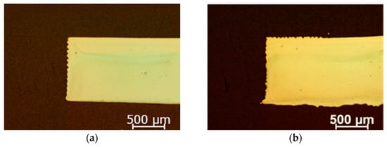
Figure 5.
Microscopic images of lines with different cartridge heights: (a) 50 µm and (b) 1000 µm.
3.3. The Effect of Table Temperature
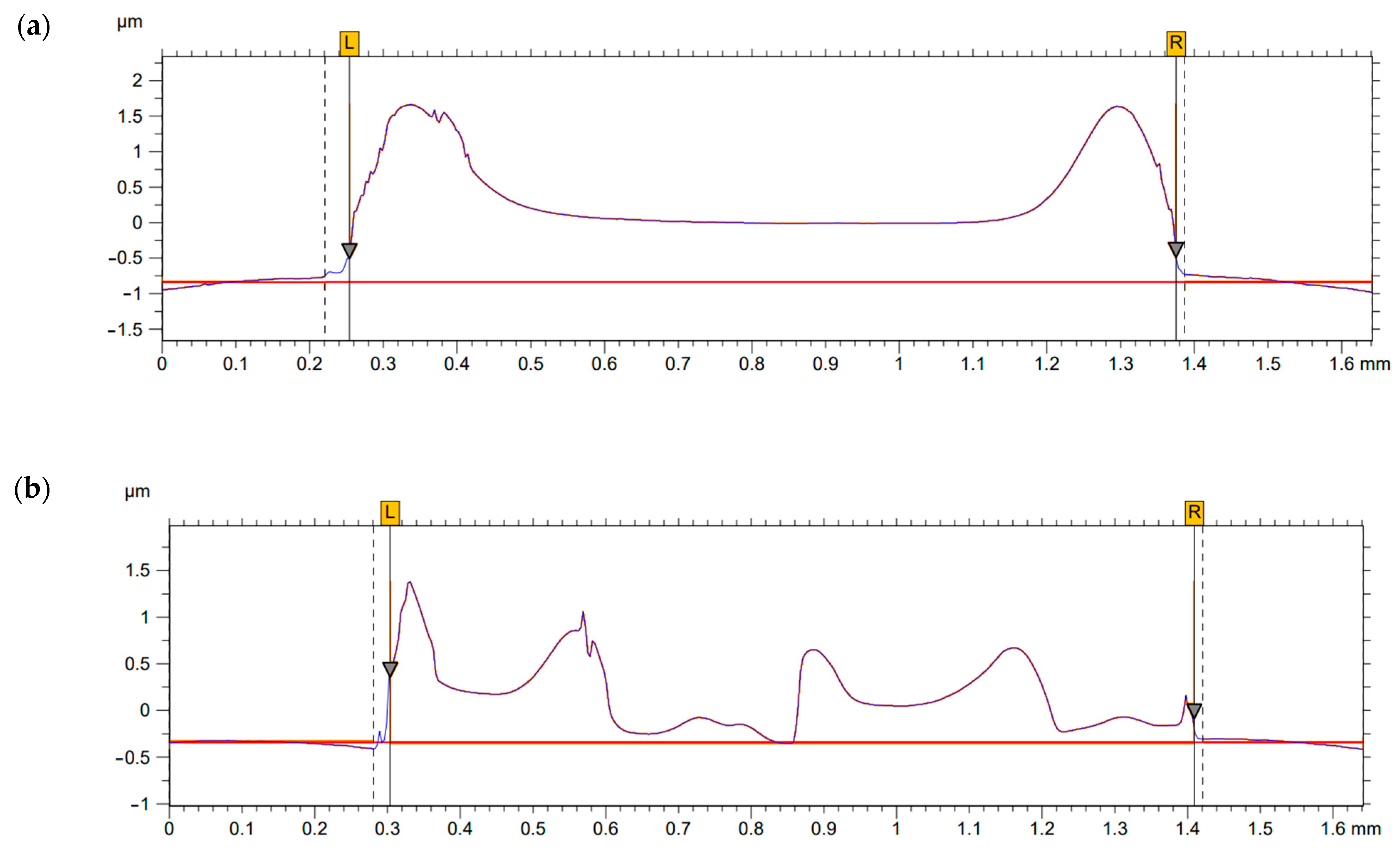
Another important parameter is the temperature of the table. At a lower temperature, the coffee ring is even on both sides of the layer, while at a higher temperature, there are visible differences in height (especially at the edge). The unevenness is related to the evaporation of the solvent during the printing process. Too low a temperature also causes the printed layer to be transferred to the convection oven for sintering, causing the ink to spread. When printing, especially on polymer substrates, it is recommended to accelerate the solvent evaporation process using a heating table [39]. In the case of the Fujifilm Dimatix Materials Printer DMP-2831, the table temperature can be changed from room temperature to 60 °C. The study analyzed the effect of different table temperatures on print quality. The first batch was printed with the heating turned off, so it can be assumed that it was at room temperature—about 23 °C. This is quite inaccurate, so the first possible temperature was set to 30 °C. Then, it was increased in increments of 5 °C until it reached 60 °C. Microscopic images of silver lines printed at different table temperatures are shown in Figure 6. As can be seen in the figure, at higher temperatures, the morphology and shape of the line are more heterogeneous. At lower temperatures, the coffee ring effect is more pronounced. These observations are also confirmed by tests performed with a mechanical profilometer (Figure 7).
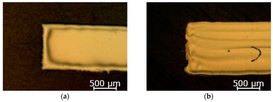
Figure 6.
Microscopic images of lines with different table temperatures: (a) 30 °C and (b) 60 °C.
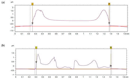
Figure 7.
Profilogram of lines prepared using different table temperatures: (a) 30 °C and (b) 60 °C.
3.4. The Effect of Temperature and Sintering Time on Electrical Resistance
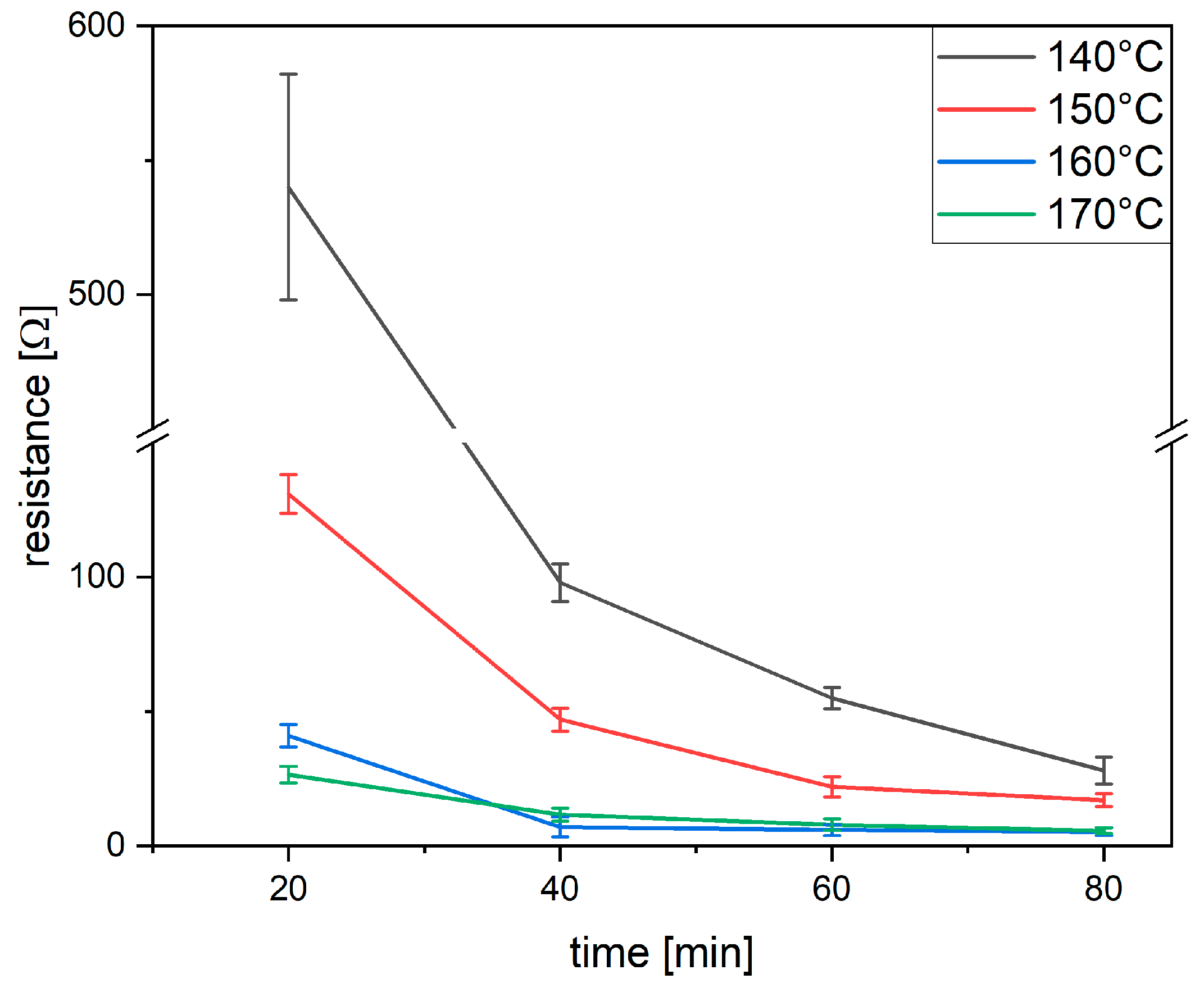
Each sintering process consists of three basic steps: heating, curing, and cooling. This study involved a 4 °C/min build-up and cooling in a closed convection oven. This study also involved changes to the time and temperature of the curing stage. The times analyzed were 20, 40, 60, and 80 min at temperatures ranging from 120 to 170 °C in 10-degree increments. Increasing the temperature further was not possible due to the high shrinkage of the film that occurred.
The quantitative parameter which was chosen for investigations of the influence of sintering temperature and time on the printed silver lines quality was electrical resistance. The results of the resistance measurements are collected in Table 2. The high resistance value seen in Figure 8 at the initial stage of the process indicates that no sintering process has occurred between the individual molecules of silver, the base component of the ink. By increasing the sintering temperature, it is possible to observe a decrease in resistance, and therefore an increase in conductivity, which is the result of the occurrence of diffusion processes that result in the formation of neck connections. This results in an increase in the contact area between the nanoparticles. The diffusion processes that occur between the particles cause the pores to close, and after a sufficiently long period, the pores disappear from the structure, resulting in low resistance. Importantly, the longer the sintering process time and the higher the temperature, the lower the final resistance value. A lower sintering temperature prolongs the process of stabilizing the resistance value.
Table 2.
Results of resistance measurements as a function of sintering time and temperature.
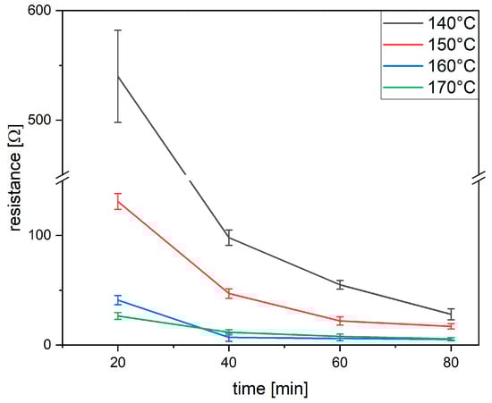
Figure 8.
Influence of temperature and curing time on resistance value.
As can be seen from the analysis of Figure 8, very small resistance values are obtained for a temperature of 160 °C and sintering times of 60 and 80 min. Considering that the substrate used is a Melinex OD film, we decided to choose 160 °C for 60 min.
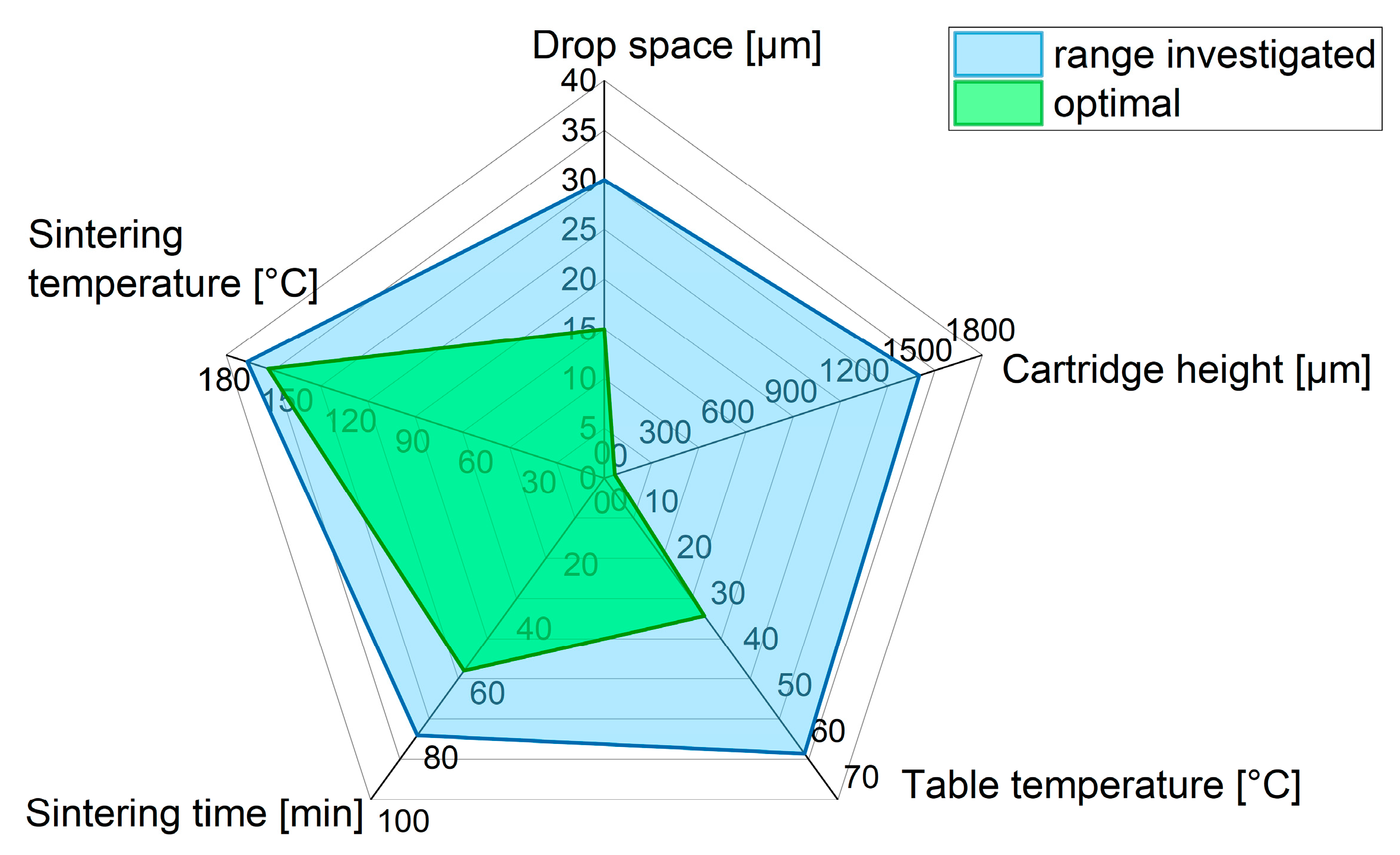
In Figure 9, the analyzed (range investigated) parameters are shown, and the optimal values of the studied quantities are indicated. Thus, it can be read that the best optical-geometric values are obtained by printing with a drop space of 15 µm, a table temperature of 30 °C, and a head height of 50 µm. The best electrical parameters are influenced by sintering time and temperature. The tests performed indicated that the process should be carried out at 160 °C for 60 min.

Figure 9.
Illustration of the analyzed parameters with the indication of optimal values.
3.5. The Effect of Accelerated and Bending Tests on Electrical Parameters
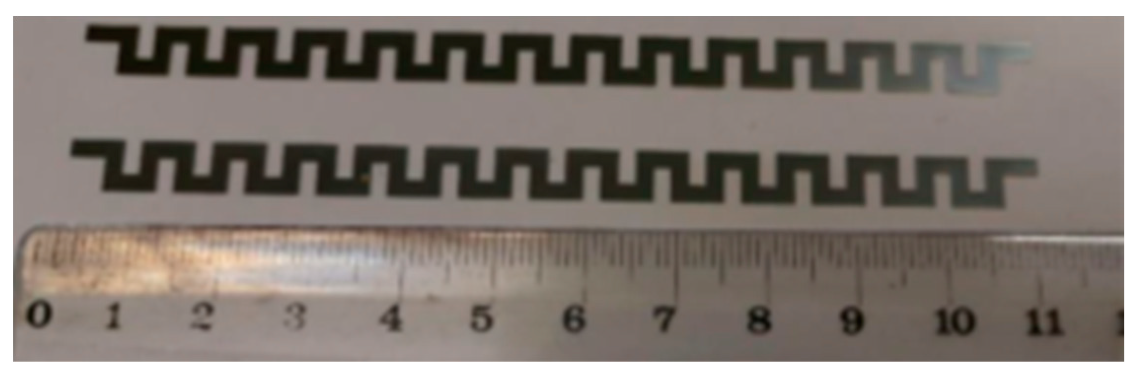
Ageing tests allowed us to determine the influence of humidity and temperature on electrical parameters. The fabricated samples (Figure 10), printed according to the optimal parameters described (drop space 15 μm; table temperature 30 °C, sintering 160 °C/60 min), were continuously subjected to a series of reliability tests in a Binder MKF 115 climate chamber for 125 h. The samples under different conditions were analyzed by changing the temperature and humidity using a combination of these parameters. A total of six different configurations were used, and are denoted by letters a–f, presented in Table 3.
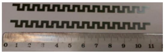
Figure 10.
Test samples for testing in the climate chamber.
Table 3.
Configuration of the temperature–humidity cycles used for testing in the climate chamber.
The tests were conducted at temperatures that negate the interaction with the substrate.
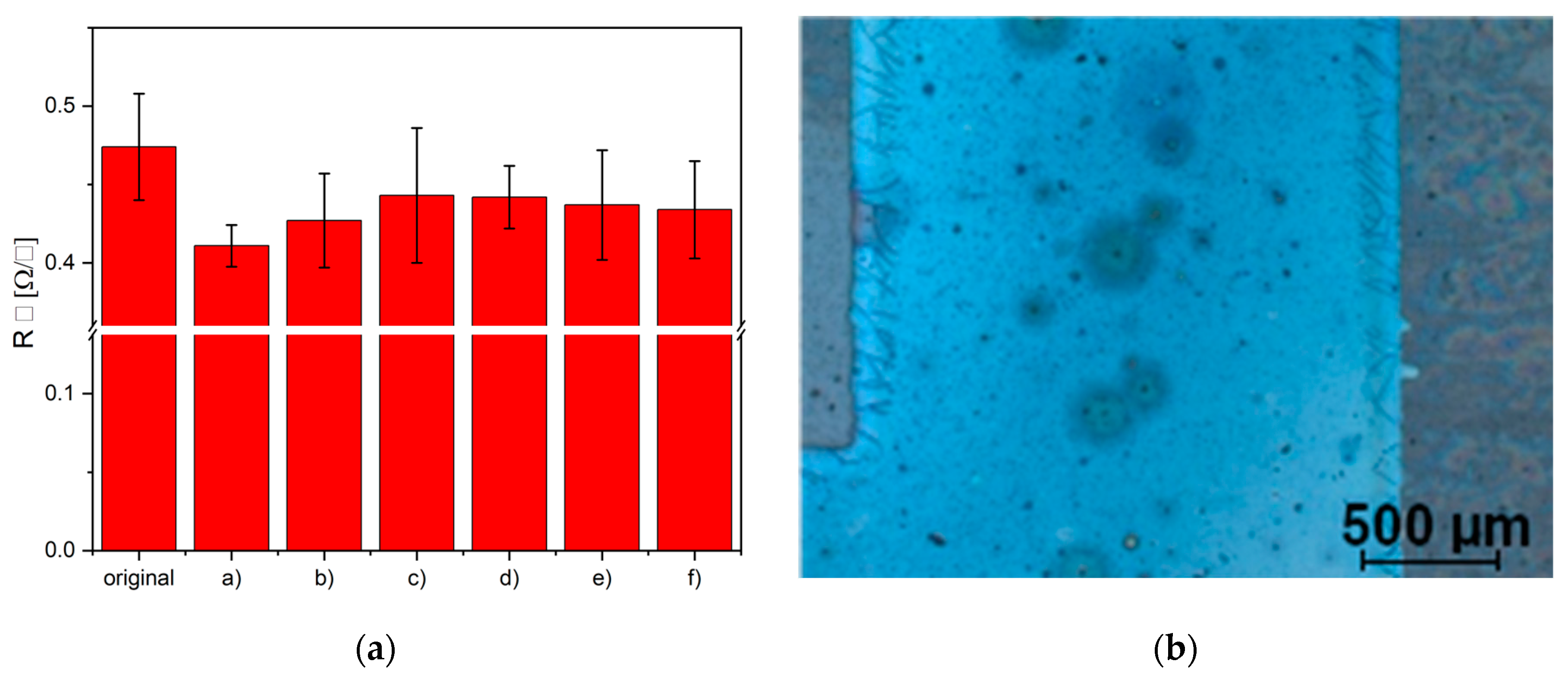
For each of the series of measurements, 10 samples were taken, and the aggregate results of the resistance change are shown in Figure 11a. From the analysis of the results of the tests obtained using the climate chamber, it can be seen that the greatest impact on the change in the resistance values of the tested samples was caused by processes during which there was a change in cyclical temperature. With all tests, the resistance value decreased. An exemplary microscopic image of the structure after the tests (profile a) can be seen in Figure 11b.

Figure 11.
(a) Influence of climatic conditions on the resistance value of the analyzed samples. (a–f) denote different combinations of temperature and humidity; (b) microscopic image showing changes in the structure after climate chamber tests (a).
Analysis of the quality of the conductive layers and the performance of ageing tests made it possible to identify the factors that affect the deterioration of electrical parameters by performing tests in a climate chamber using different temperatures, humidity, and combinations of these parameters. The tests showed that the change in resistance was most influenced by the cyclic change in temperature, as shown in Figure 12a, which shows discoloration, indicating oxidation of the applied layer, while the edges show clear cracks. They contributed to changes in the electrical parameters of the analyzed structures. An explanation of the observed effect of lowering the resistance value could be absorption of moisture (water) during tests in a climate chamber. The absorption of water caused an increase in volume, resulting in micro-cracks in the structure, especially at the edges, where the height of the layer is much bigger due to the coffee ring effect that occurs. Such an effect also indicates the necessity of aging the fabricated structures according to a specific temperature profile, especially when the printed conductive path will be a component of a larger electronic component operating under varying atmospheric conditions. In addition, structures made with the inkjet printing technology should be protected from moisture and rapid temperature changes.
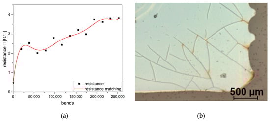
Figure 12.
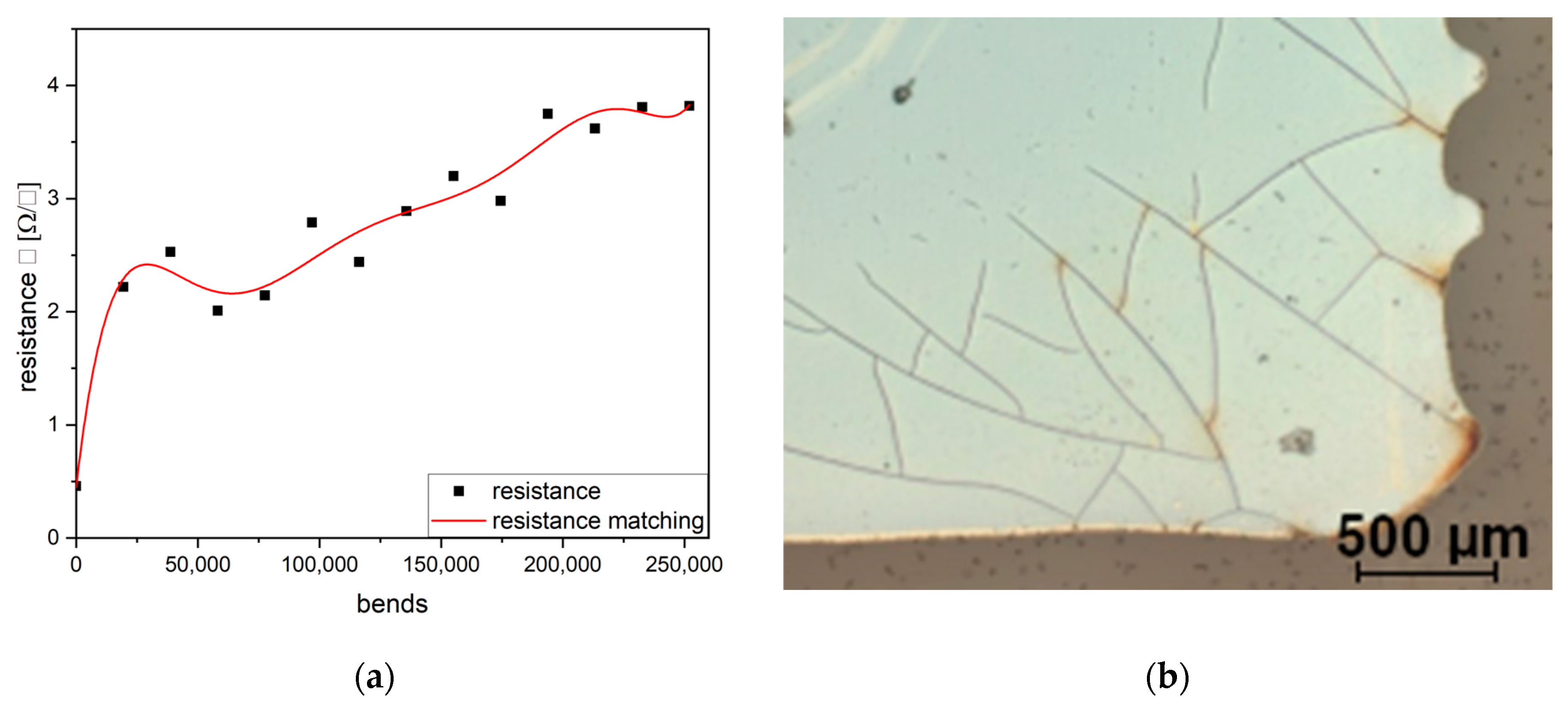
(a) Resistance change during the bending and straightening process; (b) microscopic image showing changes in the structure after bending tests.
The printed structures (the same as for testing in a climate chamber) were bent at a radius of 20.5 mm, in cycles of 100 bends and straightenings per minute. During the tests, which lasted more than 42 h, the resistance of 10 samples was measured, and the resistance value of the flexed structures due to the bending forces was determined. Measurements were made every 3 h, and the results are shown in Figure 12a. From Figure 12a, it can be seen that during the bending and straightening of the samples, the resistance changes in an increasing and decreasing manner, with a tendency for the resistance after each measurement to be greater than the initial resistance. During the tests, there was a change in resistance of more than one order. The largest resistance change was recorded in the first 3 h (a difference of 383% from the initial resistance). In 42 h, the resistance changed by as much as 900%. As one can see in Figure 12b, a possible reason for the observed increase in resistance is due to cracks appearing in the tested samples, and a change in the roughness of the layer. Cracking of the edges of the printed structure is associated with the coffee ring effect, because there is more material on the edges, so it will be subjected to the effects of bending more quickly. Despite the resistance changes observed during the ageing and bending test, it is worth noting that the fabricated conductive structures printed on flexible substrates retain their good mechanical and electrical parameters. No delamination effect was observed, which could exclude the structures from further use.
4. Conclusions
This paper discusses an approach towards the development of a cheap and facile method for the fabrication of conducting lines on a flexible substrate using the inkjet printing method. It was shown that by using low-cost materials (i.e., substrate and ink), it is possible to print repeatable structures, minimizing the possibility of defects that would affect the quality of the designs. The correct selection of parameters makes it possible to obtain repeatable structures. Analysis of the quality of the conductive layers allowed reproducible printing of conductive structures by selecting the appropriate parameters, i.e., substrate temperature, drop space value, sintering time, and temperature. The ageing tests performed showed that there was no delamination of the layers and no critical damage that would prevent the continued operation of the systems. In addition, the layers retained their conductive properties at a good level. The tests confirmed that the layers were printed correctly and that the elaborated curing method was also adequate.
Funding
This work was financed from the internal sources of Wroclaw University of Science and Technology.
Data Availability Statement
The data presented in this study are available on request from the corresponding author.
Conflicts of Interest
The authors declare no conflict of interest.
References
- Available online: https://www.scopus.com/ (accessed on 20 January 2023).
- Khan, S.; Lorenzelli, L.; Dahiya, R.S. Technologies for printing sensors and electronics over large flexible substrates: A review. IEEE Sens. J. 2015, 15, 3164–3185. [Google Scholar] [CrossRef]
- Zikulnig, J.; Chang, S.; Bito, J.; Rauter, L.; Roshanghias, A.; Carrara, S.; Kosel, J. Printed Electronics Technologies for Additive Manufacturing of Hybrid Electronic Sensor Systems. Adv. Sens. Res. 2023, 7, 2200073. [Google Scholar] [CrossRef]
- Suresh, R.R.; Lakshmanakumar, M.; Arockia Jayalatha, J.B.B.; Rajan, K.S.; Sethuraman, S.; Krishnan, U.M.; Rayappan, J.B.B. Fabrication of Screen-Printed Electrodes: Opportunities and Challenges. J. Mater. Sci. 2021, 56, 8951–9006. [Google Scholar] [CrossRef]
- Bidoki, S.M.; Nouri, J.; Heidari, A.A. Inkjet deposited circuit components. J. Micromech. Microeng. 2010, 20, 055023. [Google Scholar] [CrossRef]
- Amruth, C.; Luszczynska, B.; Rekab, W.; Szymanski, M.Z.; Ulanski, J. Inkjet printing of an electron injection layer: New role of cesium carbonate interlayer in polymer oleds. Polymers 2021, 13, 80. [Google Scholar] [CrossRef]
- Kuang, M.; Wang, J.; Bao, B.; Li, F.; Wang, L.; Jiang, L.; Song, Y. Inkjet Printing Patterned Photonic Crystal Domes for Wide Viewing-Angle Displays by Controlling the Sliding Three Phase Contact Line. Adv. Opt. Mater. 2014, 2, 34–38. [Google Scholar] [CrossRef]
- Karunakaran, S.K.; Arumugam, G.M.; Yang, W.; Ge, S.; Khan, S.N.; Lin, X.; Yang, G. Recent progress in inkjet-printed solar cells. J. Mater. Chem. A Mater. 2019, 7, 13873–13902. [Google Scholar] [CrossRef]
- Das, S.; Venkatakrishnan, A.; Yamamoto, H.; Watson, G.P. Fabrication of Organic Thin Film Transistors Using Inkjet Printing of PEDOT:PSS; Singh Center for Nanotechnology: Philadelphia, PA, USA, 2019. [Google Scholar]
- Liu, Y.; Cui, T.; Varahramyan, K. All-polymer capacitor fabricated with inkjet printing technique. Solid. State Electron. 2003, 47, 1543–1548. [Google Scholar] [CrossRef]
- Kiliszkiewicz, M.; Jasińska, L.; Dziedzic, A. The ink-jet printed flexible interdigital capacitors: Manufacturing and ageing tests. Flex. Print. Electron. 2023, 8, 035016. [Google Scholar] [CrossRef]
- Szostak, K.; Słobodzian, P.; Kiliszkiewicz, M.; Jasińska, L.; Slobodzian, P.; Korbutowicz, R.; Malecha, K. Inkjet Printed vs Screen Printed Microstrip Line on LTCC Substrates. In Proceedings of the 2019 Conference on Microwave Techniques (COMITE), Pardubice, Czech Republic, 16–18 April 2019. [Google Scholar] [CrossRef]
- Jasińska, L.; Szostak, K.; Kiliszkiewicz, M.; Słobodzian, P.; Malecha, K. Ink-jet printed ring resonator with integrated Microfluidic components. Circuit World 2020, 46, 301–306. [Google Scholar] [CrossRef]
- Gieva, E.; Nikolov, G.; Nikolova, B. Sheet Resistance Measurement of Inkjet Printed Layers. In Proceedings of the 2019 42nd International Spring Seminar on Electronics Technology (ISSE), Wroclaw, Poland, 15–19 May 2019. [Google Scholar] [CrossRef]
- Zikulnig, J.; Roshanghias, A.; Rauter, L.; Hirschl, C. Evaluation of the Sheet Resistance of Inkjet-Printed Ag-Layers on Flexible, Uncoated Paper Substrates Using Van-der-Pauw’s Method. Sensors 2020, 20, 2398. [Google Scholar] [CrossRef] [PubMed]
- Molina-Lopez, F.; Quintero, A.V.; Mattana, G.; Briand, D.; de Rooij, N.F. Large-area compatible fabrication and encapsulation of inkjet-printed humidity sensors on flexible foils with integrated thermal compensation. J. Micromech. Microeng. 2013, 23, 025012. [Google Scholar] [CrossRef]
- Lohse, D. Fundamental Fluid Dynamics Challenges in Inkjet Printing. Annu. Rev. Fluid Mech. 2022, 54, 349–382. [Google Scholar] [CrossRef]
- Kiliszkiewicz, M.; Przybylski, D.; Felba, J.; Korbutowicz, R. Structural characterization of inkjet printed capacitor layers in various technological conditions. Solder. Surf. Mt. Technol. 2020, 32, 235–240. [Google Scholar] [CrossRef]
- Tan, H.; Torniainen, E.; Markel, D.P.; Browning, R.N.K. Numerical simulation of droplet ejection of thermal inkjet printheads. Int. J. Numer. Methods Fluids 2015, 77, 544–570. [Google Scholar] [CrossRef]
- Hu, S.; Zhu, W.; Yang, W.; Li, M. Morphology simulation of drop-on-demand inkjet-printed droplets. NPJ Flex. Electron. 2022, 6, 64. [Google Scholar] [CrossRef]
- He, B.; Yang, S.; Qin, Z.; Wen, B.; Zhang, C. The roles of wettability and surface tension in droplet formation during inkjet printing. Sci. Rep. 2017, 7, 11841. [Google Scholar] [CrossRef]
- Lorwongtragool, P.; Sowade, E.; Watthanawisuth, N.; Baumann, R.R.; Kerdcharoen, T. A novel wearable electronic nose for healthcare based on flexible printed chemical sensor array. Sensors 2014, 14, 19700–19712. [Google Scholar] [CrossRef]
- Sowade, E.; Ramon, E.; Mitra, K.Y.; Martínez-Domingo, C.; Pedró, M.; Pallarès, J.; Loffredo, F.; Villani, F.; Gomes, H.L.; Terés, L.; et al. All-inkjet-printed thin-film transistors: Manufacturing process reliability by root cause analysis. Sci. Rep. 2016, 6, 33490. [Google Scholar] [CrossRef]
- Mitra, K.Y.; Sowade, E.; Martínez-Domingo, C.; Ramon, E.; Carrabina, J.; Gomes, H.L.; Baumann, R.R. Potential up-scaling of inkjet-printed devices for logical circuits in flexible electronics. AIP Conf. Proc. 2014, 1646, 106–114. [Google Scholar] [CrossRef]
- Abbel, R.; Teunissen, P.; Rubingh, E.; Van Lammeren, T.; Cauchois, R.; Everaars, M.; Valeton, J.; Van De Geijn, S.; Groen, P. Industrial-scale inkjet printed electronics manufacturing—Production up-scaling from concept tools to a roll-to-roll pilot line. Transl. Mater. Res. 2014, 1, 015002. [Google Scholar] [CrossRef]
- Leenen, M.A.M.; Arning, V.; Thiem, H.; Steiger, J.; Anselmann, R. Printable electronics: Flexibility for the future. Phys. Status Solidi (A) Appl. Mater. Sci. 2009, 206, 588–597. [Google Scholar] [CrossRef]
- Tekin, E.; Smith, P.J.; Schubert, U.S. Inkjet printing as a deposition and patterning tool for polymers and inorganic particles. Soft Matter 2008, 4, 703–713. [Google Scholar] [CrossRef] [PubMed]
- Pottathara, Y.B.; Kawasaki, H. Nanocomposite of Nanocellulose with Metal Nanoparticles for Printable and Flexible Electronics. In Nanocellulose Based Composites for Electronics; Elsevier: Amsterdam, The Netherlands, 2021; pp. 215–236. [Google Scholar] [CrossRef]
- Choudhary, S.; Sarma, J.V.N.; Pande, S.; Ababou-Girard, S.; Turban, P.; Lepine, B.; Gangopadhyay, S. Oxidation mechanism of thin Cu films: A gateway towards the formation of single oxide phase. AIP Adv. 2018, 8, 055114. [Google Scholar] [CrossRef]
- Greer, J.R.; Street, R.A. Thermal cure effects on electrical performance of nanoparticle silver inks. Acta Mater. 2007, 55, 6345–6349. [Google Scholar] [CrossRef]
- Lovnger, A.J. Development of electrical conduction in silver-filled epoxy adhesives. J. Adhes. 1979, 10, 1–15. [Google Scholar] [CrossRef]
- Rajan, K.; Roppolo, I.; Chiappone, A.; Chiappone, A.; Bocchini, S.; Perrone, D. Silver Nanoparticle Ink Technology: State of the Art. Nanotechnol. Sci. Appl. 2016, 9, 1–13. [Google Scholar] [CrossRef] [PubMed]
- Buga, C.; Viana, J.C. Optimization of print quality of inkjet printed PEDOT:PSS patterns. Flex. Print. Electron. 2022, 7, 045004. [Google Scholar] [CrossRef]
- Sowade, E.; Polomoshnov, M.; Baumann, R.R. The design challenge in printing devices and circuits: Influence of the orientation of print patterns in inkjet-printed electronics. Org. Electron. 2016, 37, 428–438. [Google Scholar] [CrossRef]
- Rehberger, M.; Mertin, J.; Vedder, C.; Stollenwerk, J.; Schleifenbaum, J.H. Rotation Grids for Improved Electrical Properties of Inkjet-Printed Strain Gauges. Sensors 2022, 22, 6119. [Google Scholar] [CrossRef]
- DuPont Teijin Films. Melinex Polyester Film—Product Information. 2009. Available online: https://www.cadillacplastic.co.uk/wp-content/uploads/2023/08/Melinex%C2%AE-OD.pdf (accessed on 27 October 2023).
- Kim, Y.; Ren, X.; Kim, J.W.; Noh, H. Direct inkjet printing of micro-scale silver electrodes on polydimethylsiloxane (PDMS) microchip. J. Micromech. Microeng. 2014, 24, 115010. [Google Scholar] [CrossRef]
- Buga, C.; CViana, J. Inkjet Printing of Functional Inks for Smart Products. In Production Engineering [Working Title]; IntechOpen: London, UK, 2022. [Google Scholar] [CrossRef]
- Silicon Austrian Labs. Materials and Process Parameters for Ink-Jet Printing and Curing. Available online: https://ec.europa.eu/research/participants/documents/downloadPublic?documentIds=080166e5d7cbb89c&appId=PPGMS (accessed on 30 October 2023).

Disclaimer/Publisher’s Note: The statements, opinions and data contained in all publications are solely those of the individual author(s) and contributor(s) and not of MDPI and/or the editor(s). MDPI and/or the editor(s) disclaim responsibility for any injury to people or property resulting from any ideas, methods, instructions or products referred to in the content. |
© 2024 by the author. Licensee MDPI, Basel, Switzerland. This article is an open access article distributed under the terms and conditions of the Creative Commons Attribution (CC BY) license (https://creativecommons.org/licenses/by/4.0/).