
Gate Oxide Reliability in Silicon Carbide Planar and Trench Metal-Oxide-Semiconductor Field-Effect Transistors Under Positive and Negative Electric Field Stress

 , ,
, ,  ,
,  ,
,
Abstract
:1. Introduction
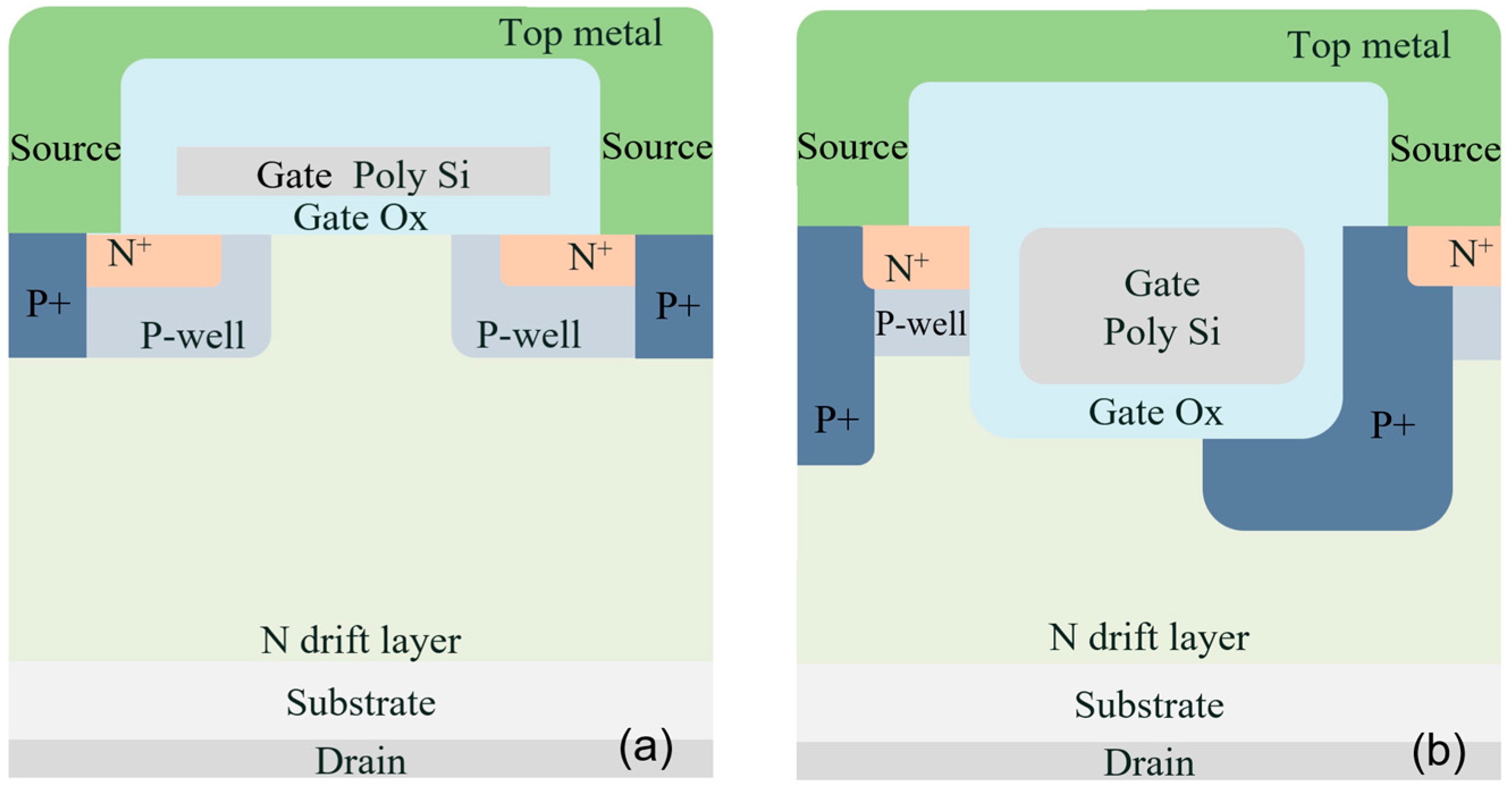
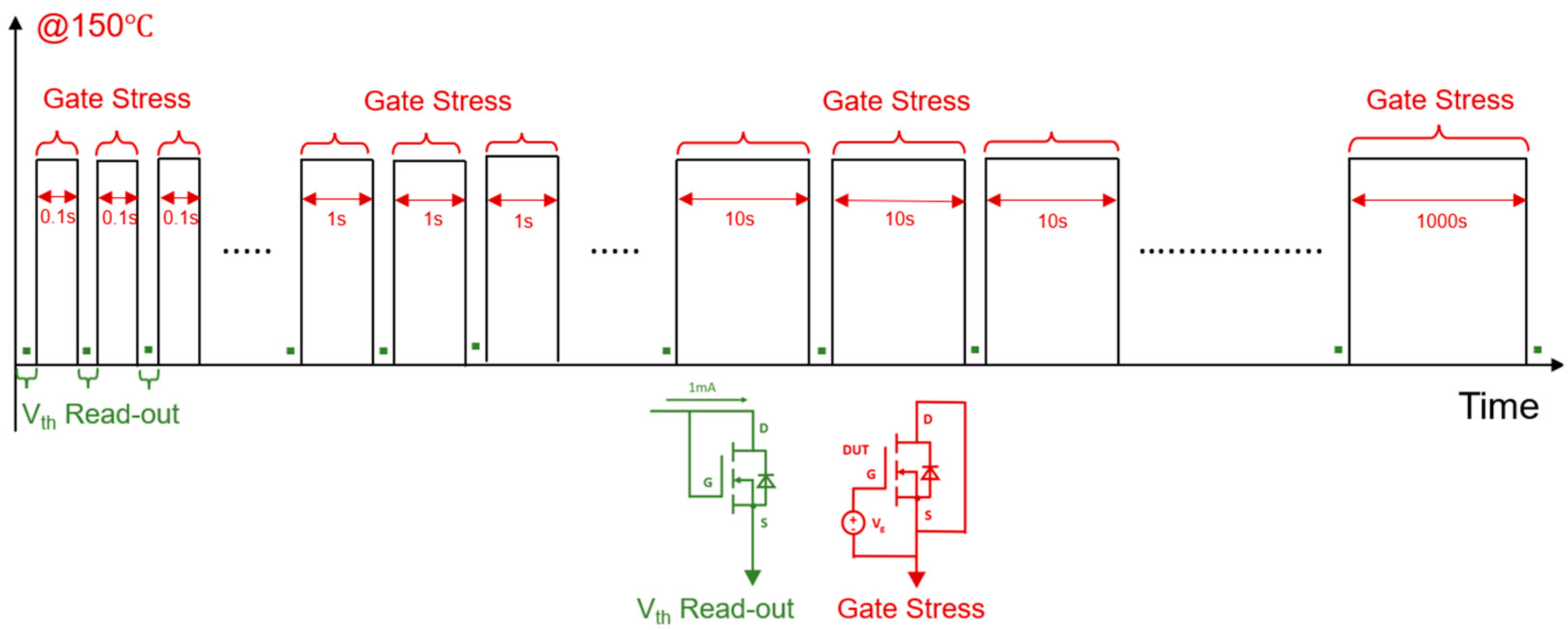
2. Experiment
3. Results
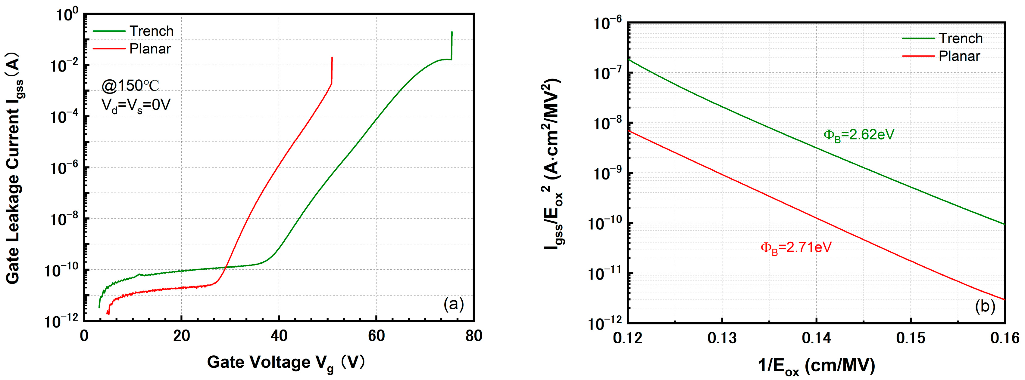
3.1. - Characteristic of Gate Oxide at 150 °C
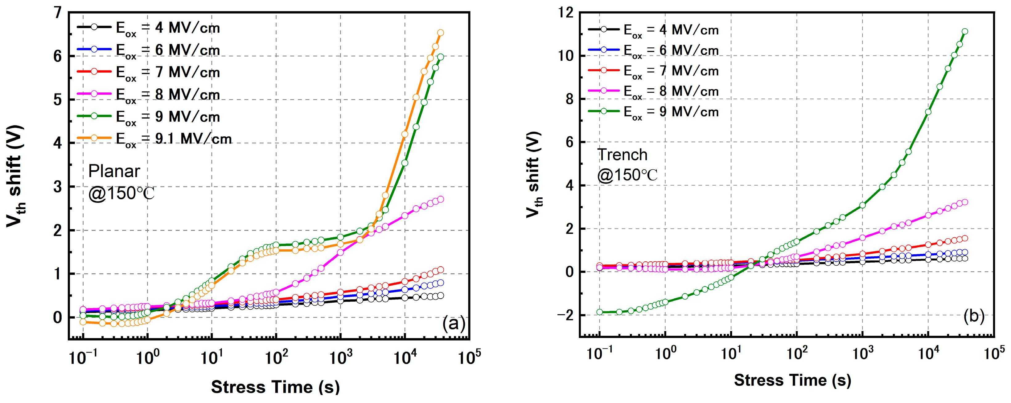
3.2. Influence of HTGB on Threshold Voltage
3.3. Influence of HTGB on Gate Leakage Current
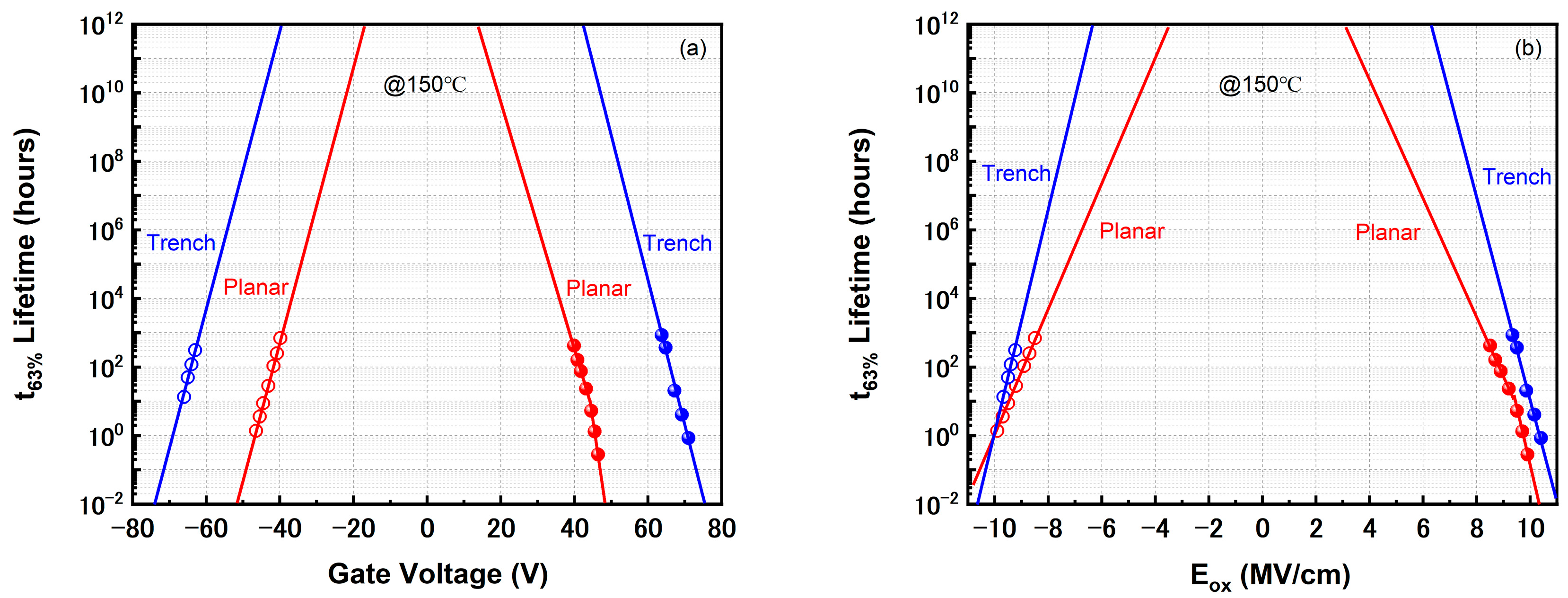
3.4. Constant-Voltage TDDB Test
4. Conclusions
Author Contributions
Funding
Data Availability Statement
Conflicts of Interest
References
- Zhu, S.; Shi, L.; Jin, M.; Qian, J.; Bhattacharya, M.; Rao Maddi, H.L.; White, M.H.; Agarwal, A.K.; Liu, T.; Shimbori, A.; et al. Reliability Comparison of Commercial Planar and Trench 4H-SiC Power MOSFETs. In Proceedings of the 2023 IEEE International Reliability Physics Symposium (IRPS), Monterey, CA, USA, 26–30 March 2023; IEEE: Piscataway, NJ, USA, 2023; pp. 1–5. [Google Scholar]
- Peters, D.; Siemieniec, R.; Aichinger, T.; Basler, T.; Esteve, R.; Bergner, W.; Kueck, D. Performance and ruggedness of 120 0V SiC—Trench—MOSFET. In Proceedings of the 2017 29th International Symposium on Power Semiconductor Devices and IC’s (ISPSD), Sapporo, Japan, 28 May–1 June 2017; pp. 239–242. [Google Scholar]
- Williams, R.K.; Darwish, M.N.; Blanchard, R.A.; Siemieniec, R.; Rutter, P.; Kawaguchi, Y. The Trench Power MOSFET: Part I—History, Technology, and Prospects. IEEE Trans. Electron Devices 2017, 64, 674–691. [Google Scholar] [CrossRef]
- Chaturvedi, M.; Dimitrijev, S.; Haasmann, D.; Moghadam, H.A.; Pande, P.; Jadli, U. Comparison of Commercial Planar and Trench SiC MOSFETs by Electrical Characterization of Performance-Degrading Near-Interface Traps. IEEE Trans. Electron Devices 2022, 69, 6225–6230. [Google Scholar] [CrossRef]
- Qian, J.; Shi, L.; Jin, M.; Bhattacharya, M.; Shimbori, A.; Yu, H.; Houshmand, S.; White, M.H.; Agarwal, A.K. An Investigation of Body Diode Reliability in Commercial 1.2 kV SiC Power MOSFETs with Planar and Trench Structures. Micromachines 2024, 15, 177. [Google Scholar] [CrossRef] [PubMed]
- Deng, X.; Zhu, H.; Li, X.; Tong, X.; Gao, S.; Wen, Y.; Bai, S.; Chen, W.; Zhou, K.; Zhang, B. Investigation and Failure Mode of Asymmetric and Double Trench SiC mosfets Under Avalanche Conditions. IEEE Trans. Power Electron. 2020, 35, 8524–8531. [Google Scholar] [CrossRef]
- Bhattacharya, M.; Jin, M.; Qian, J.; Shi, L.; Yu, H.; White, M.H.; Agarwal, A.K. The Effect of Cryogenic Temperature on Subthreshold Hysteresis of Commercial SiC Power MOSFETs. In Proceedings of the 2023 IEEE 10th Workshop on Wide Bandgap Power Devices & Applications (WiPDA), Charlotte, NC, USA, 4–6 December 2023; IEEE: Piscataway, NJ, USA, 2023; pp. 1–4. [Google Scholar]
- Senzaki, J.; Kojima, K.; Harada, S.; Kosugi, R.; Suzuki, S.; Suzuki, T.; Fukuda, K. Excellent effects of hydrogen postoxidation annealing on inversion channel mobility of 4H-SiC MOSFET fabricated on (11 2 0) face. IEEE Electron Device Lett. 2002, 23, 13–15. [Google Scholar] [CrossRef]
- Chung, G.Y.; Tin, C.C.; Williams, J.R.; McDonald, K.; Chanana, R.K.; Weller, R.A.; Pantelides, S.T.; Feldman, L.C.; Holland, O.W.; Das, M.K.; et al. Improved inversion channel mobility for 4H-SiC MOSFETs following high temperature anneals in nitric oxide. IEEE Electron Device Lett. 2001, 22, 176–178. [Google Scholar] [CrossRef]
- Jia, Y.; Lv, H.; Song, Q.; Tang, X.; Xiao, L.; Wang, L.; Tang, G.; Zhang, Y.; Zhang, Y. Influence of oxidation temperature on the interfacial properties of n-type 4H-SiC MOS capacitors. Appl. Surf. Sci. 2017, 397, 175–182. [Google Scholar] [CrossRef]
- Lu, C.-Y.; Cooper, J.A.; Tsuji, T.; Chung, G.; Williams, J.R.; McDonald, K.; Feldman, L.C. Effect of process variations and ambient temperature on electron mobility at the SiO/sub 2//4H-SiC interface. IEEE Trans. Electron Devices 2003, 50, 1582–1588. [Google Scholar] [CrossRef]
- Wang, J.; Jiang, X. Review and analysis of SiC MOSFETs’ ruggedness and reliability. IET Power Electron. 2020, 13, 445–455. [Google Scholar] [CrossRef]
- Maddi, H.L.R.; Yu, S.; Zhu, S.; Liu, T.; Shi, L.; Kang, M.; Xing, D.; Nayak, S.; White, M.H.; Agarwal, A.K. The Road to a Robust and Affordable SiC Power MOSFET Technology. Energies 2021, 14, 8283. [Google Scholar] [CrossRef]
- Green, R.; Lelis, A.; Habersat, D. Threshold-voltage bias-temperature instability in commercially-available SiC MOSFETs. Jpn. J. Appl. Phys. 2016, 55, 04EA03. [Google Scholar] [CrossRef]
- Noguchi, M.; Koyama, A.; Iwamatsu, T.; Amishiro, H.; Watanabe, H.; Miura, N. Gate Oxide Instability and Lifetime in SiC MOSFETs under a Wide Range of Positive Electric Field Stress. In Proceedings of the 2020 IEEE International Electron Devices Meeting (IEDM), San Francisco, CA, USA, 12–18 December 2020; IEEE: Piscataway, NJ, USA, 2020; pp. 23.4.1–23.4.4. [Google Scholar]
- Lelis, A.J.; Green, R.; Habersat, D.B.; El, M. Basic Mechanisms of Threshold-Voltage Instability and Implications for Reliability Testing of SiC MOSFETs. IEEE Trans. Electron Devices 2015, 62, 316–323. [Google Scholar] [CrossRef]
- Boldyrjew-Mast, R.; Thiele, S.; Schöttler, N.; Basler, T.; Lutz, J. Gate Oxide Reliability of 1.2 kV and 6.5 kV SiC MOSFETs under Stair-Shaped Increase of Positive and Negative Gate Bias. In Proceedings of the 2021 33rd International Symposium on Power Semiconductor Devices and ICs (ISPSD), Nagoya, Japan, 30 May–3 June 2021; IEEE: Piscataway, NJ, USA, 2021; pp. 243–246. [Google Scholar]
- Yen, C.-T.; Hung, C.-C.; Hung, H.-T.; Lee, C.-Y.; Lee, L.-S.; Huang, Y.-F.; Hsu, F.-J. Negative bias temperature instability of SiC MOSFET induced by interface trap assisted hole trapping. Appl. Phys. Lett. 2016, 108, 012106. [Google Scholar] [CrossRef]
- Peters, D.; Aichinger, T.; Basler, T.; Rescher, G.; Puschkarsky, K.; Reisinger, H. Investigation of threshold voltage stability of SiC MOSFETs. In Proceedings of the 2018 IEEE 30th International Symposium on Power Semiconductor Devices and ICs (ISPSD), Chicago, IL, USA, 13–17 May 2018; IEEE: Piscataway, NJ, USA, 2018; pp. 40–43. [Google Scholar]
- Maas, S.; Reisinger, H.; Aichinger, T.; Rescher, G. Influence of high-voltage gate-oxide pulses on the BTI behavior of SiC MOSFETs. In Proceedings of the 2020 IEEE International Reliability Physics Symposium (IRPS), Dallas, TX, USA, 28 April–30 May 2020; IEEE: Piscataway, NJ, USA, 2020; pp. 1–6. [Google Scholar]
- Yu, S.; Liu, T.; Zhu, S.; Xing, D.; Salemi, A.; Kang, M.; Booth, K.; White, M.H.; Agarwal, A.K. Threshold Voltage Instability of Commercial 1.2 kV SiC Power MOSFETs. In Proceedings of the 2020 IEEE International Reliability Physics Symposium (IRPS), Dallas, TX, USA, 28 April–30 May 2020; IEEE: Piscataway, NJ, USA, 2020; pp. 1–5. [Google Scholar]
- Shi, L.; Qian, J.; Jin, M.; Bhattacharya, M.; Yu, H.; White, M.H.; Agarwal, A.K.; Shimbori, A.; Xu, Z. An Effective Screening Technique for Early Oxide Failure in SiC Power MOSFETs. In Proceedings of the 2023 IEEE 10th Workshop on Wide Bandgap Power Devices & Applications (WiPDA), Charlotte, NC, USA, 4–6 December 2023; IEEE: Piscataway, NJ, USA, 2023; pp. 1–4. [Google Scholar]
- Zhu, S.; Liu, T.; White, M.H.; Agarwal, A.K.; Salemi, A.; Sheridan, D. Investigation of Gate Leakage Current Behavior for Commercial 1.2 kV 4H-SiC Power MOSFETs. In Proceedings of the 2021 IEEE International Reliability Physics Symposium (IRPS), Monterey, CA, USA, 21–25 March 2021; IEEE: Piscataway, NJ, USA, 2021; pp. 1–7. [Google Scholar]
- Qian, J.; Shi, L.; Jin, M.; Bhattacharya, M.; Yu, H.; White, M.H.; Agarwal, A.K.; Shimbori, A.; Liu, T.; Zhu, S. Investigation of the Electron Trapping in Commercial Thick Silicon Dioxides Thermally Grown on 4H-SiC under the Constant Current Stress. In Proceedings of the 2024 IEEE International Reliability Physics Symposium (IRPS), Grapevine, TX, USA, 14–18 April 2024; IEEE: Piscataway, NJ, USA, 2024; pp. 1–6. [Google Scholar]
- McPherson, J.W.; Mogul, H.C. Underlying physics of the thermochemical E model in describing low-field time-dependent dielectric breakdown in SiO2 thin films. J. Appl. Phys. 1998, 84, 1513–1523. [Google Scholar] [CrossRef]
- Shi, L.; Qian, J.; Jin, M.; Bhattacharya, M.; Yu, H.; Shimbori, A.; White, M.H.; Agarwal, A.K. Investigation on gate oxide reliability under gate bias screening for commercial SiC planar and trench MOSFETs. Mater. Sci. Semicond. Process. 2024, 174, 108194. [Google Scholar] [CrossRef]
- Liu, T.; Zhu, S.; White, M.H.; Salemi, A.; Sheridan, D.; Agarwal, A.K. Time-Dependent Dielectric Breakdown of Commercial 1.2 kV 4H-SiC Power MOSFETs. IEEE J. Electron Devices Soc. 2021, 9, 633–639. [Google Scholar] [CrossRef]
- Lin, W.-C.; Yu, W.-C.; Chen, B.-R.; Hsiao, Y.-S.; Huang, Z.-H.; Hung, C.-L.; Hsiao, Y.-K.; Yeh, N.-J.; Kuo, H.-C.; Tu, C.-C.; et al. Investigation of the time dependent gate dielectric stability in SiC MOSFETs with planar and trench gate structures. Microelectron. Reliab. 2023, 150, 115141. [Google Scholar] [CrossRef]
- Fiorenza, P.; Frazzetto, A.; Guarnera, A.; Saggio, M.; Roccaforte, F. Fowler-Nordheim tunneling at SiO2/4H-SiC interfaces in metal-oxide-semiconductor field effect transistors. Appl. Phys. Lett. 2014, 105, 142108. [Google Scholar] [CrossRef]
- Agarwal, A.K.; Seshadri, S.; Rowland, L.B. Temperature dependence of Fowler-Nordheim current in 6H- and 4H-SiC MOS capacitors. IEEE Electron Device Lett. 1997, 18, 592–594. [Google Scholar] [CrossRef]
- Fiorenza, P.; La Magna, A.; Vivona, M.; Roccaforte, F. Near interface traps in SiO2/4H-SiC metal-oxide-semiconductor field effect transistors monitored by temperature dependent gate current transient measurements. Appl. Phys. Lett. 2016, 109, 012102. [Google Scholar] [CrossRef]
- Ma, Z.J.; Lai, P.T.; Liu, Z.H.; Fleischer, S.; Cheng, Y.C. Tunneling-injection-induced turnaround behavior of threshold voltage in thermally nitrided oxide n-channel metal-oxide-semiconductor field-effect transistors. J. Appl. Phys. 1990, 68, 6299–6303. [Google Scholar] [CrossRef]
- DiMaria, D.J.; Cartier, E.; Buchanan, D.A. Anode hole injection and trapping in silicon dioxide. J. Appl. Phys. 1996, 80, 304–317. [Google Scholar] [CrossRef]
- Shi, L.; Liu, T.; Zhu, S.; Qian, J.; Jin, M.; Maddi, H.L.R.; White, M.H.; Agarwal, A.K. Effects of Oxide Electric Field Stress on the Gate Oxide Reliability of Commercial SiC Power MOSFETs. In Proceedings of the 2022 IEEE 9th Workshop on Wide Bandgap Power Devices & Applications (WiPDA), Redondo Beach, CA, USA, 7–9 November 2022; IEEE: Piscataway, NJ, USA, 2022; pp. 45–48. [Google Scholar]
- Shi, L.; Zhu, S.; Qian, J.; Jin, M.; Bhattacharya, M.; White, M.H.; Agarwal, A.K.; Shimbori, A.; Liu, T. Investigation of different screening methods on threshold voltage and gate oxide lifetime of SiC Power MOSFETs. In Proceedings of the 2023 IEEE International Reliability Physics Symposium (IRPS), Monterey, CA, USA, 26–30 March 2023; IEEE: Piscataway, NJ, USA, 2023; pp. 1–7. [Google Scholar]
- Rescher, G.; Pobegen, G.; Aichinger, T.; Grasser, T. On the subthreshold drain current sweep hysteresis of 4H-SiC nMOSFETs. In Proceedings of the 2016 IEEE International Electron Devices Meeting (IEDM), San Francisco, CA, USA, 3–7 December 2016; IEEE: Piscataway, NJ, USA, 2016; pp. 10.8.1–10.8.4. [Google Scholar]
- Noguchi, M.; Koyama, A.; Iwamatsu, T.; Watanabe, H.; Miura, N. Gate Oxide Instability against a Wide Range of Negative Electric Field Stress of SiC MOSFETs. In Proceedings of the 2021 IEEE International Electron Devices Meeting (IEDM), San Francisco, CA, USA, 11–16 December 2021; IEEE: Piscataway, NJ, USA, 2021; pp. 36.3.1–36.3.4. [Google Scholar]
- Shen, Y.; He, Z.; Shi, Y.; Niu, H.; Chen, Y.; Liu, C.; Chen, Y.; Cai, Z.; Lu, G.; Dai, X. Time-Dependent Degradation Mechanism of 1.2 kV SiC MOSFET Under Long-Term High-Temperature Gate Bias Stress. IEEE Trans. Electron Devices. 2023, 70, 1162–1167. [Google Scholar] [CrossRef]
- Shi, L.; Qian, J.; Jin, M.; Bhattacharya, M.; Yu, H.; White, M.H.; Agarwal, A.K.; Shimbori, A. Evaluation of Burn-in Technique on Gate Oxide Reliability in Commercial SiC MOSFETs. In Proceedings of the 2024 IEEE International Reliability Physics Symposium (IRPS), Grapevine, TX, USA, 14–18 April 2024; IEEE: Piscataway, NJ, USA, 2024; pp. 1–6. [Google Scholar]
- Ganguly, S.; Lichtenwalner, D.J.; Isaacson, C.; Gajewski, D.A.; Steinmann, P.; Foarde, R.; Hull, B.; Ryu, S.-H.; Allen, S.; Palmour, J.W. Negative Gate Bias TDDB evaluation of n-Channel SiC Vertical Power MOSFETs. In Proceedings of the 2022 IEEE International Reliability Physics Symposium (IRPS), Dallas, TX, USA, 27–31 March 2022; IEEE: Piscataway, NJ, USA, 2022; pp. 8B.1-1–8B.1-6. [Google Scholar]
- Moens, P.; Franchi, J.; Lettens, J.; Schepper, L.D.; Domeij, M.; Allerstam, F. A Charge-to-Breakdown (QBD) Approach to SiC Gate Oxide Lifetime Extraction and Modeling. In Proceedings of the 2020 32nd International Symposium on Power Semiconductor Devices and ICs (ISPSD), Vienna, Austria, 13–18 September 2020; IEEE: Piscataway, NJ, USA, 2020; pp. 78–81. [Google Scholar]
- Zhu, S.; Liu, T.; Shi, L.; Jin, M.; Maddi, H.L.R.; White, M.H.; Agarwal, A.K. Comparison of Gate Oxide Lifetime Predictions with Charge-to-Breakdown Approach and Constant-Voltage TDDB on SiC Power MOSFET. In Proceedings of the 2021 IEEE 8th Workshop on Wide Bandgap Power Devices and Applications (WiPDA), Redondo Beach, CA, USA, 7–11 November 2021; IEEE: Piscataway, NJ, USA, 2021; pp. 1–4. [Google Scholar]
- Qian, J.; Shi, L.; Jin, M.; Bhattacharya, M.; Shimbori, A.; Yu, H.; Houshmand, S.; White, M.H.; Agarwal, A.K. Modeling of Charge-to-Breakdown with an Electron Trapping Model for Analysis of Thermal Gate Oxide Failure Mechanism in SiC Power MOSFETs. Materials 2024, 17, 1455. [Google Scholar] [CrossRef]
- Qian, J.; Shi, L.; Jin, M.; Bhattacharya, M.; Yu, H.; White, M.H.; Agarwal, A.K.; Shimbori, A.; Xu, Z. Investigation of the Constant Current Stress for Charge-to-breakdown Extraction in Commercial SiC Power MOSFETs. In Proceedings of the 2023 IEEE 10th Workshop on Wide Bandgap Power Devices & Applications (WiPDA), Charlotte, NC, USA, 4–6 December 2023; IEEE: Piscataway, NJ, USA, 2023; pp. 1–4. [Google Scholar]


| Device Parameter | SiC Planar MOSFET | SiC Trench MOSFET |
|---|---|---|
| Package | TO247-3 | TO247-3 |
| Gate structure | Planar | Asymmetric trench |
| On-resistance (mΩ) | 280 | 220 |
| Threshold voltage at RT (V) | ~6 | ~7 |
| TDDB | SiC Planar MOSFETs | SiC Trench MOSFETs | ||||
|---|---|---|---|---|---|---|
| Positive-TDDB | 46.43 V | 9.9 MV/cm | 0.28 h | 63.7 V | 9.34 MV/cm | 850 h |
| 45.49 V | 9.7 MV/cm | 1.31 h | 64.8 V | 9.5 MV/cm | 369 h | |
| 44.55 V | 9.5 MV/cm | 5.3 h | 67.2V | 9.85 MV/cm | 20.31 h | |
| 43.15 V | 9.2 MV/cm | 23.4 h | 69.2 V | 10.15 MV/cm | 4.05 h | |
| 41.74 V | 8.9 MV/cm | 75.2 h | 71 V | 10.4 MV/cm | 0.85 h | |
| 40.80 V | 8.7 MV/cm | 159.5 h | ||||
| 39.87 V | 8.5 MV/cm | 419.5 h | ||||
| Negative-TDDB | −46.43 V | −9.9 MV/cm | 1.38 h | −63 V | −9.23 MV/cm | 307.6 h |
| −45.49 V | −9.7 MV/cm | 3.6 h | −64 V | −9.4 MV/cm | 117.5 h | |
| −44.55 V | −9.5 MV/cm | 8.7 h | −65 V | −9.5 MV/cm | 49.45 h | |
| −43.15 V | −9.2 MV/cm | 28 h | −66 V | −9.67 MV/cm | 13.3 h | |
| −41.74 V | −8.9 MV/cm | 106.7 h | ||||
| −40.80 V | −8.7 MV/cm | 248.4 h | ||||
| −39.87 V | −8.5 MV/cm | 692 h | ||||
Disclaimer/Publisher’s Note: The statements, opinions and data contained in all publications are solely those of the individual author(s) and contributor(s) and not of MDPI and/or the editor(s). MDPI and/or the editor(s) disclaim responsibility for any injury to people or property resulting from any ideas, methods, instructions or products referred to in the content. |
© 2024 by the authors. Licensee MDPI, Basel, Switzerland. This article is an open access article distributed under the terms and conditions of the Creative Commons Attribution (CC BY) license (https://creativecommons.org/licenses/by/4.0/).
Share and Cite
Shi, L.; Qian, J.; Jin, M.; Bhattacharya, M.; Houshmand, S.; Yu, H.; Shimbori, A.; White, M.H.; Agarwal, A.K. Gate Oxide Reliability in Silicon Carbide Planar and Trench Metal-Oxide-Semiconductor Field-Effect Transistors Under Positive and Negative Electric Field Stress. Electronics 2024, 13, 4516. https://doi.org/10.3390/electronics13224516
Shi L, Qian J, Jin M, Bhattacharya M, Houshmand S, Yu H, Shimbori A, White MH, Agarwal AK. Gate Oxide Reliability in Silicon Carbide Planar and Trench Metal-Oxide-Semiconductor Field-Effect Transistors Under Positive and Negative Electric Field Stress. Electronics. 2024; 13(22):4516. https://doi.org/10.3390/electronics13224516
Chicago/Turabian StyleShi, Limeng, Jiashu Qian, Michael Jin, Monikuntala Bhattacharya, Shiva Houshmand, Hengyu Yu, Atsushi Shimbori, Marvin H. White, and Anant K. Agarwal. 2024. "Gate Oxide Reliability in Silicon Carbide Planar and Trench Metal-Oxide-Semiconductor Field-Effect Transistors Under Positive and Negative Electric Field Stress" Electronics 13, no. 22: 4516. https://doi.org/10.3390/electronics13224516
APA StyleShi, L., Qian, J., Jin, M., Bhattacharya, M., Houshmand, S., Yu, H., Shimbori, A., White, M. H., & Agarwal, A. K. (2024). Gate Oxide Reliability in Silicon Carbide Planar and Trench Metal-Oxide-Semiconductor Field-Effect Transistors Under Positive and Negative Electric Field Stress. Electronics, 13(22), 4516. https://doi.org/10.3390/electronics13224516