

Design and Implementation of 3 kW All-SiC Current Source Inverter


Abstract
1. Introduction
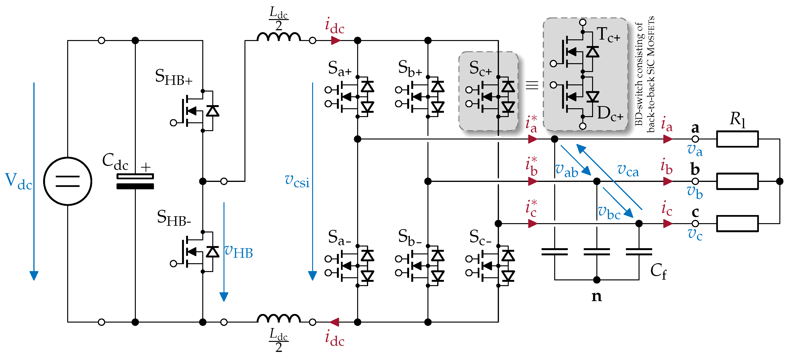
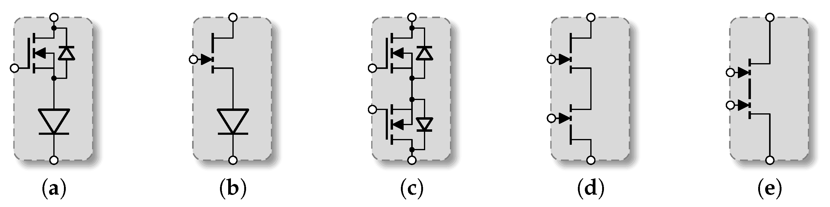
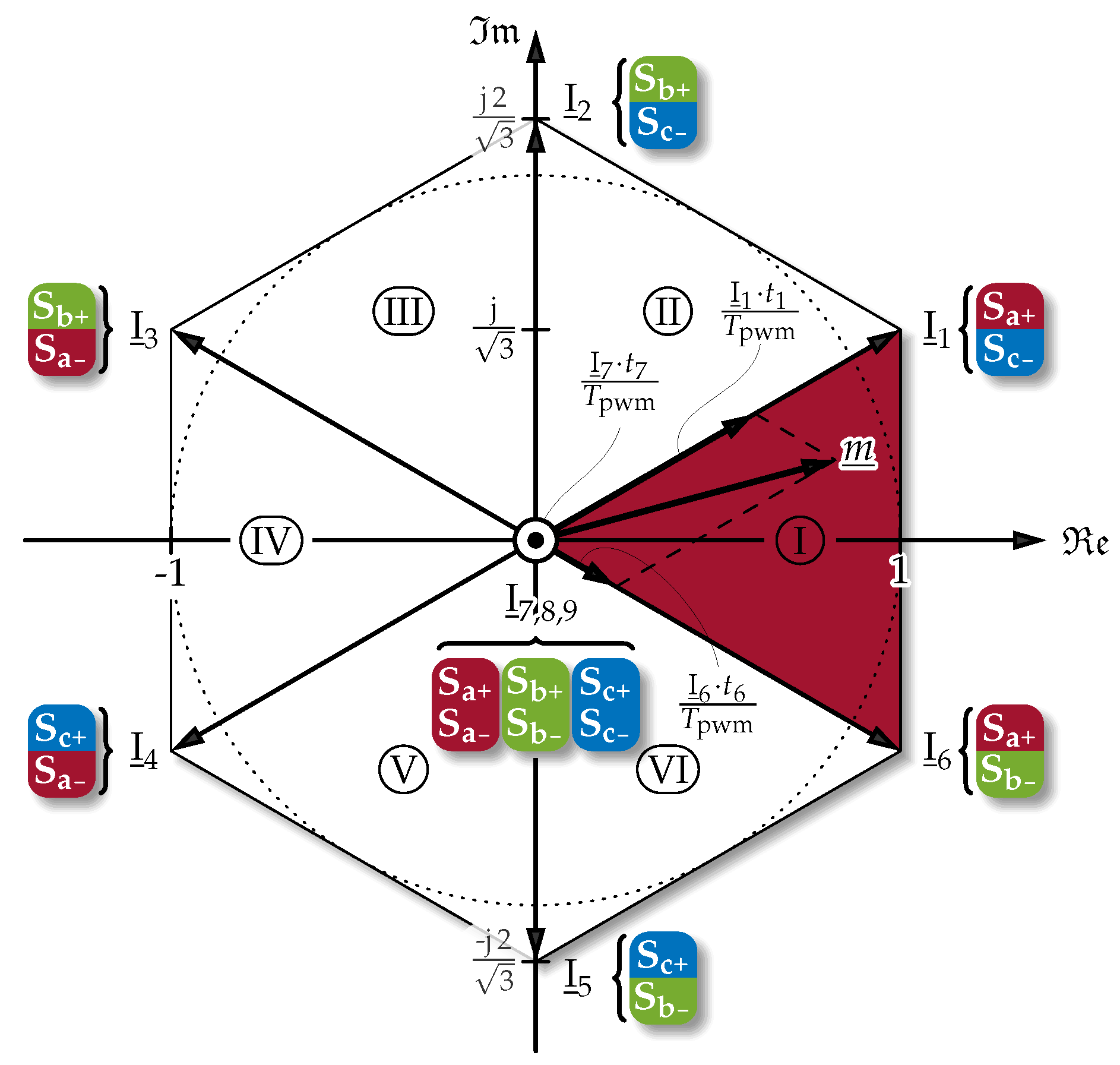
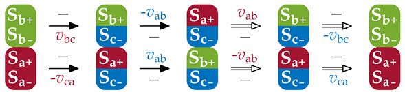
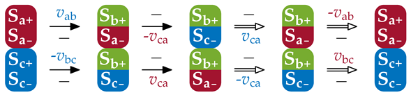
2. Basic Operating Principle of CSI
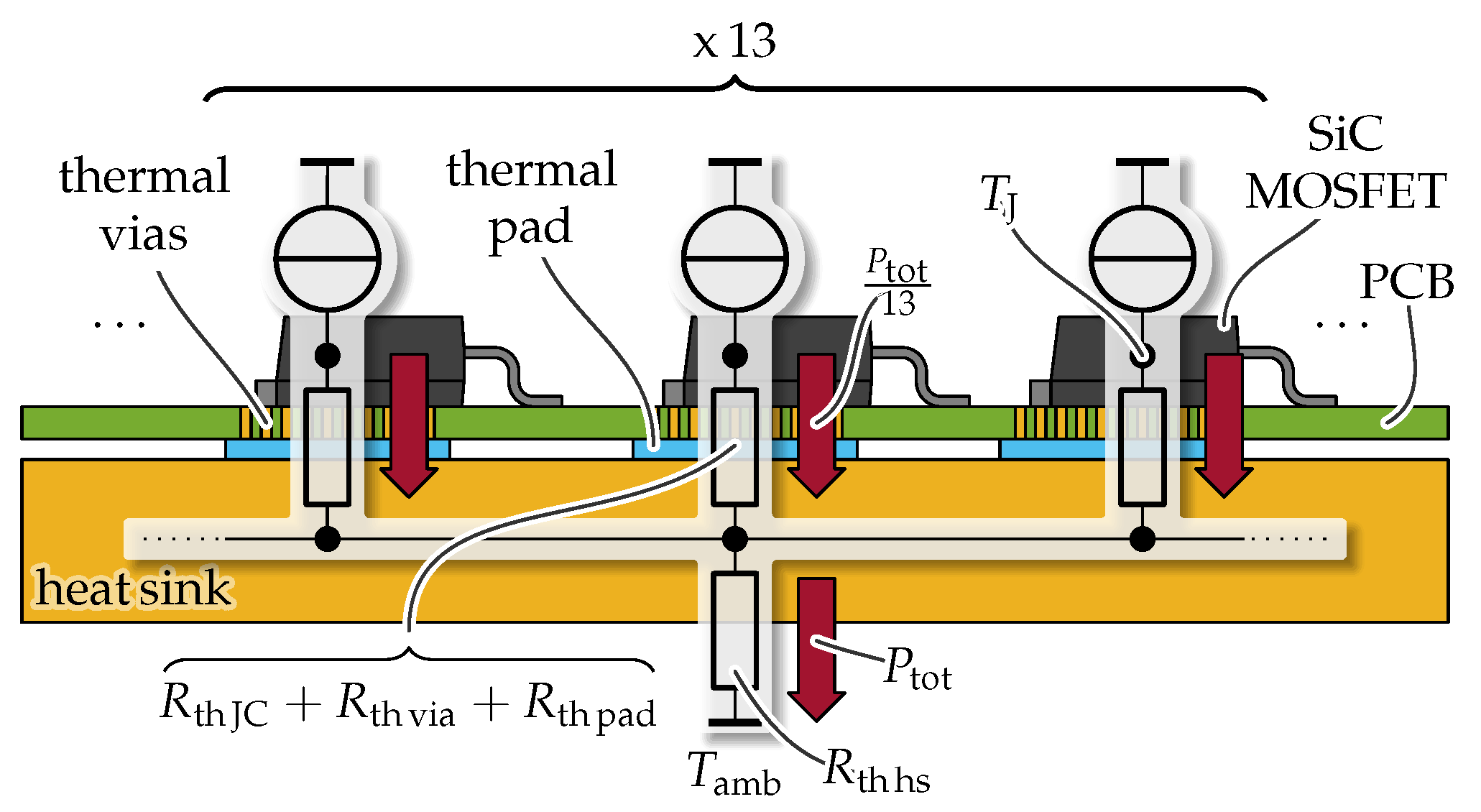
3. Power Semiconductor Losses
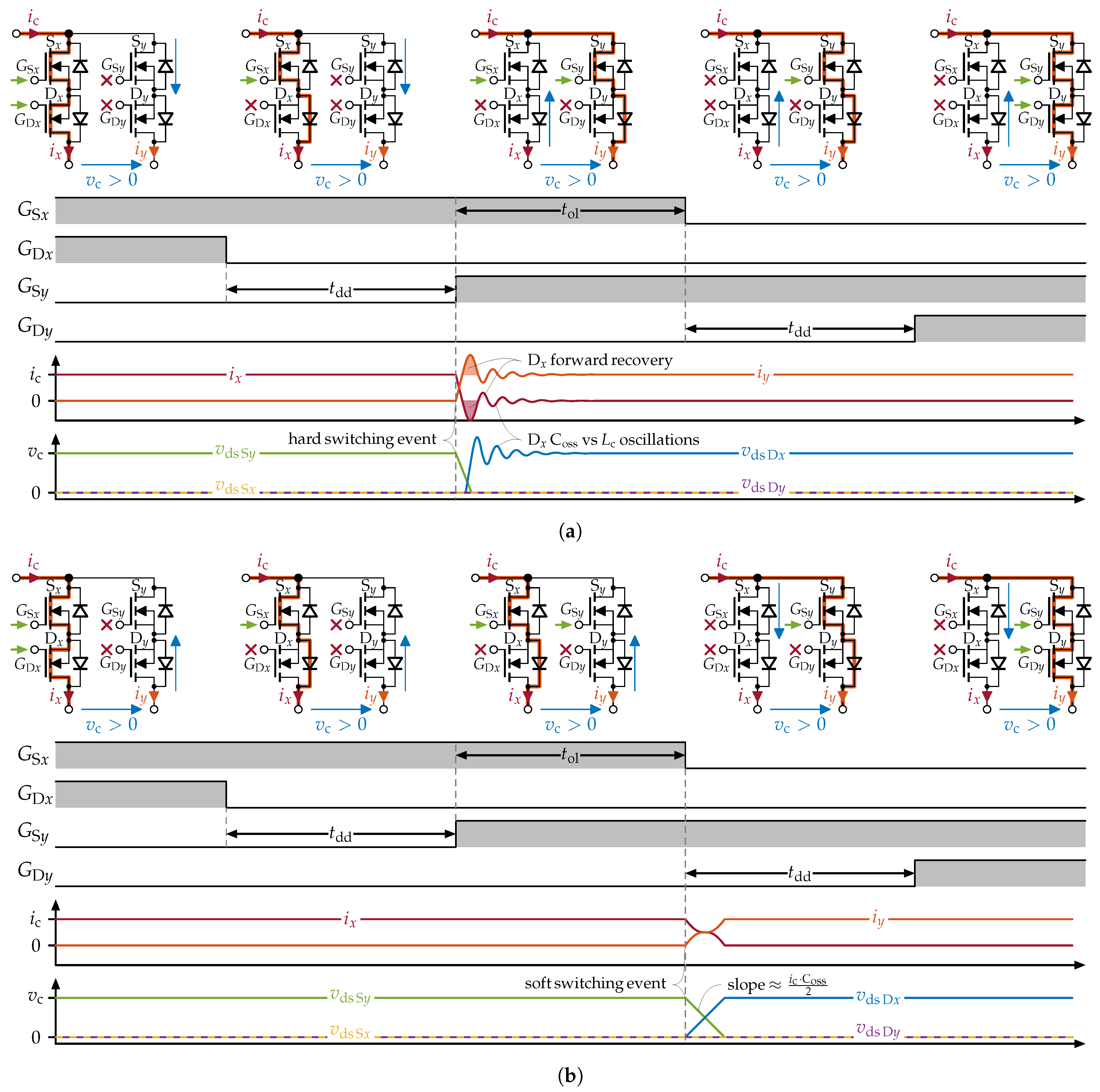
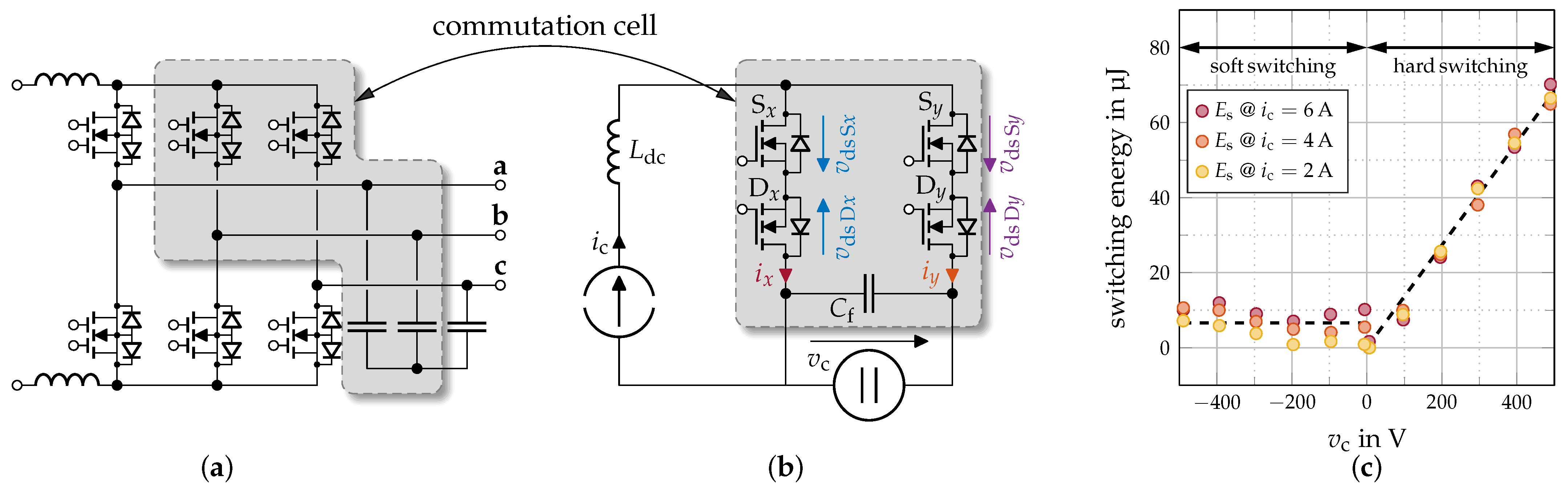
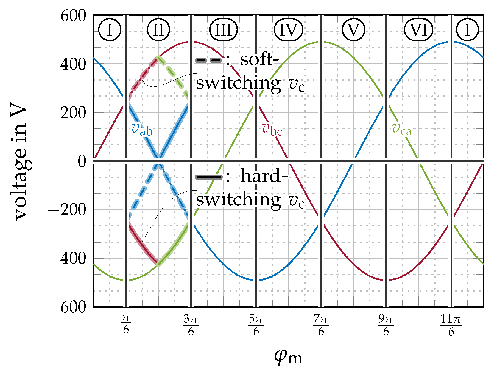
3.1. Switching Losses
3.2. Conduction Losses
4. Design of the Passive Components
4.1. Design of the Filter Capacitors

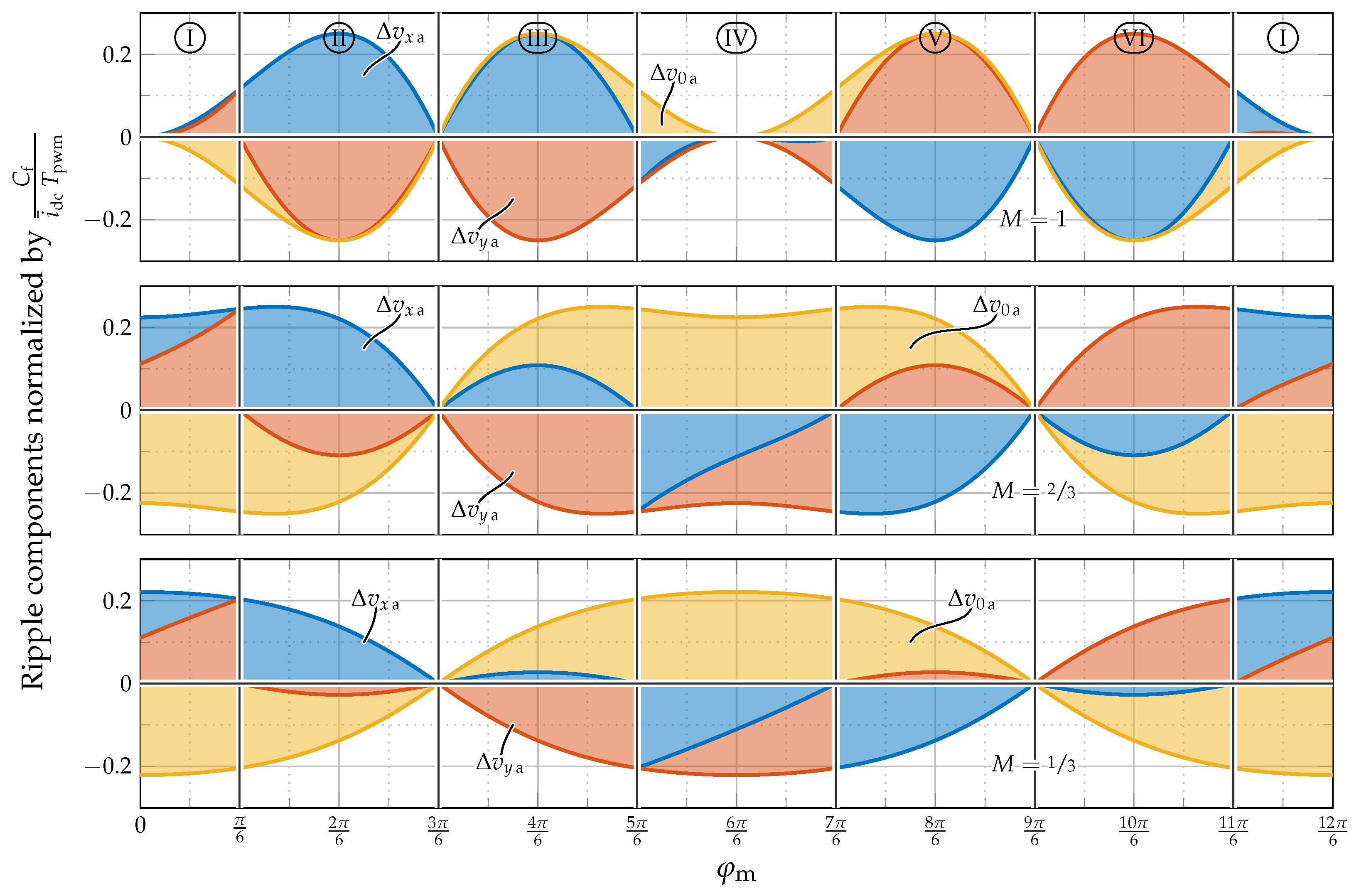
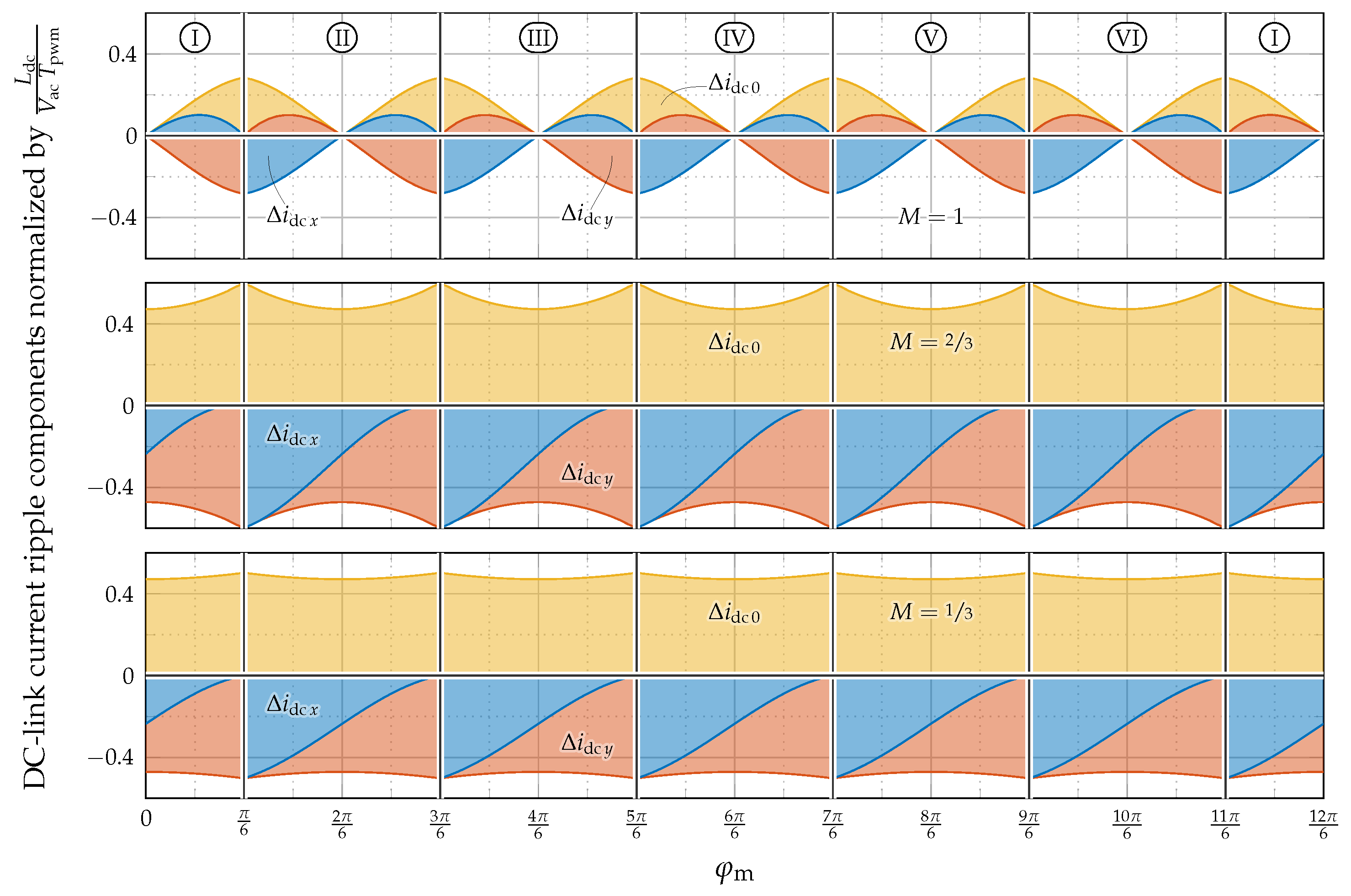
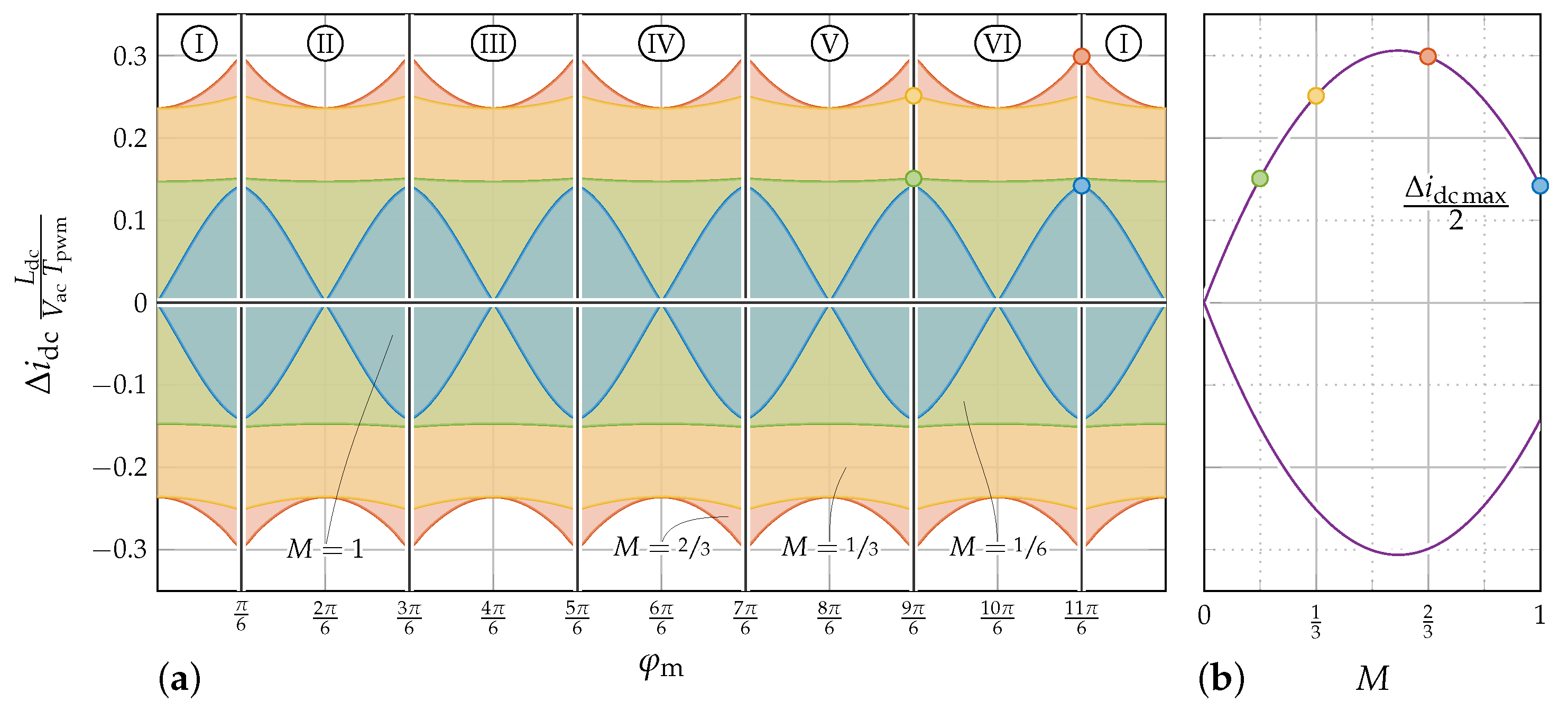
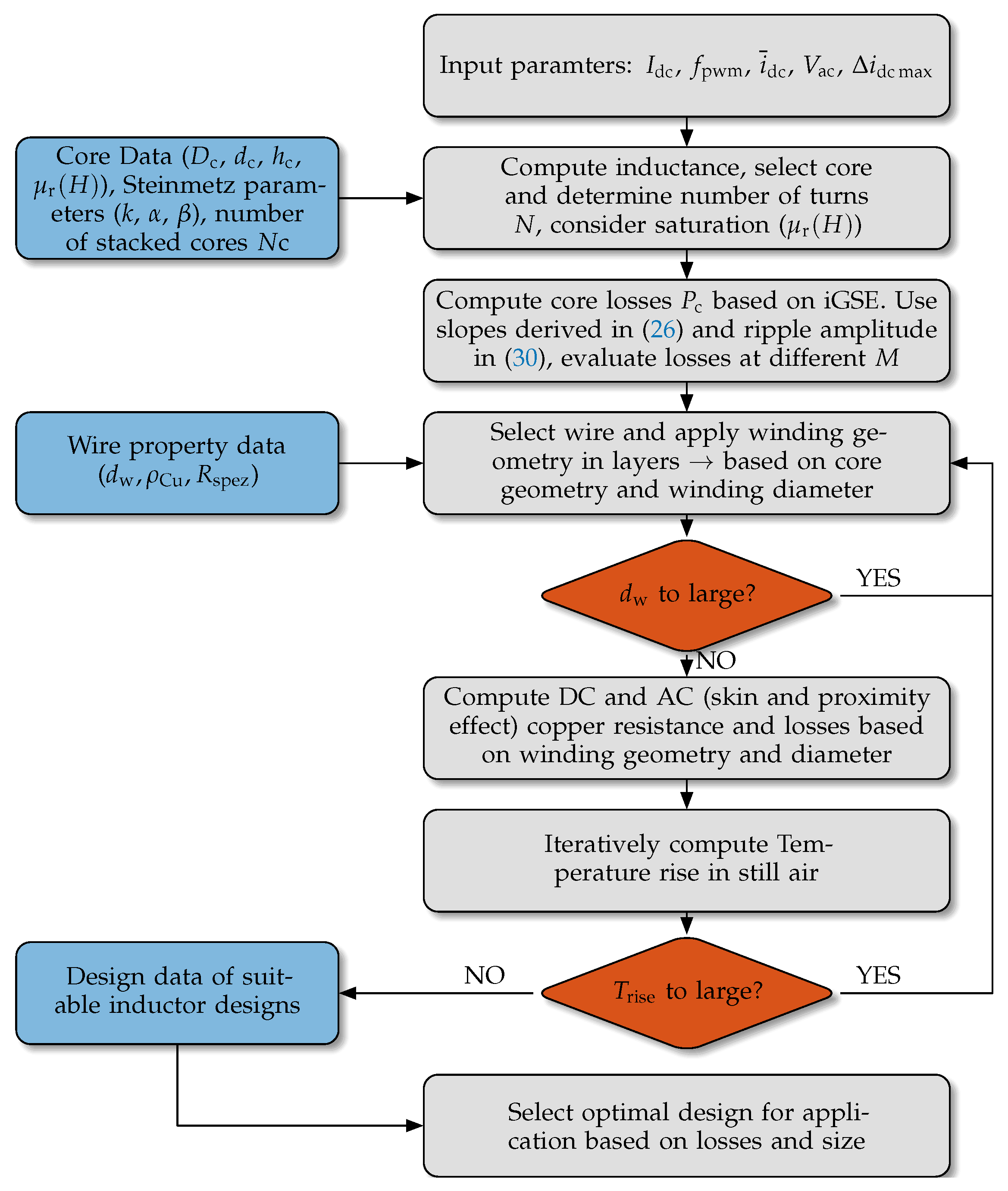
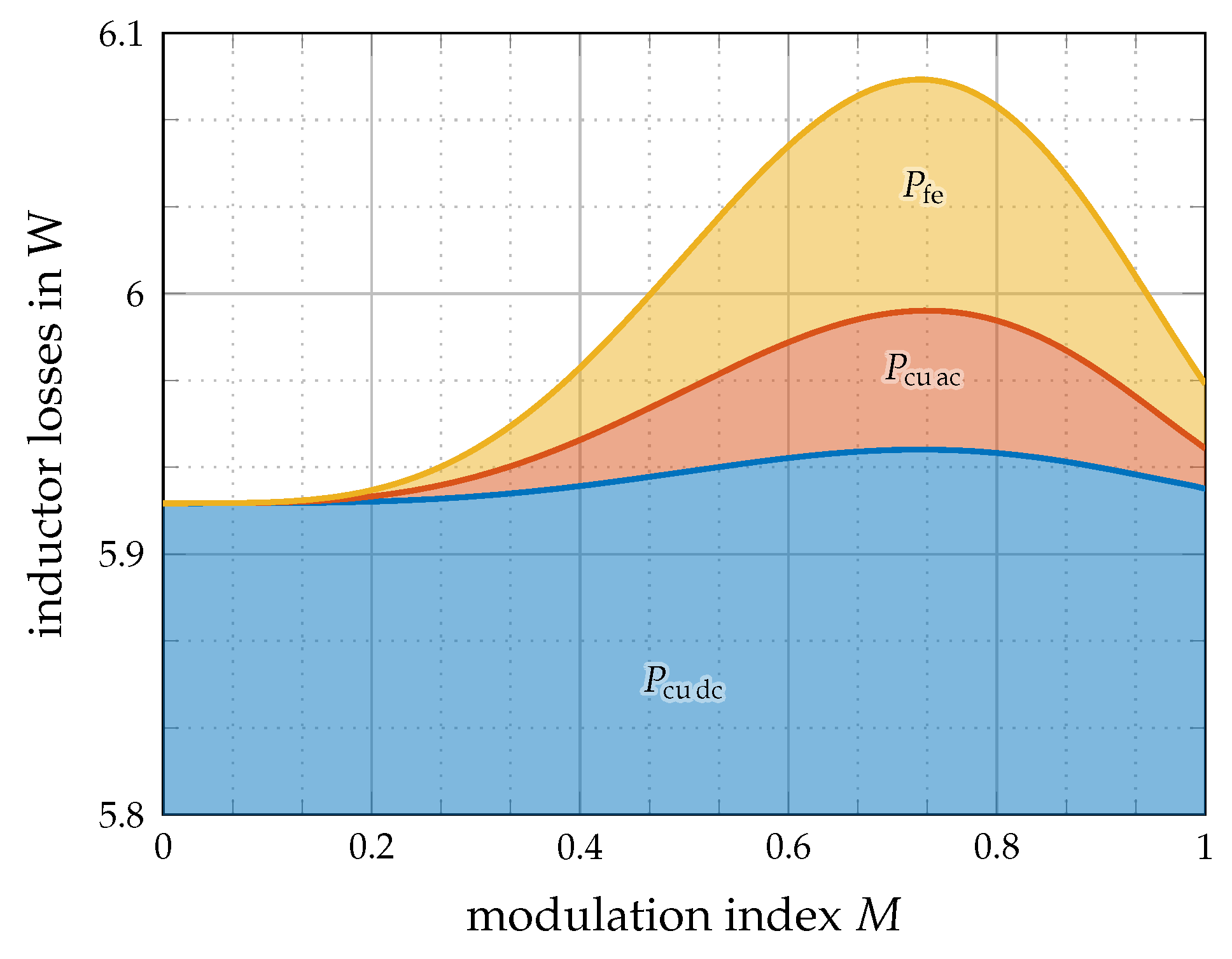
4.2. DC-Link Current Ripple—Design of DC-Link Inductor
- The inverter is supplied by a controlled DC voltage that maintains a constant average DC-link current (excluding the buck stage in the analysis).
- The load is symmetric and the filter capacitors are large enough to minimize voltage ripple, resulting in a purely three-phase sinusoidal output voltage system. This system can be phase-shifted to represent non-unity power factors.
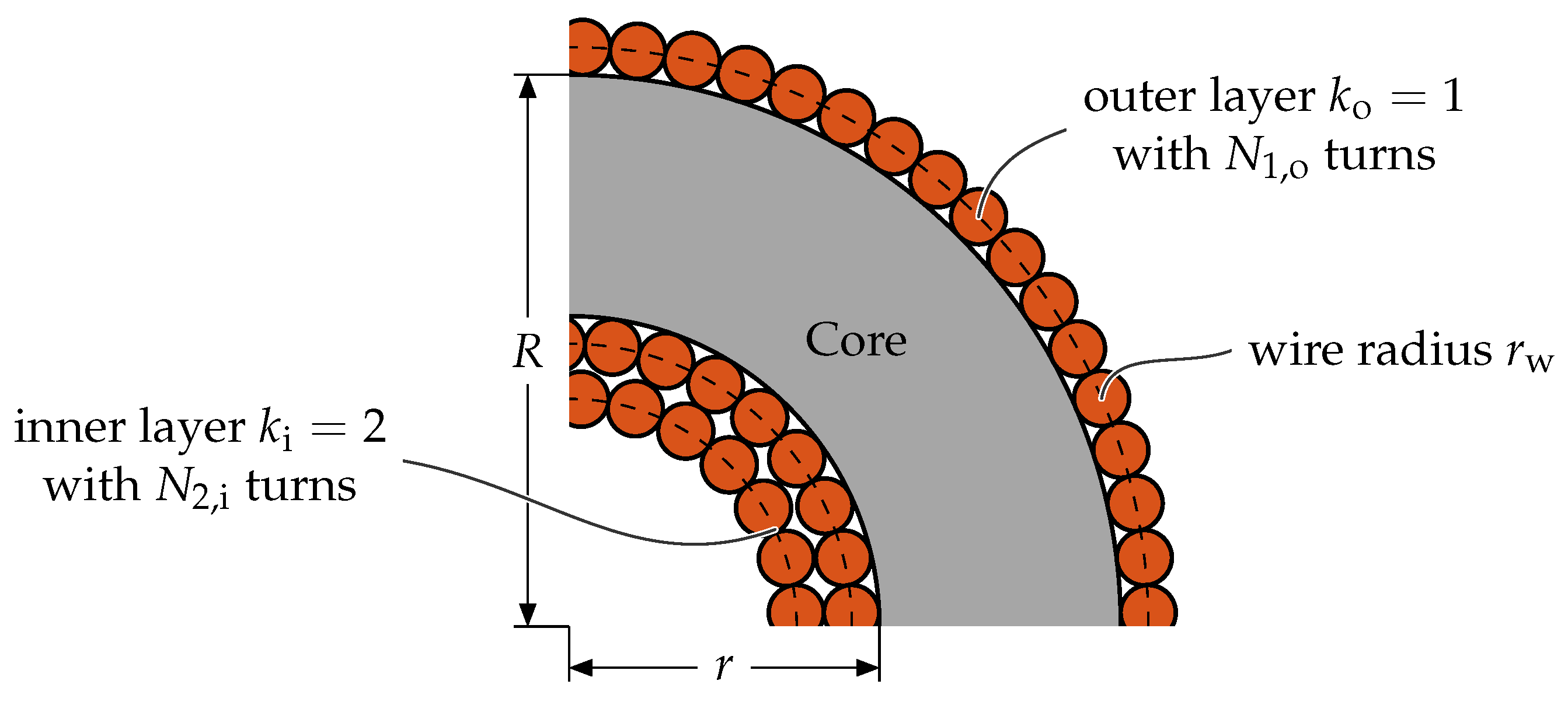
Design of the Inductor
- …skin depth
- …porosity factor
- …wire diameter
- n…harmonic order
- …PWM frequency (fundamental frequency of waveform)
- …relative conductivity of copper (0.01786 )
- t…distance between two adjacent conductors (here, was assumed)
5. Total Converter Losses
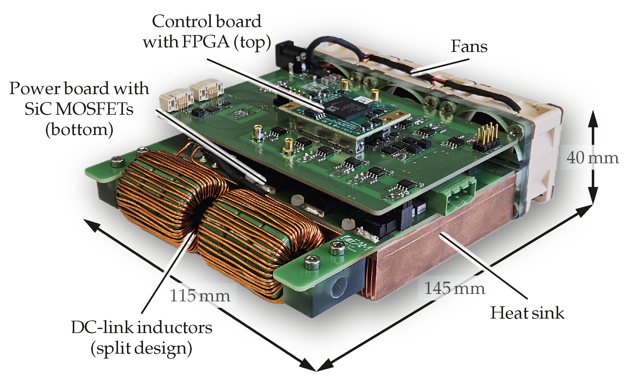
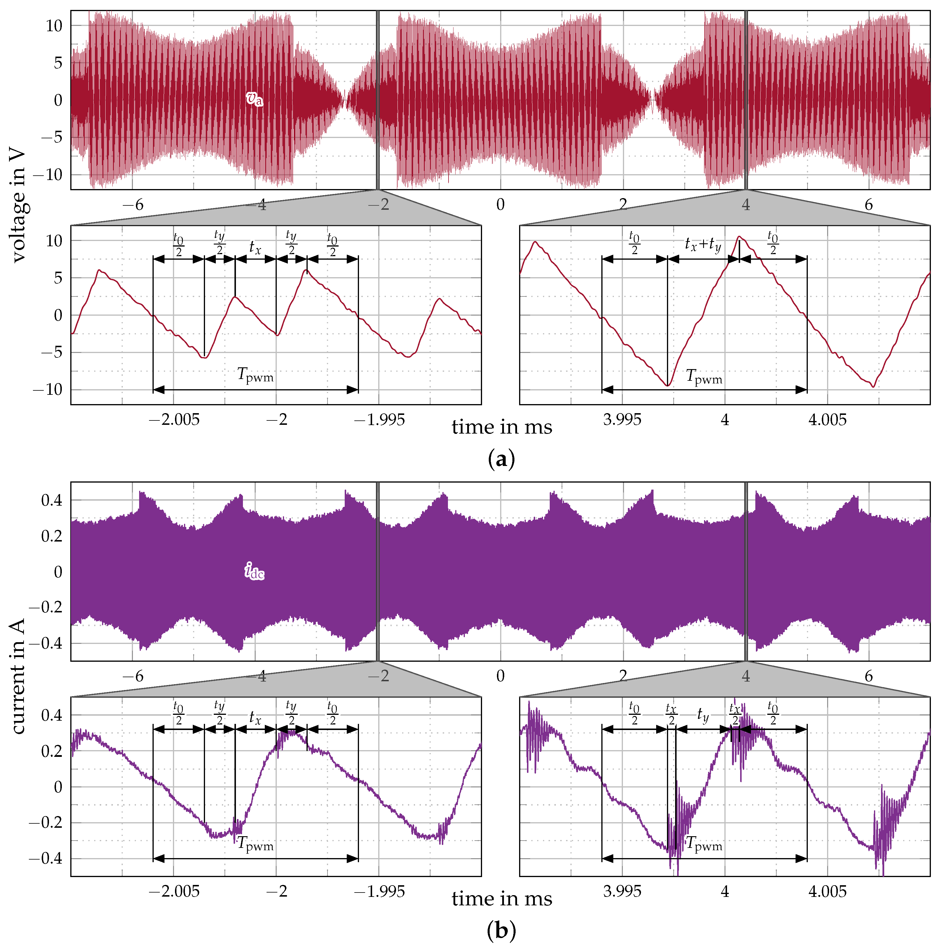
6. Experimental Verification
Experimental Results
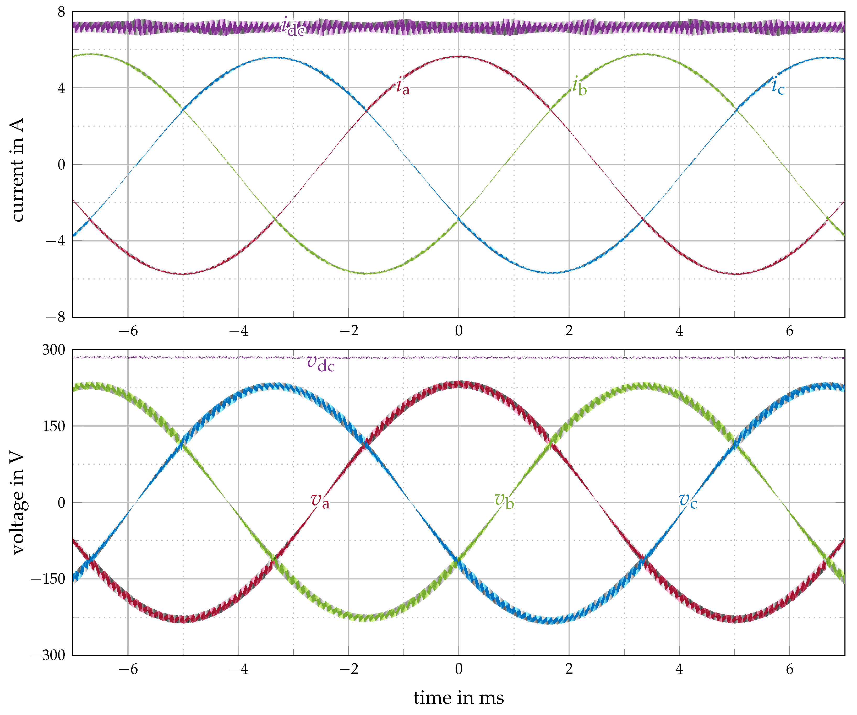
- The inverter was loaded with three resistors of , which behaves like the linear load as assumed during the design process, ensuring the rated output voltage of at and .
- The average DC-link current was maintained constant at 7 A with an appropriate DC power supply in constant current mode at the input.
- The PWM frequency was set to 100 kHz, the AC output frequency to 100 Hz (period 10 ms), and the modulation index was decreased in steps from to to reduce the output power from the nominal operating point.
- The DC-link current , the input voltage , the three output currents , , and , as well as the line-to-line output voltages , , and were measured using an oscilloscope (Tektronix 5 Series) with appropriate current clamps and differential voltage probes, resulting in a total measurement bandwidth of 50 MHz. The phase voltage quantities , , and were subsequently calculated from the measured line-to-line voltages via , , and to be able to compare the measurement results with the analytical derivations for the phase voltage ripple.
- The converter efficiency was measured using a HIOKI PW8001 power analyzer employing HIOKI U7005 current transducers.
7. Conclusions
Author Contributions
Funding
Data Availability Statement
Conflicts of Interest
Abbreviations
| MDPI | Multidisciplinary Digital Publishing Institute |
| CSI | Current source inverter |
| CSC | Current source converter |
| BD | Bidirectional |
| RVB | Reverse voltage blocking |
| FPGA | Field Programmable Gate Array |
| ADC | Analog to Digital Converter |
| PWM | Pulse Width Modulation |
| RVM | Reduced Voltage Modulation |
| SiC | Silicon Carbide |
| GaN | Gallium Nitride |
References
- Iannaccone, G.; Sbrana, C.; Morelli, I.; Strangio, S. Power Electronics Based on Wide-Bandgap Semiconductors: Opportunities and Challenges. IEEE Access 2021, 9, 139446–139456. [Google Scholar] [CrossRef]
- Dai, H.; Jahns, T.M. Comparative Investigation of PWM Current-Source Inverters for Future Machine Drives Using High-Frequency Wide-Bandgap Power Switches. In Proceedings of the 2018 IEEE Applied Power Electronics Conference and Exposition (APEC), San Antonio, TX, USA, 4–8 March 2018; pp. 2601–2608. [Google Scholar] [CrossRef]
- Kolar, J.W.; Anderson, J.A.; Miric, S.; Haider, M.; Guacci, M.; Antivachis, M.; Zulauf, G.; Menzi, D.; Niklaus, P.S.; Minibock, J.; et al. Application of WBG Power Devices in Future 3-Φ Variable Speed Drive Inverter Systems “How to Handle a Double-Edged Sword”. In Proceedings of the 2020 IEEE International Electron Devices Meeting (IEDM), San Francisco, CA, USA, 12–18 December 2020; pp. 27.7.1–27.7.4. [Google Scholar] [CrossRef]
- Jahns, T.M.; Sarlioglu, B. The Incredible Shrinking Motor Drive: Accelerating the Transition to Integrated Motor Drives. IEEE Power Electron. Mag. 2020, 7, 18–27. [Google Scholar] [CrossRef]
- Madonna, V.; Migliazza, G.; Giangrande, P.; Lorenzani, E.; Buticchi, G.; Galea, M. The Rebirth of the Current Source Inverter: Advantages for Aerospace Motor Design. IEEE Ind. Electron. Mag. 2019, 13, 65–76. [Google Scholar] [CrossRef]
- Kolar, J.W.; Friedli, T.; Rodriguez, J.; Wheeler, P.W. Review of Three-Phase PWM AC–AC Converter Topologies. IEEE Trans. Ind. Electron. 2011, 58, 4988–5006. [Google Scholar] [CrossRef]
- Kolar, J.W.; Huber, J. Next-Generation SiC/GaN Three-Phase Variable-Speed Drive Inverter Concepts. In Proceedings of the PCIM Europe 2021, International Exhibition and Conference for Power Electronics, Intelligent Motion, Renewable Energy and Energy Management, Nürnberg, Germany, 3–7 May 2021; VDE: Frankfurt am Main, Germany, 2021; pp. 1–5. [Google Scholar]
- Chen, F.; Lee, S.; Jahns, T.M.; Sarlioglu, B. Comprehensive Comparative Analysis: VSI-based vs. CSI-based Motor Drive Systems with Sinusoidal Output Voltage. In Proceedings of the 2024 IEEE Applied Power Electronics Conference and Exposition (APEC), Long Beach, CA, USA, 25–29 February 2024; pp. 1021–1027. [Google Scholar] [CrossRef]
- Friedli, T.; Round, S.D.; Hassler, D.; Kolar, J.W. Design and Performance of a 200 kHz All-SiC JFET Current Source Converter. In Proceedings of the 2008 IEEE Industry Applications Society Annual Meeting, Edmonton, AB, Canada, 5–9 October 2008; pp. 1–8. [Google Scholar] [CrossRef]
- Friedli, T.; Round, S.; Hassler, D.; Kolar, J. Design and Performance of a 200-kHz All-SiC JFET Current DC-Link Back-to-Back Converter. IEEE Trans. Ind. Appl. 2009, 45, 1868–1878. [Google Scholar] [CrossRef]
- Lefevre, G. Design of a Low Inductive Switching Cell Dedicated to SiC Based Current Source Inverter (CSI). In Proceedings of the CIPS 2018, 10th International Conference on Integrated Power Electronics Systems, Stuttgart, Germany, 20–22 March 2018. [Google Scholar]
- Lefevre, G.; Anthony, B.; Stéphane, C. A Cost-Controlled, Highly Efficient SiC-based Current Source Inverter Dedicated to Photovoltaic Applications. In Proceedings of the 2018 20th European Conference on Power Electronics and Applications (EPE’18 ECCE Europe), Riga, Latvia, 17–21 September 2018. [Google Scholar]
- Zacher, B.H.; Bauer, A.; Franck, K.; Schumann, C. 48 V Current Source Inverter with Bidirectional GaN eHEMT Switches for Low Inductance Machine Drives. In Proceedings of the 2023 25th European Conference on Power Electronics and Applications (EPE’23 ECCE Europe), Aalborg, Denmark, 4–8 September 2023; pp. 1–9. [Google Scholar] [CrossRef]
- Torres, R.A.; Dai, H.; Lee, W.; Jahns, T.M.; Sarlioglu, B. Current-Source Inverters for Integrated Motor Drives Using Wide-Bandgap Power Switches. In Proceedings of the 2018 IEEE Transportation Electrification Conference and Expo (ITEC), Long Beach, CA, USA, 13–15 June 2018; pp. 1002–1008. [Google Scholar] [CrossRef]
- Lee, W.; Torres, R.A.; Dai, H.; Jahns, T.M.; Sarlioglu, B. Integration and Cooling Strategies for WBG-based Current-Source Inverters-Based Motor Drives. In Proceedings of the 2021 IEEE Energy Conversion Congress and Exposition (ECCE), Vancouver, BC, Canada, 10–14 October 2021; pp. 5225–5232. [Google Scholar] [CrossRef]
- Torres, R.A.; Dai, H.; Lee, W.; Sarlioglu, B.; Jahns, T. Current-Source Inverter Integrated Motor Drives Using Dual-Gate Four-Quadrant Wide-Bandgap Power Switches. IEEE Trans. Ind. Appl. 2021, 57, 5183–5198. [Google Scholar] [CrossRef]
- Zhang, D.; Cao, D.; Huber, J.; Kolar, J.W. Three-Phase Synergetically Controlled Current DC-Link AC/DC Buck–Boost Converter With Two Independently Regulated DC Outputs. IEEE Trans. Power Electron. 2023, 38, 4195–4202. [Google Scholar] [CrossRef]
- Zhang, D.; Huber, J.; Kolar, J.W. A Three-Phase Synergetically Controlled Buck–Boost Current DC-Link EV Charger. IEEE Trans. Power Electron. 2023, 38, 15184–15198. [Google Scholar] [CrossRef]
- Zhang, D.; Cao, D.; Huber, J.; Everts, J.; Kolar, J.W. Nonisolated Three-Phase Current DC-Link Buck–Boost EV Charger With Virtual Output Midpoint Grounding and Ground Current Control. IEEE Trans. Transp. Electrif. 2024, 10, 1398–1413. [Google Scholar] [CrossRef]
- Halkosaari, T.; Tuusa, H. Optimal Vector Modulation of a PWM Current Source Converter According to Minimal Switching Losses. In Proceedings of the 2000 IEEE 31st Annual Power Electronics Specialists Conference. Conference Proceedings (Cat. No.00CH37018), Galway, Ireland, 18–23 June 2000; Volume 1, pp. 127–132. [Google Scholar] [CrossRef]
- Bierhoff, M.; Fuchs, F. Semiconductor Losses in Voltage Source and Current Source IGBT Converters Based on Analytical Derivation. In Proceedings of the 2004 IEEE 35th Annual Power Electronics Specialists Conference (IEEE Cat. No.04CH37551), Aachen, Germany, 20–25 June 2004; pp. 2836–2842. [Google Scholar] [CrossRef]
- Torres, R.A.; Dai, H.; Jahns, T.M.; Sarlioglu, B. Operation and Analysis of Current-Source Inverters Using Dual-Gate Four-Quadrant Wide-Bandgap Power Switches. In Proceedings of the 2019 IEEE Energy Conversion Congress and Exposition (ECCE), Baltimore, MD, USA, 29 September–3 October 2019; pp. 2353–2360. [Google Scholar] [CrossRef]
- Chen, F.; Lee, S.; Jahns, T.M.; Sarlioglu, B. A High-Accuracy Power Loss Model of SiC MOSFETs in Current Source Inverter Considering Current Commutation and Parasitic Parameters. In Proceedings of the 2022 IEEE Energy Conversion Congress and Exposition (ECCE), Detroit, MI, USA, 9–13 October 2022; pp. 1–8. [Google Scholar] [CrossRef]
- Chen, F.; Lee, S.; Torres, R.A.; Jahns, T.M.; Sarlioglu, B. Performance Evaluation and Loss Modeling of WBG Devices Based on a Novel Double-Pulse Test Method for Current Source Inverter. In Proceedings of the 2021 IEEE Transportation Electrification Conference & Expo (ITEC), Chicago, IL, USA, 21–25 June 2021; pp. 219–224. [Google Scholar] [CrossRef]
- Chen, F.; Lee, S.; Jahns, T.M.; Sarlioglu, B. Comprehensive Efficiency Analysis of Current Source Inverter Based on CSI-Type Double Pulse Test and Genetic Algorithm. In Proceedings of the 2021 IEEE Energy Conversion Congress and Exposition (ECCE), Vancouver, BC, Canada, 10–14 October 2021; pp. 4940–4947. [Google Scholar] [CrossRef]
- Ul-Hassan, M.; Luo, F. Influence of Layout Parasitics and Its Optimization in Two-Level Gallium-Nitride Based Current Source Inverter. In Proceedings of the 2022 IEEE Energy Conversion Congress and Exposition (ECCE), Detroit, MI, USA, 9–13 October 2022; pp. 1–6. [Google Scholar] [CrossRef]
- Rodrigues, L.G.A.; Lefevre, G.; Martin, J.; Ferrieux, J.P. Switching Cell Design Optimization of SiC-based Power Modules for Current Source Inverter Applications. In Proceedings of the 2017 19th European Conference on Power Electronics and Applications (EPE’17 ECCE Europe), Warsaw, Poland, 11–14 September 2017; pp. P.1–P.10. [Google Scholar] [CrossRef]
- Lee, S.; Chen, F.; Jahns, T.M.; Sarlioglu, B. Alternating Sequence and Zero Vector Modulation with Reduced Switching Losses and Common-Mode Voltage in Current Source Inverters. In Proceedings of the 2023 IEEE Applied Power Electronics Conference and Exposition (APEC), Orlando, FL, USA, 19–23 March 2023; pp. 2613–2619. [Google Scholar] [CrossRef]
- Li, P.; Zhang, J.; Wang, J.; Cai, X. A New Design Method for the DC Inductance in Current Source Converters. In Proceedings of the IECON 2016—42nd Annual Conference of the IEEE Industrial Electronics Society, Florence, Italy, 23–26 October 2016; pp. 3160–3165. [Google Scholar] [CrossRef]
- Torres, R.A.; Dai, H.; Jahns, T.M.; Sarlioglu, B. Design of High-Performance Toroidal DC-link Inductor for Current-Source Inverters. In Proceedings of the 2019 IEEE Applied Power Electronics Conference and Exposition (APEC), Anaheim, CA, USA, 17–21 March 2019; pp. 2694–2701. [Google Scholar] [CrossRef]
- Zhou, G.; Qian, H.; Zhang, Q.; Hu, X.; Wang, F.; Li, C. Weight Optimization Design Method of DC-link Inductor for Current Source Inverters. IET Conf. Proc. 2021, 2020, 1245–1248. [Google Scholar] [CrossRef]
- Riegler, B.; Mutze, A. Volume Comparison of Passive Components for Hard-Switching Current- and Voltage-Source-Inverters. In Proceedings of the 2021 IEEE Energy Conversion Congress and Exposition (ECCE), Vancouver, BC, Canada, 10–14 October 2021; pp. 1902–1909. [Google Scholar] [CrossRef]
- Lee, S.; Feng, W.; Chen, F.; Chen, K.; Jahns, T.M.; Sarlioglu, B. Modeling of RMS Current in CSI Filter Capacitor and Minimum Conduction Loss Operation of CSI-Fed PMSM Drives for Traction Applications. In Proceedings of the 2022 IEEE Transportation Electrification Conference & Expo (ITEC), Anaheim, CA, USA, 15–17 June 2022; pp. 720–726. [Google Scholar] [CrossRef]
- Torres, R.A.; Dai, H.; Lee, W.; Jahns, T.M.; Sarlioglu, B. Development of Current-Source-Inverter-based Integrated Motor Drives Using Wide-Bandgap Power Switches. In Proceedings of the 2019 IEEE 15th Brazilian Power Electronics Conference and 5th IEEE Southern Power Electronics Conference (COBEP/SPEC), Santos, Brazil, 1–4 December 2019; pp. 1–6. [Google Scholar] [CrossRef]
- Friedli, T. Comparative Evaluation of Three-Phase Si and SiC AC-AC Converter Systems. Ph.D. Thesis, ETH Zürich, Zürich, Switzerland, 2010. [Google Scholar]
- Zhang, D.; Leibl, M.; Mühlethaler, J.; Huber, J.; Kolar, J.W. Analytical Modeling and Comparison of EMI Pre-Filter Noise Emissions of Three-Phase Voltage and Current DC-Link Converters. IEEE Trans. Power Electron. 2024, 39, 14691–14707. [Google Scholar] [CrossRef]
- Nain, N.; Huber, J.; Kolar, J.W. Comparative Evaluation of Three-Phase AC-AC Voltage/Current-Source Converter Systems Employing Latest GaN Power Transistor Technology. In Proceedings of the 2022 International Power Electronics Conference (IPEC-Himeji 2022-ECCE Asia), Himeji, Japan, 15–19 May 2022; pp. 1726–1733. [Google Scholar] [CrossRef]
- Nain, N.; Zhang, D.; Huber, J.; Kolar, J.W.; Kin Leong, K.; Pandya, B. Synergetic Control of Three-Phase AC-AC Current-Source Converter Employing Monolithic Bidirectional 600 V GaN Transistors. In Proceedings of the 2021 IEEE 22nd Workshop on Control and Modelling of Power Electronics (COMPEL), Cartagena, Colombia, 2–5 November 2021; pp. 1–8. [Google Scholar] [CrossRef]
- Guacci, M.; Zhang, D.; Tatic, M.; Bortis, D.; Kolar, J.W.; Kinoshita, Y.; Ishida, H. Three-Phase Two-Third-PWM Buck-Boost Current Source Inverter System Employing Dual-Gate Monolithic Bidirectional GaN e-FETs. CPSS Trans. Power Electron. Appl. 2019, 4, 339–354. [Google Scholar] [CrossRef]
- Ming, L.; Ding, W.; Yin, C.; Xin, Z.; Loh, P.C. A Direct Carried-Based PWM Scheme with Reduced Switching Harmonics and Common-Mode Voltage for Current Source Converter. IEEE Trans. Power Electron. 2021, 36, 7783–7796. [Google Scholar] [CrossRef]
- Clarke, E. Circuit Analysis of AC Power Systems; Wiley: Hoboken, NJ, USA, 1943; Volume 1. [Google Scholar]
- Novotny, D.W.; Lipo, T.A. Vector Control and Dynamics of AC Drives, Repr ed.; Number 41 in Monographs in Electrical and Electronic Engineering; Clarendon Pr: Oxford, UK, 2005. [Google Scholar]
- Riegler, B.; Mütze, A. Switching Loss Measurement of Wide-Bandgap Reverse-Blocking Semiconductor Switches in Current-Source Converters. In Proceedings of the 2022 IEEE 7th Southern Power Electronics Conference (SPEC), Nadi, Fiji, 5–8 December 2022; pp. 1–6. [Google Scholar] [CrossRef]
- Ul-Hassan, M.; Emon, A.I.; Yuan, Z.; Peng, H.; Luo, F. Performance Comparison and Modelling of Instantaneous Current Sharing Amongst GaN HEMT Switch Configurations for Current Source Inverters. In Proceedings of the 2022 IEEE Applied Power Electronics Conference and Exposition (APEC), Houston, TX, USA, 20–24 March 2022; pp. 2014–2020. [Google Scholar] [CrossRef]
- Guacci, M.; Tatic, M.; Bortis, D.; Kolar, J.W.; Kinoshita, Y.; Ishida, H. Novel Three-Phase Two-Third-Modulated Buck-Boost Current Source Inverter System Employing Dual-Gate Monolithic Bidirectional GaN e-FETs. In Proceedings of the 2019 IEEE 10th International Symposium on Power Electronics for Distributed Generation Systems (PEDG), Xi’an, China, 3–6 June 2019; pp. 674–683. [Google Scholar] [CrossRef]
- Snelling, E.C. Soft Ferrites: Properties and Applications, 2nd ed.; Butterworths: London, UK, 1988. [Google Scholar]
- Steinmetz, C.P. On the Law of Hysteresis. Proc. IEEE 1984, 72, 197–221. [Google Scholar] [CrossRef]
- Li, J.; Abdallah, T.; Sullivan, C.R. Improved Calculation of Core Loss with Nonsinusoidal Waveforms. In Proceedings of the Conference Record of the 2001 IEEE Industry Applications Conference. 36th IAS Annual Meeting (Cat. No. 01CH37248), Chicago, IL, USA, 30 September–4 October 2001; Volume 4, pp. 2203–2210. [Google Scholar] [CrossRef]
- Venkatachalam, K.; Sullivan, C.; Abdallah, T.; Tacca, H. Accurate Prediction of Ferrite Core Loss with Nonsinusoidal Waveforms Using Only Steinmetz Parameters. In Proceedings of the 2002 IEEE Workshop on Computers in Power Electronics, 2002 Proceedings, Mayaguez, Puerto Rico, USA, 3–4 June 2002; pp. 36–41. [Google Scholar] [CrossRef]
- Reinert, J.; Brockmeyer, A.; De Doncker, R. Calculation of Losses in Ferro- and Ferrimagnetic Materials Based on the Modified Steinmetz Equation. IEEE Trans. Ind. Appl. 2001, 37, 1055–1061. [Google Scholar] [CrossRef]
- Muhlethaler, J.; Biela, J.; Kolar, J.W.; Ecklebe, A. Core Losses Under the DC Bias Condition Based on Steinmetz Parameters. IEEE Trans. Power Electron. 2012, 27, 953–963. [Google Scholar] [CrossRef]
- Bartoli, M.; Noferi, N.; Reatti, A.; Kazimierczuk, M. Modeling Litz-wire Winding Losses in High-Frequency Power Inductors. In Proceedings of the PESC Record, 27th Annual IEEE Power Electronics Specialists Conference, Baveno, Italy, 23–27 June 1996; Volume 2, pp. 1690–1696. [Google Scholar] [CrossRef]
- Reatti, A.; Kazimierczuk, M. Comparison of Various Methods for Calculating the AC Resistance of Inductors. IEEE Trans. Magn. 2002, 38, 1512–1518. [Google Scholar] [CrossRef]
- Riegler, B.; Lee, Y.; Castellazzi, A.; Hartmann, M. Efficiency Considerations of a 3 kW, All SiC Current-Source Converter. In Proceedings of the 2024 IEEE Energy Conversion Congress and Exposition (ECCE), Phoenix, AZ, USA, 20–24 October 2024. [Google Scholar]


| Parameter | Symbol | Value |
|---|---|---|
| Nominal output power | 3 kW | |
| Nominal output voltage | 200 V | |
| Nominal output current | 5 A | |
| DC-link current | 7 A | |
| Design switching frequency | 100 kHz |
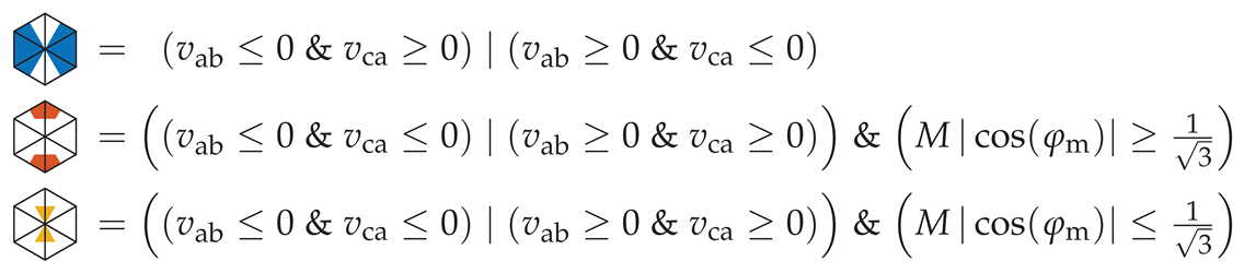
| Sector | Condition | Switching Cycle (● , ● ) |
|---|---|---|
 | ||
 | ||
 | ||
| Parameter | Symbol | Value |
|---|---|---|
| DC-link current | 7 A | |
| Nominal output voltage | 200 V | |
| Max. DC-link current ripple | 1.05 A (15% ) | |
| PWM switching frequency | 100 kHz | |
| DC-link inductance | μH | |
| Core | - | 59894A2 Edge |
| Number of stacked cores | cores | |
| Number of turns | N | turns |
| Wire length | m | |
| Wire diameter | 1 mm | |
| Max. core losses | mW @ | |
| Max. AC copper losses | mW @ | |
| Max. DC copper losses | W @ | |
| Max. temperature rise | 45.6 °C @ |
| Parameter | Symbol | Value |
|---|---|---|
| Nominal output power | 3 kW | |
| Nominal output voltage | 200 V | |
| Nominal output current | 5 A | |
| DC-link current | 7 A | |
| Maximum DC-link voltage | 500 V | |
| PWM switching frequency | 100 kHz | |
| DC-link inductance | μH (51 turns on 3 cores, ) | |
| Filter capacitance | (C0G in 2220 package) | |
| Power semiconductor | - | IMBG65R072M1H |
| CSI overlap time | 30 ns | |
| Converter dimensions | - | |
| Converter volume | 0.667 L | |
| Volumetric power density | 4.5 kW/L |
Disclaimer/Publisher’s Note: The statements, opinions and data contained in all publications are solely those of the individual author(s) and contributor(s) and not of MDPI and/or the editor(s). MDPI and/or the editor(s) disclaim responsibility for any injury to people or property resulting from any ideas, methods, instructions or products referred to in the content. |
© 2025 by the authors. Licensee MDPI, Basel, Switzerland. This article is an open access article distributed under the terms and conditions of the Creative Commons Attribution (CC BY) license (https://creativecommons.org/licenses/by/4.0/).
Share and Cite
Riegler, B.; Hartmann, M. Design and Implementation of 3 kW All-SiC Current Source Inverter. Electronics 2025, 14, 522. https://doi.org/10.3390/electronics14030522
Riegler B, Hartmann M. Design and Implementation of 3 kW All-SiC Current Source Inverter. Electronics. 2025; 14(3):522. https://doi.org/10.3390/electronics14030522
Chicago/Turabian StyleRiegler, Benedikt, and Michael Hartmann. 2025. "Design and Implementation of 3 kW All-SiC Current Source Inverter" Electronics 14, no. 3: 522. https://doi.org/10.3390/electronics14030522
APA StyleRiegler, B., & Hartmann, M. (2025). Design and Implementation of 3 kW All-SiC Current Source Inverter. Electronics, 14(3), 522. https://doi.org/10.3390/electronics14030522