Abstract
Traditional anti-counterfeiting techniques and methods are inadequate to meet the modern, sophisticated anti-counterfeiting requirement in banknotes. We applied our homemade near-field scanning microwave microscopy (NSMM) for penetrating imaging of concealed anti-counterfeiting features in banknotes. This NSMM imaged and characterized several vital concealed anti-counterfeiting features in the banknotes, including the dynamic color-shifting security threads, color-changing denomination numbers, magnetically embedded security threads, and white watermarks. At the same time, with the obstruction of red ink, near-field microwaves still penetrated the medium layer to characterize the detailed information of the security threads successfully. Additionally, the cavity perturbation method was used to obtain the effective permittivity of 3.65 and 3.62 for the windowing security thread and middle-embedded security thread. The thickness of the watermark was calculated to be about 3.3 μm with the calibrated fit method.
1. Introduction
Counterfeit techniques have posed a significant threat to global financial security. The academic community has proposed various banknote anti-counterfeiting methods to combat complex counterfeit techniques. These include controlling the distribution of pulp to form patterns with varying transparency [1], using nanowires to create a nanoscale coating as an anti-counterfeiting marker [2], using photo-switchable fluorescent polymer nanoparticles as anti-counterfeiting ink [3], developing flexible printing inks with unique security features [4], and so on. For the above anti-counterfeiting technologies, there are many detection techniques available on the market, such as using infrared spectroscopy, Raman spectroscopy, a video spectral comparator, atomic force microscopy (AFM), mass spectrometry, X-ray-based analytical techniques (XRF, XRPD), hyperspectral imaging (HSI), and sensors to detect specific physical, chemical, or optical properties in rust inhibitors. However, these detection technologies often have certain limitations, as shown in Table 1.

Table 1.
Summary of modern banknote anti-counterfeiting techniques.
The above techniques primarily target the chemical composition, printing features, optical characteristics, and physical structure of banknotes to verify whether they contain the correct security features. Modern counterfeiters use advanced scanning, printing, and copying equipment to accurately replicate the patterns, textures, and colors of banknotes, making it challenging for optical detection methods to distinguish them. They can also simulate certain chemical markers or physical features, such as the distribution of fluorescent substances or metal elements, to deceive detection devices based on chemical analysis and X-ray technology. Compared to the fifth series of Chinese Yuan (CNY) issued in 2005, the fifth series of CNY issued in 2019 presents several new anti-counterfeiting technologies, including color-changing denomination numbers, dynamic color-shifting security threads, and magnetically embedded security threads, instead of the previous holographic magnetic window security threads and intaglio tactile lines [12,13]. The magnetic security thread is a composite structure of magnetic particles and a polymer matrix. It comprises three layers; the middle layer is embedded with strips of magnetic material, while the top and bottom layers are made of cotton or linen fibers. The dynamic color-shifting security thread is fabricated from fiber materials (such as nylon, polyester, or other fibers) and photochromic ink containing photochromic agents (e.g., silver oxide, copper oxide, and iron oxide) and stabilizers [14]. These security threads are embedded inside the banknote, and windowing technology is utilized [15]. Due to the windowing process, the fully embedded security thread in the middle consists of three layers of paper, while the windowing security lines on both sides consist of two layers of paper. These security features are produced by directly removing or engraving materials with a laser to form hollowed-out numbers or patterns. These features provide an additional layer of protection against counterfeiting, ensuring the integrity of banknotes. When identifying multilayered and concealed security features, traditional detection instruments often encounter accuracy limitations. These limitations stem from the instruments’ inability to effectively penetrate and analyze the intricate layers and hidden elements integral to modern anti-counterfeiting measures. Additionally, many high-quality counterfeit magnetic materials and optically variable materials have emerged in the market. NSMM can penetrate top materials, such as the cotton or linen fibers of magnetic security threads and the topmost paper or ink layers of dynamic optical security threads. This allows for imaging electromagnetic properties of fine details within the intermediate layers. As a result, NSMM can precisely detect subtle electromagnetic differences, thereby accurately determining the authenticity of the CNY.
Among the numerous anti-counterfeiting technologies, microwave technology stands out due to its unique penetration capabilities and non-invasive nature. The development of NSMM has benefited from exploring electromagnetic properties in complex materials. Eric studied metallic domain walls in magnetic insulators, laying the foundation for applying NSMM in the study of microscopic electromagnetic properties [16]. Later, Yong developed a quartz tuning fork-based microwave impedance microscope, significantly improving the system’s resolution and sensitivity, advancing NSMM nanoscale applications [17]. Kim proposed a nanofocusing system that enables high-precision imaging without the need for lenses and enhances the capability for spectral and structural analysis at the nanoscale. Its breakthroughs in nanoscale imaging provide technical insights for improving the resolution of NSMM [18]. Ma further enhanced NSMM’s ability to probe sub-micrometer structures by achieving super-resolution imaging using a nanoscale white light source [19]. NSMM can obtain the material properties of the sample by analyzing the resonant frequency fr, quality factor Q, and phase ϕ [20,21]. Over the past few decades, NSMM has been used in many applications, such as imaging subsurface microstructure penetration [22], non-destructive testing of thin films [23,24], imaging of nanostructures [25], and semiconductor characterization [26,27], which present the possibility of NSMM application in penetrating imaging and characterizing electromagnetic properties.
Compared to common detection methods, NSMM has the following advantages [28,29,30,31]: (i) It can capture concealed details of anti-counterfeiting markers, especially microscopic structures that might be overlooked. (ii) NSMM offers non-destructive detection. (iii) NSMM can quantitatively detect the dielectric properties of materials, and it is highly sensitive to embedded elements in banknotes, such as metal wires or magnetic security features. (iv) NSMM can detect various materials, including magnetic, conductive, and non-conductive materials. (v) NSMM is not sensitive to environmental changes like humidity and temperature.
In this study, we conducted penetrating NSMM scans to investigate concealed anti-counterfeiting features in banknotes. We simulated conditions wherein banknotes are exposed to staining and conducted quantitative measurements of the electromagnetic properties associated with multi-layer concealed anti-counterfeiting features. Employing the cavity perturbation technique, we determined the effective permittivity of the windowing and middle-embedded security threads. Furthermore, the calibration fitting technique was utilized to ascertain the watermark’s thickness. NSMM enables detection without damaging the banknotes and provides detailed internal structural information, greatly enhancing the accuracy and reliability of banknote security verification.
2. Experimental Details
As shown in Figure 1, we developed an NSMM setup operating around 1.90 GHz. The size of the whole device is 60 × 43 × 50 cm3. It contains a one-quarter wavelength coaxial resonator, a vector network analyzer (VNA, Anritsu MS46122B-010, Shanghai, China), a three-axis motorized stage, a CCD optical camera, and a laptop computer. The VNA is used as both the microwave source and the detector, detecting parameters like resonant frequency fr, quality factor Q, and phase ϕ. In the experiment, we used a custom-designed quarter-wave coaxial resonator. The primary function of this resonator is to store and enhance microwave energy at its resonant frequency, creating a localized electromagnetic field. The inner conductor of the resonant cavity is equipped with a pin with a diameter of 50 μm, gathering electromagnetic fields at the probe’s tip. When the probe interacts with the sample surface, changes in the local electromagnetic properties of the sample perturb the resonator’s electromagnetic field, causing shifts in its resonant frequency and quality factor. The VNA connected to the resonator is used to continuously monitor these parameter changes in real-time, thereby mapping the electromagnetic properties of the sample surface. Additionally, the compact design of the quarter-wave resonator allows for high spatial resolution microwave detection, which is crucial for identifying minor electromagnetic variations on the sample surface. The near-field region between the probe and the sample allows for imaging and analysis of the surface and subsurface. An integrated LabVIEW program enables precise control of the setup and synchronous data logging. Since NSMM devices are highly susceptible to terrain artifacts, the device uses the terrain artifact removal algorithm instead of a distance sensor, such as a quartz fork, to avoid coupling between the sensor and the probe to reduce its sensitivity. Due to the nature of the material at the tamper-evident mark, the effect of the material on the resonant frequency of the point-scan results is small and almost negligible (Figure 2c). Hence, the artifact removal process takes advantage of the terrain sensitivity of the resonant frequency, establishing the capacitance-distance model to back-calculate the terrain image. The VNA uses a two-port setup, and S21 represents the ratio of the signal input at port 1 to its output at port 2. We assume that S21 can be separated as in [32]: . The linear effect of terrain height on S21 can be extracted by calculation: . The contribution of the sample attributes is expressed through the second term . Fixing the frequency fr and position (x, y), we can then measure the S21 variation with terrain height h. The parameter for the effect of topography was obtained by fitting the model . Once the terrain-influenced parameter has been determined, a correction can be made to S21. The setup is located within a double-layer standard machine case to minimize environmental noise and mechanical vibrations. The device mainly uses electromagnetic resonance perturbation theory. The probe is scanned point-by-point across the sample surface. Even small changes in the local electromagnetic properties of the sample can cause significant interference with the tip–sample interaction, resulting in changes in the electromagnetic waves reflected from the sample surface or from within the sample. These changes are reflected as changes in the resonant frequency fr and quality factor Q detected by the VNA. There are three types of scanning methods in our NSMM setup: point scanning, line scanning, and surface scanning. For point scanning, the first step is that the stage goes up and down in the z-direction but is fixed at a specific x–y position, and then the response changes that VNA would detect as the tip–sample distance varies; initially, when the probe tip gradually approaches the specimen, a relatively stable quality factor Q can be observed even when the distance changes, and this is called soft contact. For line scanning, the motor stage is fixed in the z-direction, and then the response information alone in the x or y direction (a line) is collected. To obtain surface scanning, the motor stage moves in a serpentine way forward with a fixed height. Our experiments were carried out on CNY 20 and CNY 50 of the fifth series in 2019, which are widely circulated in our daily lives. The banknotes used in the experiment were brand new to prevent other external factors from influencing the experiment. Red ink was also applied to brand-new banknotes. This research primarily investigates concealed details of these new anti-counterfeiting features in banknotes with the NSMM system.
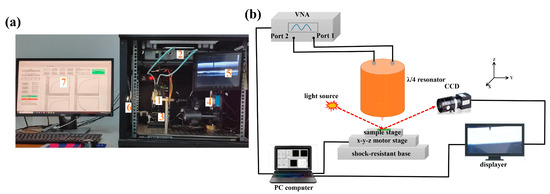
Figure 1.
NSMM setup. (a) Photograph of the home-designed NSMM system. (b) Schematic of the NSMM setup. (1) A λ/4 resonator, (2) a vector network analyzer (VNA), (3) a scanning platform attached to a three-axis motorized stage, (4) a CCD optical camera, (5) a piezoelectric motor, (6) a light source, and (7) a laptop computer. The size of the whole device is 60 × 43 × 50 cm3.

Figure 2.
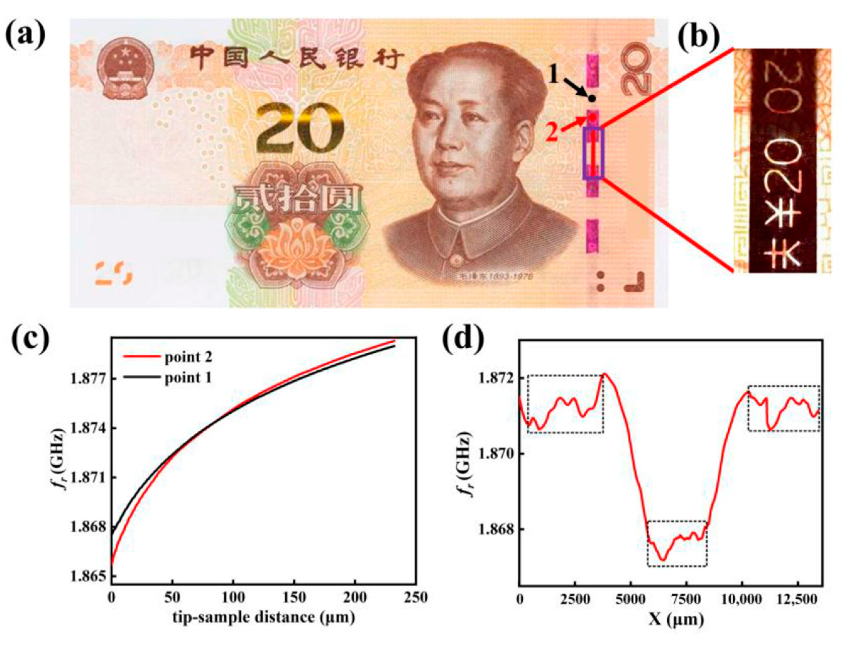
(a) CNY 20 issued in 2019. (b) Photograph of the purple rectangular region in (a) under transmitted light. (c) The fr with tip–sample distance scanned at points 1 and 2 in (a). (d) The fr was scanned in the red line of (a) at a tip–sample distance of 30 µm. The black dashed box fluctuations represent the detailed safety thread features.
3. Theoretical Analysis
The brand new CNY 20 banknote is studied with NSMM. We particularly focus on the dynamic color-shifting security thread on the right side of the banknote shown in Figure 2a. This security thread is embedded inside the banknote, and windowing technology is utilized. Therefore, it consists of windowing and fully embedded sections. The windowing section is composed of an upper layer featuring a security thread engraved with the number “20” and a lower layer of paper, while the fully embedded section consists of two layers of paper with the security thread in between. This security feature is crucial for counterfeit detection, and our goal is to demonstrate how NSMM can successfully visualize and measure its electromagnetic characteristics. By performing point scans at points 1 and 2 in Figure 2a, Figure 2c was obtained. Figure 2c shows the relationship between resonant frequency fr and the tip–sample distance. As the tip–sample distance increased, the fr for the two points showed a nonlinear increase. The resonant frequency fr can be determined by , where the effective capacitance (C) depends on the probe tip’s geometry, the sample’s characteristics, and the tip–sample distance. As the distance between the tip and the sample increases, the system’s equivalent circuit’s effective capacitance (C) decreases, leading to an increase in the resonant frequency fr. However, at the same tip–sample distance, the resonant frequency fr exhibited variations of two points due to differences in the material’s properties. Next, the windowing security thread was positioned under the tip, ensuring a distance of 30 μm between the tip and the thread. Then, five line scans were performed along the red path shown in Figure 2a. The scanning data were averaged, and noise reduction was applied using a filter, resulting in the data shown in Figure 2d. Due to the windowing process, the fully embedded security thread in the middle consists of three layers of paper, while the windowing security lines on both sides consist of two layers of paper. When the needle scans over the fully embedded security thread in the middle, the distance between the needle and the sample decreases, increasing the effective capacitance (C). Additionally, the electromagnetic properties of the material (such as conductivity and dielectric constant) further influence this effect, resulting in a decrease in the resonant frequency (fr), as shown by the valley in Figure 2d. Moreover, the tiny fluctuations in Figure 2d (black dashed box) correspond to the concealed features of the number 20, as shown in the dynamic color-shifting security thread of Figure 2b under transmitted light.
The other essential system parameters are the quality factor (Q) and phase (ϕ). The quality factor (Q) is physically defined as the ratio of the energy stored in the resonator to the energy dissipated per cycle [33], as in Equation (1).
where fr represents the resonant frequency, Etotal represents the average energy stored in the cavity, and Ploss represents the energy loss per second. For the NSMM system, as the total energy stored in the resonator remains constant, the quality factor Q is primarily influenced by energy losses, especially those caused by resistive heating in the sample material. As the distance between the probe and the sample surface increases, the energy loss decreases rapidly, which manifests as an increase in the quality factor Q in the experiments. The resonant frequency fr is mainly sensitive to the morphological features of the sample, while the quality factor Q more extensively reflects the electromagnetic properties of the sample. Another critical parameter is the phase ϕ. The phase provides essential information on signal delay, which can help analyze the electromagnetic characteristics of the sample, such as permittivity, magnetic permeability, etc., aiding in the identification of internal structures or defects within the sample [34].
We also employ NSMM to predict the dielectric properties of anti-counterfeit materials, thereby mitigating the counterfeiting of currency materials. Cavity perturbation theory is widely used to measure small changes in the electromagnetic properties of a sample. This theory is based on Maxwell’s equations and considers how the insertion of a small perturbation, such as a sample with unknown permittivity and permeability , affects the resonant frequency of a cavity. When a sample is placed inside the cavity, it causes a slight perturbation in the electric and magnetic fields, leading to shifts in the resonant frequency and quality factor, which the VNA can detect. These shifts are directly related to the dielectric and magnetic properties of the sample, allowing for precise characterization of material properties. Equation (2) is derived based on Maxwell’s equations, which describes the resonant frequency shift caused by changes in the electromagnetic properties of the sample within the cavity (). This formula can be found in classical electromagnetism textbooks (for example, see [Jackson, Classical Electrodynamics] [35] or [Pozar, Microwave Engineering] [36]). Equation (2) illustrates how changes in the sample’s permittivity affect the resonant frequency. Except for the perturbed electric field E, the resonant frequency f, and the sample’s permittivity , all other values are known cavity-related parameters. When the sample is placed within the near-field range of the probe tip, the radius of the tip and the practical field distribution range are much smaller than the wavelength. Thus, the electromagnetic waves can be regarded as quasi-static fields [37,38,39]. Hence, the mirror charge method can be used to analyze the distribution of static fields. Gao applied the image charge method to approximate the perturbed electric field E [40]. This is achieved by placing a virtual image charge at a suitable position in the system to replace the effect of induced or polarized charges caused by the source charge on the field distribution. Based on the uniqueness theorem, as long as the introduced virtual charge preserves the original system’s boundary conditions, the electric field’s solution is the same as the original system’s electric field solution. The mirror charge method under soft contact [41,42] is used to obtain an expression for the resonant frequency shift , as shown in Equations (3)–(5).
where f, E, and H are the resonant frequency, electric, and magnetic fields with the existence of the sample, respectively. Symbols with 0 subscript are referred to as the sample-free state. and are the permittivity and magnetic permeability of the sample. Prefix was used for changes caused by the sample perturbation. Both integrations are taken concerning the cavity volume v0. R0 is the radius of the tip, and R2 and R1 are the radii of the center and outer conductors, respectively. The expression for A applies only to the ideal l/4 coaxial resonator. A can be appropriately calibrated by measuring a standard sample such as sapphire with a known dielectric constant. (the measured materials are non-magnetic). Through this method, the frequency shift of the middle-embedded security thread and the windowing security thread on both sides is measured to be around 19.5 MHz and 19.8 MHz, respectively. Hence, effective permittivity is measured to be 3.62 and 3.65, respectively. This further verifies the precise difference in manufacturing materials in this anti-counterfeiting area. It is noteworthy that the errors caused by the approximation and the height of soft contact points are acceptable, with the standard deviations of the effective permittivity measured multiple times being 0.0017 and 0.0019. Additionally, the dielectric constant of a Teflon standard sample was measured at 2.07 (error = 1.4%). This demonstrates the stability and reliability of our instrument.
4. Results and Analysis
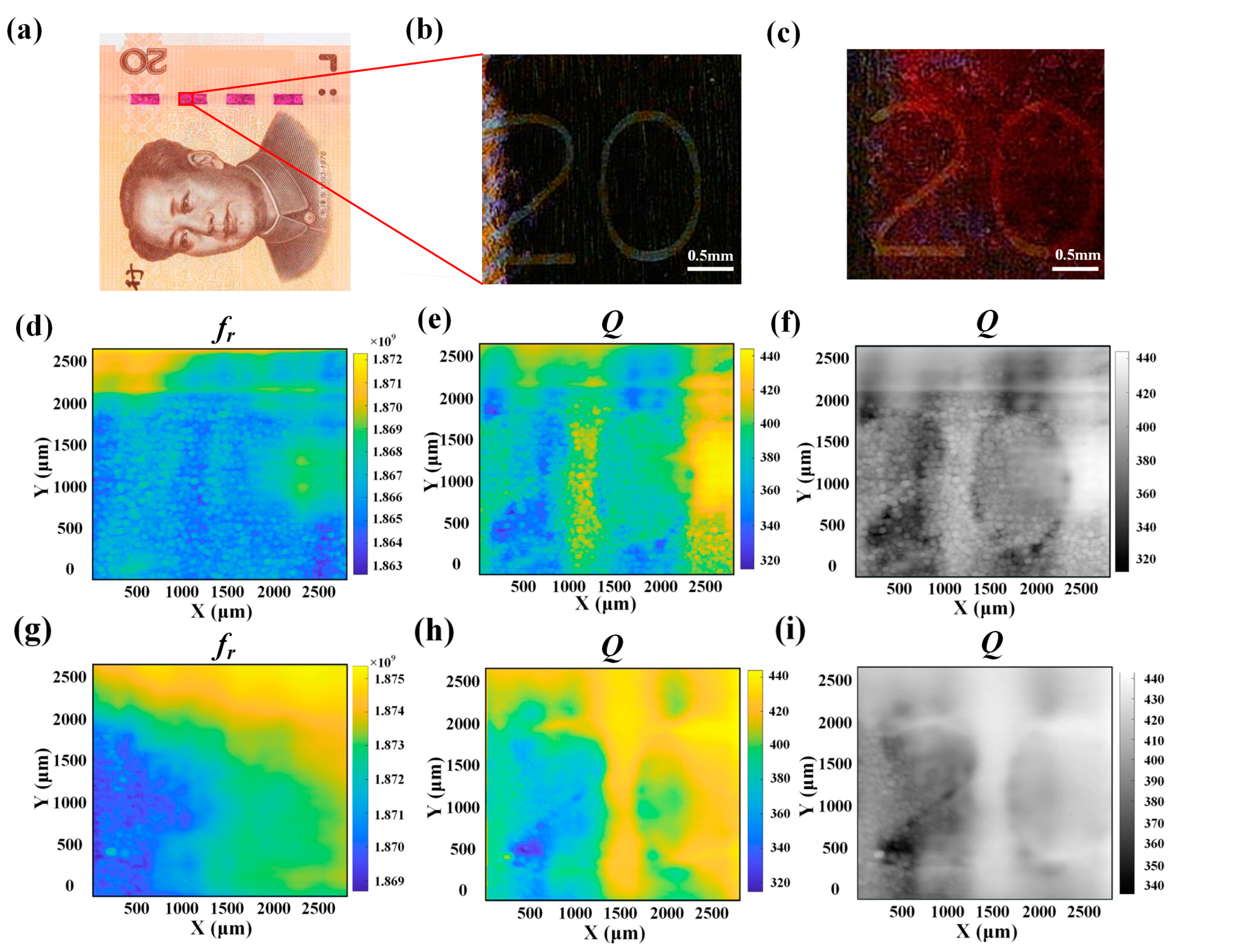
To better analyze the concealed anti-counterfeiting features. Figure 3b presents the image, observed under an optical microscope, of the red rectangular area in the CNY 20 of Figure 3a. This region contains the dynamic color-shifting security thread. The surface scan with NSMM aims to visualize the electromagnetic properties of this security feature, which is crucial for counterfeit detection. The size of the number 20 is 3 × 2 mm2. To enhance the imaging quality, we adjusted the distance between the probe tip and the sample to 5 μm and set the step size of the x–y motors to 250 μm. The penetration of near-field microwaves is applied when scanning the security thread of CNY 20. Contour maps of the resonant frequency fr (Figure 3d) and quality factor Q (Figure 3e) are generated. Considering that environmental factors may impact the NSMM scanning results, we performed the scans under different temperatures and humidity. The environment had little effect on the imaging results, and all concealed structures on the security thread could be identified. However, the fr image is not as good as that obtained by the quality factor Q image. In the near-field microwave penetration, the quality factor Q is more sensitive to the material’s electrical properties than resonant frequency fr. Figure 3e reveals that the dynamic color-shifting security thread material has a relatively strong capability to absorb or scatter microwaves, a kind of high energy loss material. Through the interaction between banknotes and near-field microwaves, subtle design patterns can be visualized. However, counterfeit methods targeting the manufacturing process and raw materials of the banknotes cannot reproduce the specific numeric patterns in these subtle features. In order to present stains that banknotes might encounter in circulation, a layer of red ink was applied as a marker on the security thread shown in Figure 3c. Subsequently, contour maps of the resonant frequency fr (Figure 3g) and quality factor Q (Figure 3h) are obtained. Grayscale maps generated in Figure 3f,i can present superior contrast and clarity. With the obstruction of red ink, near-field microwaves can still penetrate the medium layer to characterize the detailed information of the security thread on CNY 20. It demonstrates that the thin medium layer on the banknote’s surface has a minimal impact on the imaging results. The quality factor Q displays values significantly different from the surrounding security thread background, with a granular texture appearing in the image background. It indicates that near-field microwaves have penetrated the underlying paper material of the banknote. The ability of the microwaves to penetrate the red ink coating and reveal fine details of the thread structure underscores the effectiveness of NSMM for detecting concealed anti-counterfeiting features. The homemade NSMM system accurately identifies the concealed details on the banknote security thread. This finding highlights the significant advantages of NSMM in detail characterization, offering an effective tool for future banknote anti-counterfeiting and verification efforts.
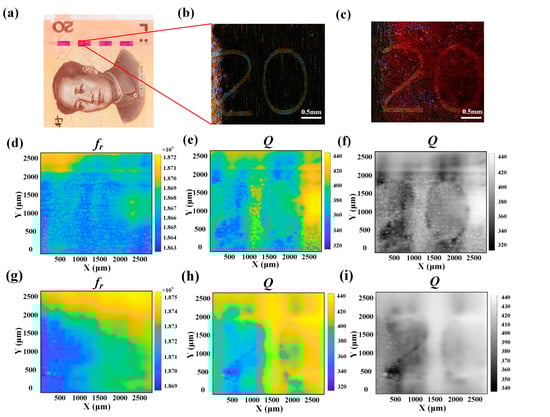
Figure 3.
(a) The security thread on CNY 20. (b) Image of the red rectangular region in (a). (c) The corresponding area of (b) is coated with red ink. The surface scan of (d) fr and (e) Q in area (b). The surface scan of (g) fr and (h) Q in area (c). Panels (f) and (i) are grayscale images of (e) and (h), respectively.
Because of the widespread circulation of the CNY 50 banknotes, the fifth series of CNY 50 issued in 2019 is selected as the object. Firstly, the white watermark of area I was tested, as shown in Figure 4a. Its optical image is shown in Figure 4b, with a region of 8×5 mm2. The distance between the tip and the sample is adjusted to 5 μm, and a surface scan of the watermark area in Figure 4b was performed, resulting in the contour maps of resonant frequency fr (Figure 4c) and quality factor Q (Figure 4d). They display patterns of the number 50 in the watermark. With the calibrated fit method, we subtract the frequency value of the number 5 from the frequency value of the background to obtain the frequency shift under soft contact. Then, we conduct a point scan of watermark 5 and the background, plotting two resonant frequency curves about the longitudinal distance. Lastly, we subtract the frequency values of the two curves to obtain frequency shift curves with longitudinal distance. The longitudinal distance corresponding to is the thickness of the watermark. So, the thickness of the watermark is estimated at 3.3 μm. It demonstrates that this homemade NSMM system can characterize the microstructural properties of materials.
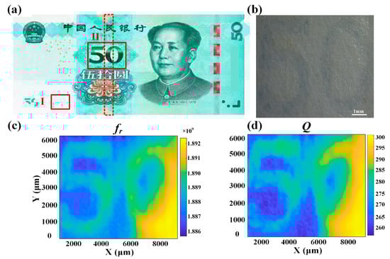
Figure 4.
(a) CNY 50 issued in 2019. Regions I and II represent the watermark and color-changing denomination numeral 50, respectively. The dashed outline denotes the invisible, magnetic, fully embedded security thread. (b) The optical image of region I in (a). The surface scan of (c) fr and (d) Q in area (b) at a tip–sample distance of 5 µm.
A surface scan of the purple rectangular area of color-changing denomination numbers in Figure 5a yielded the contour map of the resonant frequency fr shown in Figure 5c, which precisely corresponds to the optical photograph (Figure 5b) with the tip–sample distance of 10 μm. This map displays a thread with a significantly different resonant frequency fr from its surroundings, indicating the location of the magnetically embedded security thread. It cannot be seen with the naked eye, and its position in the banknote is random. In Figure 5c, a blurred number “0” can also be recognized on the magnetically embedded security thread. The blurred numeral “0” observed in Figure 5c corresponds to the concealed details of the magnetic security thread. Moreover, the magnetic security thread coincides with the color-changing denomination numbers in this experiment, forming a composite structure. To delve into the concealed detail features on the magnetic security thread, we performed a surface scan over the purple rectangular region highlighted in Figure 5b with a minimal tip–sample distance of 5 μm. The electromagnetic field concentrated near the tip interacted with the banknote, resulting in contour maps of the resonant frequency fr (Figure 5d), the quality factor Q (Figure 5e), and the phase ϕ (Figure 5f). Obvious numerical patterns of 50 can be observed in both the resonant frequency fr and the phase ϕ images. However, the numerical pattern is not discernible in the quality factor Q image. It indicates that the magnetic security thread exhibits differences in electromagnetic response characteristics and high signal-to-noise ratio due to its unique material composition and structural design. The lower quality factor Q can be attributed to the measurement apparatus’s differing inherent sensitivities and response characteristics. The distinct electromagnetic signatures, particularly in the fr and ϕ maps, provide strong evidence of the security thread’s multi-layered structure and complex material composition. The phase shift data, in particular, offers additional insight into the internal structure that is not visible through other methods. These results demonstrate that NSMM can penetrate the surface layers and accurately detect and visualize the fine details of anti-counterfeiting features, offering a robust method for banknote verification.
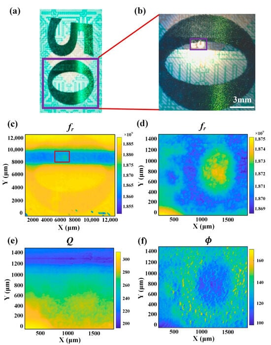
Figure 5.
(a) Photograph of region II in Figure 4a rotated clockwise by 90 degrees. (b) The purple rectangular region in (a). (c) The surface scan of fr in area (b) at a tip–sample distance of 10 µm. The surface scan of (d) fr, (e) Q, and (f) ϕ in the purple rectangular region in (b) at a tip–sample distance of 5 µm.
Table 2 summarizes the advantages and disadvantages of each detection method to clearly illustrate the main differences between NSMM and other current anti-counterfeiting detection methods.
Table 2.
Comparison of advantages and disadvantages of current anti-counterfeiting detection methods.
Unlike traditional methods, NSMM offers high spatial resolution and the ability to penetrate multiple embedded layers, allowing it to detect hidden security features with greater precision. Its sensitivity to conductive and non-conductive materials, combined with a lower overall cost, makes NSMM a promising alternative for widespread anti-counterfeiting applications, overcoming limitations found in existing technologies.
5. Conclusions
This study successfully developed an NSMM setup (60 × 43 × 50 cm3) for near-field microwave penetrating testing and imaging. NSMM images of concealed anti-counterfeiting features of CNY were obtained, including dynamic color-shifting security threads, color-changing denomination numbers, magnetically embedded security threads, and white watermarks. The detailed anti-counterfeiting features in staining conditions were also recognized successfully. The effective permittivity of 3.65 and 3.62 was measured for the windowing security thread and middle-embedded security thread, respectively, and the thickness of the watermark was calculated to be approximately 3.3 μm. NSMM’s high spatial resolution enables precise detection of hidden anti-counterfeiting features embedded within the layers of banknote materials, making it particularly effective for identifying sophisticated counterfeits that are difficult to detect using standard methods. Due to its relatively slow scanning speed, NSMM is unsuitable for high-traffic environments such as retail stores and restaurants, where rapid verification is essential. Instead, NSMM is best suited for specialized settings that require detailed analysis, such as laboratories or central banks, where accuracy takes precedence over speed. In these environments, NSMM can be a powerful supplementary tool for verifying suspicious currency or high-value documents that other detection methods might miss. Additionally, the watermarks, security threads, fluorescent ink in passports, holograms, optically variable patterns, and UV fluorescent patterns in identity cards (ID cards) have anti-counterfeiting features similar to those in banknotes. This demonstrates that NSMM can be applied to various security fields. In the future, path optimization algorithms and multi-point scanning techniques may be integrated with NSMM to enhance detection speed.
Author Contributions
Conceptualization, M.W., H.L. and P.H.; methodology, M.W. and Z.W.; formal analysis, M.W. and H.L.; investigation, M.W. and H.L.; resources, Z.W.; data curation, P.H.; writing—original draft preparation, M.W.; writing—review and editing, Z.W.; supervision, Z.W.; project administration, Z.W. All authors have read and agreed to the published version of the manuscript.
Funding
This work was supported by the Science and Technology Department of Sichuan Province (Grant No. 2020YJ0266), and the College Students’ Innovative Entrepreneurial Training for UESTC (Grant No. 202210614261X).
Data Availability Statement
The data that support the findings of this study are available from the corresponding authors upon reasonable request.
Conflicts of Interest
The authors have no conflicts to disclose.
References
- Bruna, G.M.; Farinella, G.C.; Battiato, S. Forgery detection and value identification of Euro banknotes. Sensors 2013, 13, 2515–2529. [Google Scholar] [CrossRef]
- Yang, R.L.; Zhu, Y.J.; Chen, F.F.; Dong, L.Y.; Xiong, Z.C. Luminescent; fire-resistant, and water-proof ultralong hydroxyapatite nanowire-based paper for multimode anticounterfeiting applications. ACS Appl. Mater. 2017, 9, 25455–25464. [Google Scholar] [CrossRef] [PubMed]
- Abdollahi, A.; Alidaei-Sharif, H.; Roghani-Mamaqani, H.; Herizchi, A. Photoswitchable fluorescent polymer nanoparticles as high-security anticounterfeiting materials for authentication and optical patterning. J. Mater. Chem. C 2020, 8, 5476–5493. [Google Scholar] [CrossRef]
- García-Lamont, F.; Cervantes, J.; López, A. Recognition of Mexican banknotes via their color and texture features. Expert Syst. Appl. 2012, 39, 9651–9660. [Google Scholar] [CrossRef]
- Vila, A.; Ferrer, N.; Mantecon, J.; Breton, D.; Garcia, J.F. Development of a Fast and Non-Destructive Procedure for Characterizing and Distinguishing Original and Fake Euro Note. Anal. Chim. Acta 2006, 559, 257–263. [Google Scholar] [CrossRef]
- Correia, R.M.; Domingos, E.; Tosato, F.; Aquino, L.F.M.; Fontes, A.M.W. Banknote Analysis by Portable near Infrared Spectroscopy. Forensic Chem. 2018, 8, 57–63. [Google Scholar] [CrossRef]
- de OB Brandão, J.M.; Almeida, N.S.; Dixini, P.V.; Baier, C.H.; Dias, H.P.; Romão, W. Documentoscopy by atomic force microscopy (AFM) coupled with Raman microspectroscopy: Applications in banknote and driver license analyses. Anal. Methods 2016, 8, 771–784. [Google Scholar] [CrossRef]
- Eberlin, L.S.; Haddad, R.; Neto, R.C.S.; Cosso, R.G.; Maia, D.R.J. Instantaneous Chemical Profiles of Banknotes by Ambient Mass Spectrometry. Analyst 2010, 135, 2533–2539. [Google Scholar] [CrossRef] [PubMed]
- Edelman, G.J.; Gaston, E.; Van Leeuwen, T.G.; Cullen, P.J.; Alders, M.C.G. Hyperspectral Imaging for Non-Contact Analysis of Forensic Traces. Forensic Sci. Int. 2012, 223, 28–39. [Google Scholar] [CrossRef]
- Marabello, D.; Benzi, P.; Lombardozzi, A.; Strano, M. X-Ray Powder Diffraction for Characterization of Raw Materials in Banknotes. J. Forensic Sci. 2017, 62, 962–970. [Google Scholar] [CrossRef] [PubMed]
- Lee, J.; Hong, H.; Kim, K.; Park, K. A Survey on Banknote Recognition Methods by Various Sensors. Sensors 2017, 17, 313. [Google Scholar] [CrossRef] [PubMed]
- China Banknote Printing and Minting Corporation. Anti-Counterfeiting Technologies, 1st ed.; The Fifth Series of Chinese Yuan (CNY); China Banknote Printing and Minting Corporation Official Publications: Beijing, China, 2019. [Google Scholar]
- People’s Bank of China. New Security Features; The Fifth Series of the Chinese Yuan; People’s Bank of China Official Press Release: Beijing, China, 2019.
- Wang, J.; Li, H.; Zhang, Q. Advancements in Security Thread Technology for Banknotes. J. Mater. Anti-Counterfeiting Sci. 2020, 15, 112–124. [Google Scholar]
- Liu, Y.; Chen, Z. Windowed Security Threads in Banknote Design: Techniques and Materials. Int. J. Currency Print. 2018, 8, 45–59. [Google Scholar]
- Ma, E.Y.; Cui, Y.T.; Ueda, K.; Tang, S.; Chen, K.; Tamura, N.; Wu, P.M.; Fujioka, J.; Tokura, Y.; Shen, Z.X. Mobile metallic domain walls in an all-in-all-out magnetic insulator. Science 2015, 350, 538–541. [Google Scholar] [CrossRef]
- Cui, Y.-T.; Ma, E.-Y.; Shen, Z.-X. Quartz tuning fork based microwave impedance microscopy. Rev. Sci. Instrum. 2016, 87, 063711. [Google Scholar] [CrossRef]
- Kim, S.; Yu, N.; Ma, X.; Zhu, Y.; Liu, Q.; Liu, M.; Yan, R. High external-efficiency nanofocusing for lens-free near-field optical nanoscopy. Nat. Photonics 2019, 13, 636–643. [Google Scholar] [CrossRef]
- Ma, X.; Liu, Q.; Yu, N.; Xu, D.; Kim, S.; Liu, Z.; Liu, M. 6 nm super-resolution optical transmission and scattering spectroscopic imaging of carbon nanotubes using a nanometer-scale white light source. Nat. Commun. 2021, 12, 6868. [Google Scholar] [CrossRef]
- Chu, Z.; Zheng, L.; Lai, K. Microwave microscopy and its applications. Annu. Rev. Mater. Res. 2020, 50, 105–130. [Google Scholar] [CrossRef]
- Gao, C.; Wei, T.; Duewer, F.; Lu, Y.; Xiang, X.D. High spatial resolution quantitative microwave impedance microscopy by a scanning tip microwave near-field microscope. Appl. Phys. Lett. 1997, 71, 1872–1874. [Google Scholar] [CrossRef]
- Sun, W.; Yang, Y.; Wu, Z.; Feng, T.; Zhuang, Q.; Peng, L.M.; Xu, S.; Ong, C.K. Penetrative imaging of sub-surface microstructures with a near-field microwave microscope. J. Appl. Phys. 2014, 116, 4. [Google Scholar] [CrossRef]
- Wu, Z.; Souza, A.D.; Peng, B.; Sun, W.Q.; Xu, S.Y.; Ong, C.K. Measurement of high frequency conductivity of oxide-doped anti-ferromagnetic thin film with a near-field scanning microwave microscope. AIP Adv. 2014, 4, 047114. [Google Scholar] [CrossRef]
- Wu, Z.; Du, Z.; Peng, K.; Gan, W.; Zhang, X.; Liu, G.; Zeng, B. Defect detection in graphene preparation based on near-field scanning microwave microscopy. IEEE Microw. Wirel. Components Lett. 2020, 30, 757–760. [Google Scholar] [CrossRef]
- Tabib-Azar, M.; Wang, Y. Design and fabrication of scanning near-field microwave probes compatible with atomic force microscopy to image embedded nanostructures. IEEE Trans. Microw. Theory Tech. 2004, 52, 971–979. [Google Scholar] [CrossRef]
- Reznik, N.; Korolyov, S.A.; Drozdov, M.N. Microwave microscopy of diamond semiconductor structures. J. Appl. Phys. 2017, 121, 164503. [Google Scholar] [CrossRef]
- Bagdad, B.A.; Lozano, C.; Gamiz, F. Near-field scanning microwave microscope platform based on a coaxial cavity resonator for the characterization of semiconductor structures. Solid State Electron. 2019, 159, 150–156. [Google Scholar] [CrossRef]
- Rosner, B.T.; Van Der Weide, D.W. High-frequency near-field microscopy. Rev. Sci. Instrum. 2002, 73, 2505–2525. [Google Scholar] [CrossRef]
- Anlage, S.M.; Talanov, V.V.; Schwartz, A.R. Principles of near-field microwave microscopy. In Scanning Probe Microscopy: Electrical and Electromechanical Phenomena at the Nanoscale; Springer: Berlin/Heidelberg, Germany, 2007; pp. 215–253. [Google Scholar]
- Kleismit, R.A.; Kazimierczuk, M.K.; Kozlowski, G. Sensitivity and resolution of evanescent microwave microscope. IEEE Trans. Microw. Theory Tech. 2006, 54, 639–647. [Google Scholar] [CrossRef]
- Xu, W.D.; Li, Z.C.; Liu, P.; Pei, Y.M. A Microwave Near-field 3D Super-resolution Imaging Method. Exp. Mech. 2021, 61, 859–866. [Google Scholar] [CrossRef]
- Fabi, G.; Joseph, C.H.; Pavoni, E.; Wang, X.P.; Al Hadi, R.; Hwang, J.C.M.; Morini, A.; Farina, M. Real-time removal of topographic artifacts in scanning microwave microscopy. IEEE Trans. Microw. Theory Tech. 2021, 69, 2662–2672. [Google Scholar] [CrossRef]
- Jordan, E.C.; Balmain, K.G. Electromagnetic Waves and Radiating Systems, 2nd ed.; Prentice Hall: Hoboken, NJ, USA, 1968. [Google Scholar]
- Bertotti, F.L.; Hara, M.S.; Abatti, P.J. A simple method to measure phase difference between sinusoidal signals. Rev. Sci. Instrum. 2010, 81, 115106. [Google Scholar] [CrossRef] [PubMed]
- Jackson, J.D. Classical Electrodynamics, 3rd ed.; Wiley: Hoboken, NJ, USA, 1998. [Google Scholar]
- Pozar, D.M. Microwave Engineering, 4th ed.; Wiley: Hoboken, NJ, USA, 2012. [Google Scholar]
- Gutierrez-Cano, J.D.; Plaza-Gonzalez, P.; Canos, A.J.; Garcia-Banos, B.; Catala-Civera, J.M.; Penaranda-Foix, F.L. A New Stand-Alone Microwave Instrument for Measuring the Complex Permittivity of Materials at Microwave Frequencies. IEEE Trans. Instrum. 2020, 69, 3595–3605. [Google Scholar] [CrossRef]
- Gregory, A.P.; Blackburn, J.F.; Lees, K.; Clarke, R.N.; Hodgetts, T.E.; Hanham, S.M.; Klein, N. Measurement of the permittivity and loss of high-loss materials using a Near-Field Scanning Microwave Microscope. Ultramicroscopy 2016, 161, 137–145. [Google Scholar] [CrossRef] [PubMed]
- Krupka, J. Frequency domain complex permittivity measurements at microwave frequencies. Meas. Sci. Technol. 2006, 17, 55–70. [Google Scholar] [CrossRef]
- Gao, C.; Xiang, X.D. Quantitative microwave near-field microscopy of dielectric properties. Rev. Sci. Instrum. 1998, 69, 3846–3851. [Google Scholar] [CrossRef]
- Steinhauer, D.E.; Vlahacos, C.P.; Wellstood, F.C.; Anlagea, S.M.; Canedy, C.; Ramesh, R.; Stanishevsky, A.; Melngailis, J. Quantitative imaging of dielectric permittivity and tunability with a near-field scanning microwave microscope. Rev. Sci. Instrum. 2000, 71, 2751–2758. [Google Scholar] [CrossRef]
- Gao, C.; Hu, B.; Takeuchi, I.; Chang, K.S.; Xiang, X.D.; Wang, G. Quantitative scanning evanescent microwave microscopy and its applications in characterization of functional materials libraries. Meas. Sci. Technol. 2004, 16, 248. [Google Scholar] [CrossRef]


Disclaimer/Publisher’s Note: The statements, opinions and data contained in all publications are solely those of the individual author(s) and contributor(s) and not of MDPI and/or the editor(s). MDPI and/or the editor(s) disclaim responsibility for any injury to people or property resulting from any ideas, methods, instructions or products referred to in the content. |
© 2024 by the authors. Licensee MDPI, Basel, Switzerland. This article is an open access article distributed under the terms and conditions of the Creative Commons Attribution (CC BY) license (https://creativecommons.org/licenses/by/4.0/).