Article

Alternative Performance Indices-Based Control Technique for a Unity Power Factor Three-Phase Rectifier

1
College of Engineering, Hebei Normal University, Shijiazhuang 050024, China
2
Hebei Provincial Key Laboratory of Information Fusion and Intelligent Control, Shijiazhuang 050024, China
3
Jiangsu Tailong Reducer Co., Ltd., Taizhou 225400, China
4
Hebei Science and Technology Engineering School, Baoding 071000, China
*
Author to whom correspondence should be addressed.
These authors contribute equally to this work.
Electronics 2024, 13(3), 604; https://doi.org/10.3390/electronics13030604
Submission received: 20 December 2023 / Revised: 23 January 2024 / Accepted: 30 January 2024 / Published: 1 February 2024
(This article belongs to the Section Power Electronics)

Abstract

:
The implementation of a unity power factor (UPF) three-phase rectifier has the potential to enhance the power factor (PF). However, the PF and total harmonic distortion (THD) experience degradation in low-output regions due to the utilization of a “critical input inductor” under rated load conditions. In this study, an analysis of the operation principle of a UPF three-phase rectifier is conducted and a reference compensation current technique based on alternative performance indices is proposed. The optimal control algorithm is utilized to calculate the single harmonic phase delay of each phase and determine the compensator gain, taking into account factors such as the single harmonic distortion limit, THD limit, PF, and active power consumption. The output of the current compensator serves as the desired current source, which in turn drives the bidirectional switches. The simulation and experimental results demonstrate that the proposed control technique can significantly mitigate power supply current distortion, and the input power factor has been effectively improved within a wider load range.

1. Introduction

The advancement and application of new energy generation technologies have led to the development of various technologies [1,2,3,4], including power factor correction in wind power generation [5,6,7]. Simultaneously, the increasing focus on environmental preservation has driven the widespread adoption of electric vehicles [8,9,10]. Nonetheless, electric vehicle charging processes can introduce harmonic pollution to the power grid [11,12,13]. Therefore, the enhancement in power factor during the charging of electric vehicles has emerged as a pressing issue to be addressed [14,15,16,17]. The improvement in power factor in the power grid can be accomplished through compensation or correction devices, as well as through the utilization of unit power factor (UPF) rectifiers [18,19]. The unit power factor rectifier combines rectification and power factor compensation functionalities. In addition to its applications in wind power generation and electric vehicle charging systems, it also finds utility in domains such as the variable frequency speed regulation of motors.
The power factor (PF) can be improved by using a UPF three-phase rectifier. The UPF rectifier consists of two series-connected capacitors, three input inductors and three bidirectional switches, as shown in Figure 1 [20,21,22,23,24]. The PWM rectifier requires twelve power switches (IGBT or MOSFET), whereas only three power switches are needed in the UPF rectifier. As a result, the UPF rectifier offers a significant advantage over PWM rectifiers due to its lower switching loss associated with the semiconductor power switches. Consequently, when compared to a PWM rectifier, the UPF rectifier can be more efficiently adopted as a front-end power factor pre-regulator for applications such as alternating current (AC) drivers or mode-switching power supplies.
The UPF three-phase rectifier achieves a PF of 0.99 and reduces the THD to 6.6% by employing bidirectional switches that conduct for a duration of 30 degrees of the line voltage when the phase voltage crosses 0 volts. This enables the rectifier to achieve a finely contoured sinusoidal input current waveform. The bidirectional switches conduct twice in a cycle, allowing the switching losses to be disregarded. It is important to note that both the PF and the THD are sensitive to load variation under this control strategy. Moreover, this technique is particularly effective when the rectifier is operating under specific load and input inductance conditions. Furthermore, the technique for reducing the input inductance of the converter involves increasing the switching frequency, which is the most efficient way to achieve this reduction. Additionally, as the DC link voltage fluctuates with changing load, enhanced performance is attained within a narrower power extent. This highlights the need for careful consideration of load conditions and input inductance when implementing this control strategy for the UPF rectifier.
The pursuit of advancing the performance of UPF rectifiers has led to the proposal of several control techniques [11,25,26,27,28]. These techniques aim to improve the characteristics and operation of UPF three-phase rectifiers across different power ranges. Some of the notable control methods include the following: A control method proposed in [26] considers the load, allowing the UPF three-phase rectifier to exhibit favorable characteristics across a broad power range. This approach takes into account the varying load conditions to optimize the performance of the rectifier. Another control method proposed in [25] involves comparing the error with the carrier signal to drive the bidirectional switches. While this method addresses the synchronization, it may still result in current errors due to the current ripple of the input inductor. An integrated control principle presented in [27] involves a constant switching frequency strategy without the use of voltage transformers. Nevertheless, the utilization of this method may result in severe distortion in the input current. In a method presented by Liu F. [28], a synchronous reference frame-based hysteresis current control is used as the inner loop, while voltage control is employed as the outer loop. However, the transformation of reference frames may extend the execution time of the controller for digital signal processing (DSP). Maswood A. I. presented a hysteresis current control method [29,30] in which the reference sinusoidal current is compared with the measured currents to facilitate the operation of bidirectional switches. While the method is relatively straightforward to implement, its utilization necessitates DC testing, leading to increased costs.
In this paper, a novel steady-state optimization technique has been introduced to enhance the control characteristics of UPF three-phase rectifiers. This technique aims to determine the reference compensation current effectively while considering alternative performance indices to satisfy all constraints. The primary focus is to demonstrate an optimal design for rectifier control, utilizing a current compensator to filter load currents and achieve sinusoidal and balanced source currents within the permissible range of distortion and imbalance. Additionally, this technique aims to adjust the power factor within a specific target range. The proposed approach considers two performance indices: maximizing PF and minimizing current distortion. The proposed method is particularly applicable when there are specific performance constraints that need to be met for the filter, especially in the presence of a non-linear load, such as rear-end inverters functioning as a load. Furthermore, the proposed control method is easily implemented using digital signal processing (DSP) for UPF three-phase rectifiers. The simulation and experimental results have demonstrated that the proposed control technique can effectively mitigate power supply current distortion. Moreover, within a broader load range, the input power factor has been significantly enhanced, showcasing the potential of the novel steady-state optimization technique to improve the performance of UPF three-phase rectifiers.

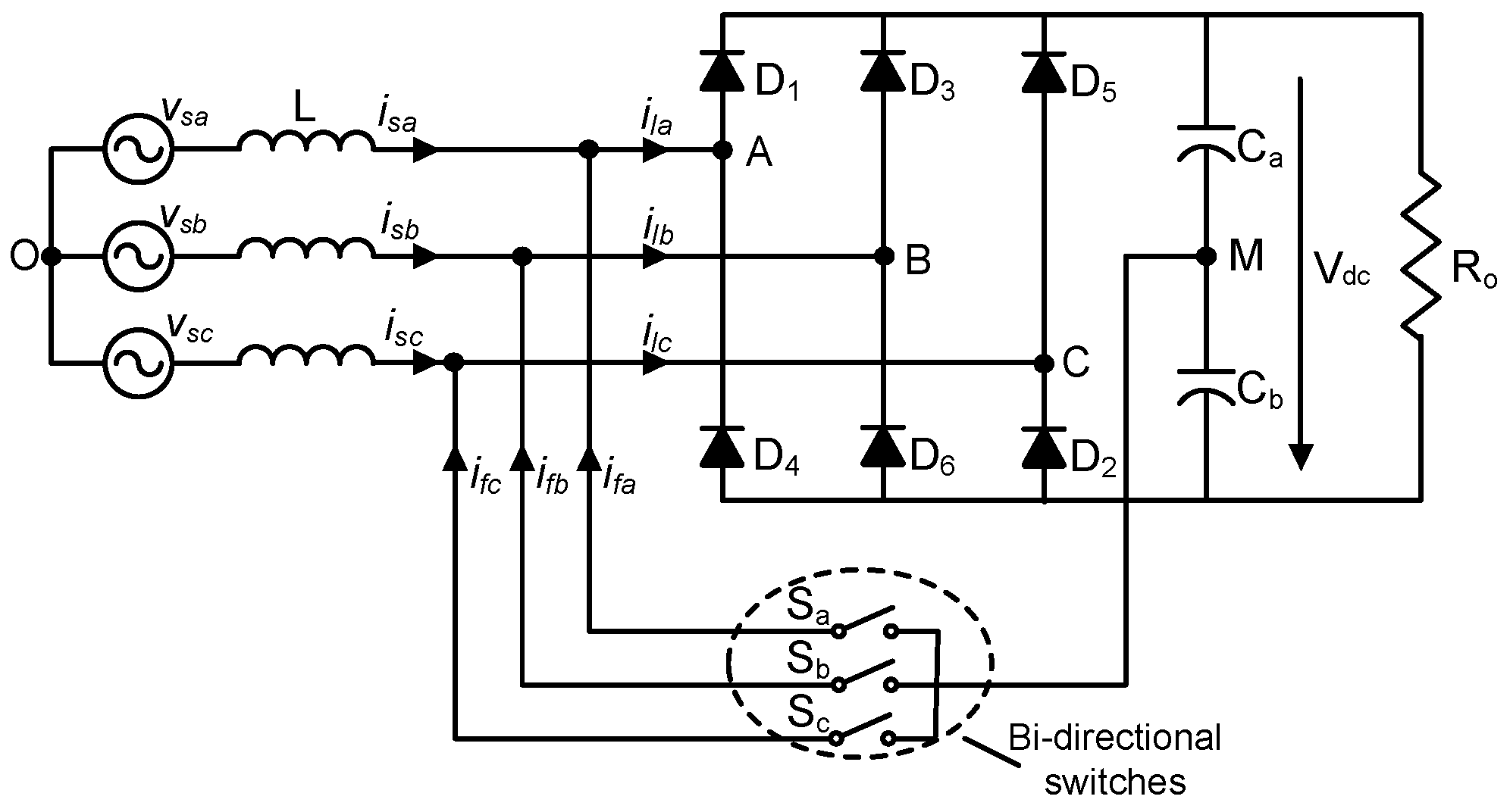
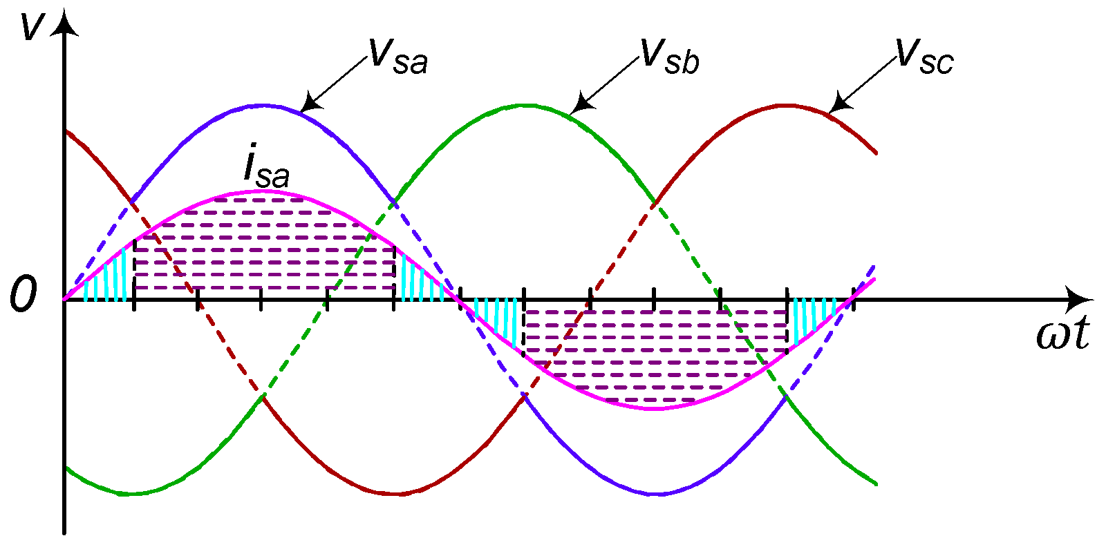
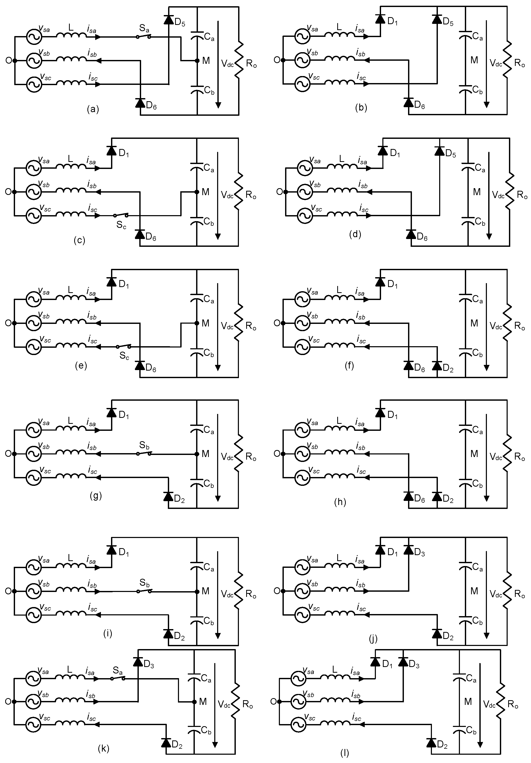
2. Operation Principle and Detailed Analysis of the Circuit

The rectifier circuit consists of a three-phase diode rectifier, two series-connected identical capacitors, and three bidirectional switches Sa, Sb, and Sc, as depicted in Figure 1. Each bidirectional switch consists of a MOSFET and four diodes, as shown in Figure 2.
To control the bidirectional switch, a hysteresis current control (HCC) method is utilized, ensuring that the input current follows a sine wave, stabilizing the DC side voltage, and maintaining rigorous balance in the voltage across the two capacitors. The voltage sources vsa, vsb, and vsc in Figure 1 represent the three-phase AC power supply. The corresponding voltage and a-phase current isa waveforms are illustrated in Figure 3.
Figure 4 illustrates six topological stages corresponding to the half-cycle (0° to 180°) of the phase voltage vsa. For ease of analysis, only the components with current flow in each stage are depicted.
  • Analysis of the operation of the scheme at interval I (0°–30°)
In Figure 4a,b, the polarity of vsa and vsc are positive, while vsb is negative. During the conduction of the bidirectional switch Sa, the power current isa flows through Sa, causing D5 and D6 to enter a conductive state. The non-illustrated diodes remain off in Figure 4a. Upon Sa disconnection, due to the inability of the inductor current to abruptly change, D1 continues to carry the current in the input inductor, while D5 and D6 remain conductive. Non-conducting diodes are not depicted in Figure 4b. The HCC controller determines the commutation time from Sa to D1. The conduction of D5 and D6 provides a rectification current, while the complementary conduction of Sa and D1 yields a compensation current.
Subsequent intervals, specifically (30°, 60°), (60°, 90°), (90°, 120°), (120°, 150°), and (150°, 180°), are analyzed in Figure 4 based on the same principle.
From the analysis, it is evident that the UPF three-phase rectifier circuit consists of two circuits: an ordinary rectifier and an active compensation-based network. The active compensation network comprises a bidirectional switch and a diode, which in a regular rectifier would be in the off state. The remaining diodes continue to form the ordinary rectifier. Therefore, the average active power consumed by the load is supplied by the ordinary rectifier, while the active compensation network neither consumes nor generates active power.

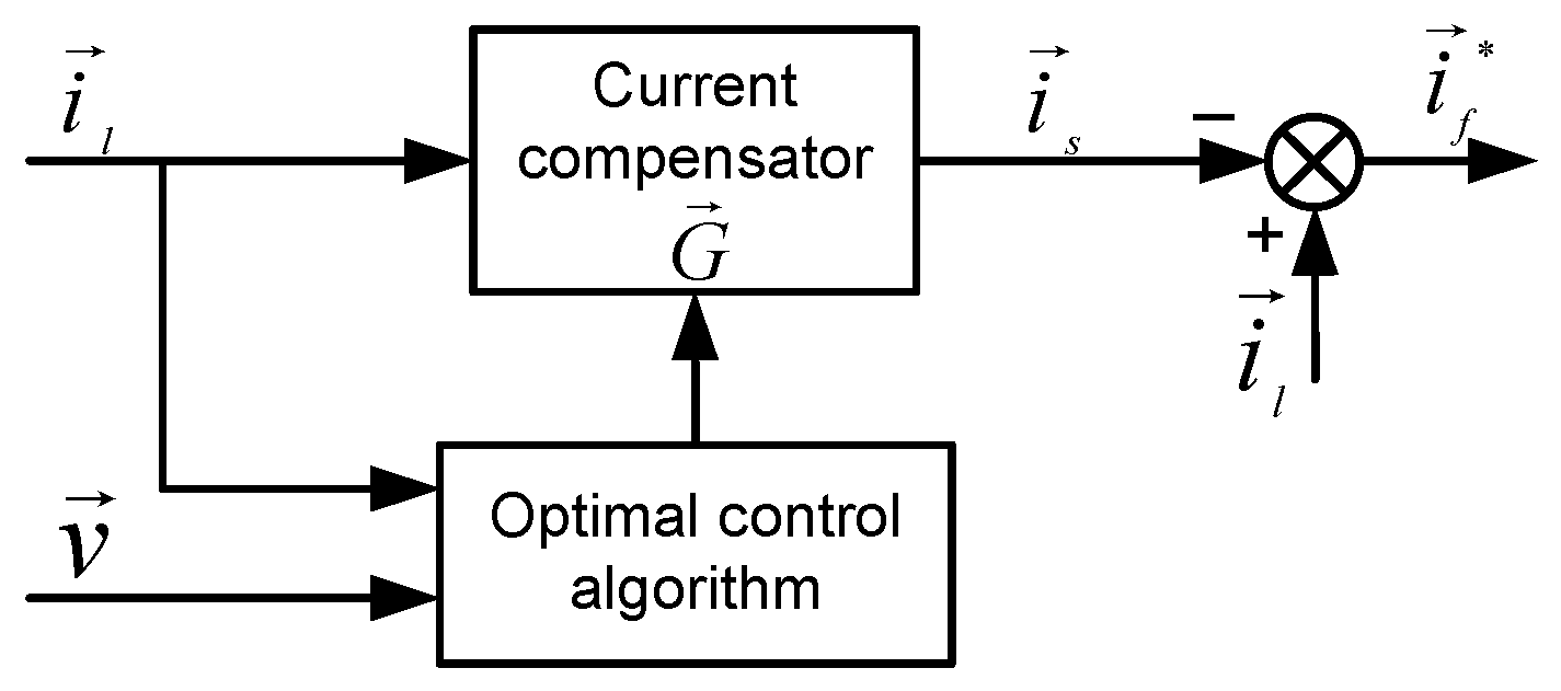
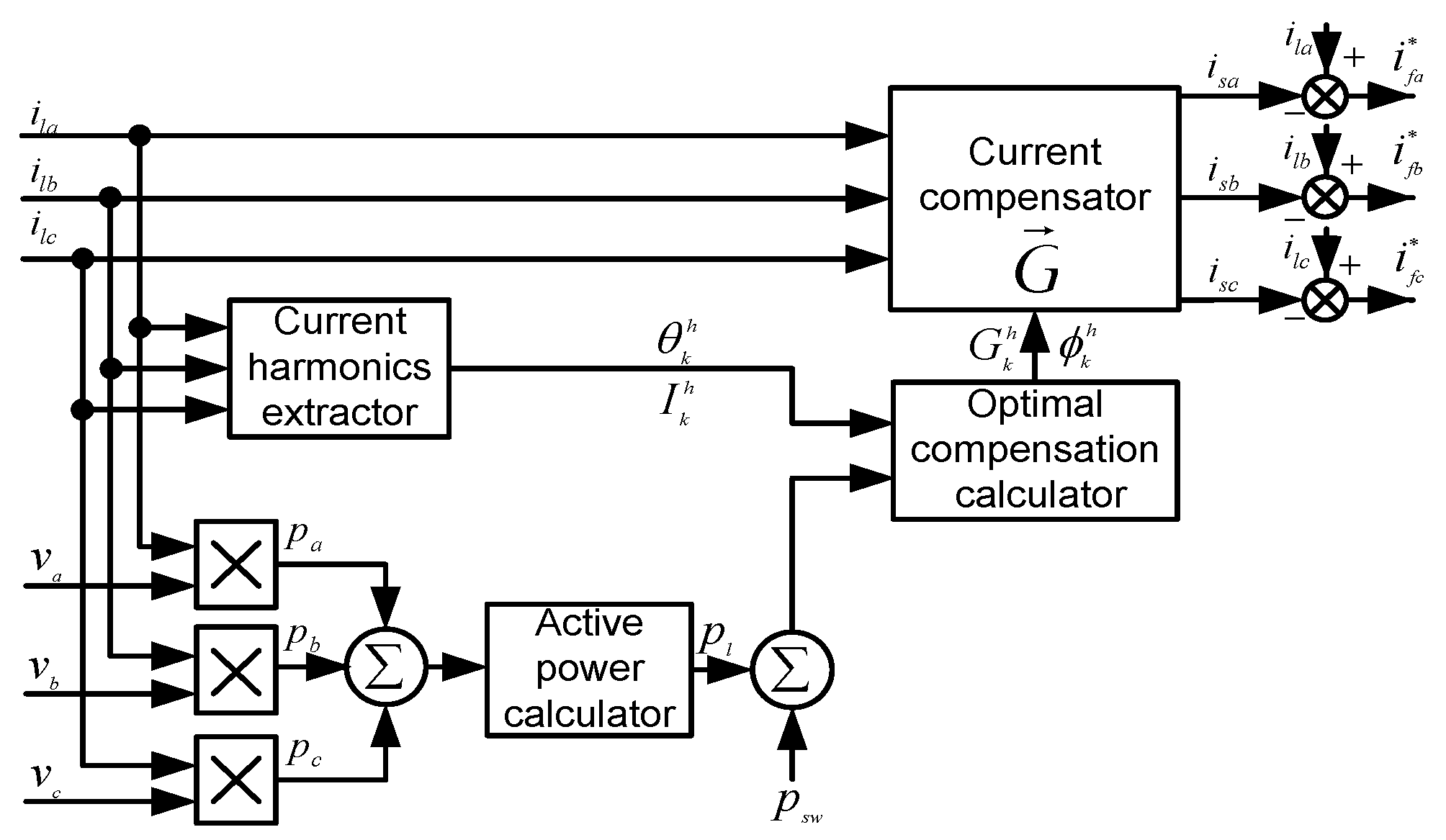
3. Proposed Optimal Control Technique for UPF Three-Phase Rectifier

3.1. Theoretical Calculation of Compensation Current

The compensation control technique proposed in this paper aims to achieve a balanced sinusoidal current after compensation, meeting the IEEE-519 standards [31]. To ensure compliance, the compensating current is derived by solving a non-linear problem using the optimal control algorithm depicted in Figure 5. Moreover, the voltage source itself may exhibit imbalance and distortion characteristics. Filtering the load current enables the attainment of the compensated current, while the optimal control algorithm is employed to determine the gain and phase delay of each harmonic in every phase of the compensator.
v is a three-phase voltage vector defined by Equation (1). i l represents the three-phase load current vectors and the compensated power supply current vectors as given in Equation (3) and Equation (4), respectively. In the frequency domain, the transform function of the compensator, represented as the ratio of i s to i l , is denoted by a vector G . Determining the transform function of the compensator is essential to ensure that the load current and compensated source currents conform to the relationship specified in Equation (4).
v = v s a v s b v s c ,
where [32]
v s a = h H 2 V a h sin h ω t + δ a h ; v s b = h H 2 V b h sin h ω t 2 π / 3 + δ b h ; v s c = h H 2 V c h sin h ω t + 2 π / 3 + δ c h ,
i l = i l a i l b i l c ,
i s = i s a i s b i s c = G i l .
Let the phase currents in i l be as follows [32]:
i l a = h H 2 I a h sin h ω t + θ a h ; i l b = h H 2 I b h sin h ω t 2 π / 3 + θ b h ; i l c = h H 2 I c h sin h ω t + 2 π / 3 + θ c h ,
Considering the order of the highest harmonic as N, then there is H = {1, 2, 3, …, N}. The source current of each harmonic in every phase after compensation i s must adhere to Equation (6), as depicted in Figure 5.
I ¯ s k h = G ¯ k h I ¯ l k h h H ,   k K ,
where G ¯ k h = G k h ϕ k h is the gain and phase delay of the hth harmonic in the k-phase of the compensator; I ¯ l k h = I k h θ k h is the load current phasor when K = {a, b, c}. Based on the above analysis, the power current vectors after compensation i s will be as follows:
i s a = h H 2 G a h I a h sin h ω t + θ a h + ϕ a h ; i s b = h H 2 G b h I b h sin h ω t 2 π / 3 + θ b h + ϕ b h ; i s c = h H 2 G c h I c h sin h ω t + 2 π / 3 + θ c h + ϕ c h .
Equations (3)–(7) illustrate that the optimal control method for the UPF rectifier entails a calculation process for both ideal and non-ideal power supply voltages to determine the gain and phase delay of each phase and harmonic of the compensated current. This process facilitates obtaining the reference compensation current for each phase of the rectifier by subtracting the compensated current from the load current, as follows:
i f k * = i l k i s k , k K .
The required Vrms and If,rms are determined by Equations (9) and (10).
V r m s = h H k K V k h 2 ,
I f , r m s = h H k K I f k h 2 ,
where V k h and I f k h are the valid values of power voltage and active compensation net of the hth harmonic in the k-phase, respectively.

3.2. Constraints

The gain and phase delay of the compensator for this rectifier will be thoroughly analyzed in this section.

3.2.1. Constraints on the Distortion of Single and Total Harmonics

Constraints on the distortion of a single harmonic of a compensated power supply current can be expressed as follows:
I H D I k h = I s k h I s k 1 α k h , h H ,   h 1 ,   k K .
Based on Equation (6), Equation (11) can be rearranged as follows:
I H D I k h = G k h I k h G k 1 I k 1 α k h .
Constraints on the distortion of the total harmonic of a compensated power supply current can be expressed by Equation (13).
T H D I k = h H I s k h 2 I s k 1 β k , h 1 ,   k K .
Similarly, Equation (12) can be rearranged to form Equation (14).
T H D I k = h H G k h I k h 2 G k 1 I k 1 β k .
In Equations (12) and (14), α k h and β k are standards for single and total harmonics in the k-phase in the standard IEEE-519 [31].

3.2.2. Constraints on PF of the Load

The compensated load PF is determined by Equation (15).
λ = P l V r m s I s , r m s ,
where Is,rms, Vrms, and Pl are determined by Equations (16), (9), and (17), respectively.
I s , r m s = h H k K I s k h 2 = h H k K G k h I k h 2 ,
P l = 1 T 0 T k K v k i l k d t .
According to standard IEEE-519 requirements, the compensated load PF is greater than or equal to λ ¯ , as follows:
λ = P l V r m s I s , r m s λ ¯ ,
Or the compensated power current is as follows:
I s , r m s I ¯ s ,
where I ¯ s = P l / λ ¯ V r m s .

3.2.3. Constraints on Consumption of Active Power

Constraints on the consumption of active power indicate that the active compensation network neither generates nor consumes any active components throughout the compensation process. This implies that all active power output from the power supply is consumed by the load. Consequently, the following relationship can be derived:
P f = 1 T 0 T k K v k i f k * d t = 0 ,
P s = 1 T 0 T k K v k i s k d t = P l .
Hence, substituting Equations (2) and (7) into Equation (21) gives the following equation:
k K h H V k h G k h I k h cos δ k h θ k h ϕ k h = P l .

3.2.4. Objective Function

The objective function of the active compensation network is to minimize the THD of the compensated three-phase power supply current while maximizing the PF of the load. This objective function is expressed as follows:
f o b j = k K T H D I k ,
where T H D I k is determined by Equation (14).
The compensated PF of the load is determined by Equation (15), with Vrms and Pl known before compensation. The maximum PF of the load aligns with the minimum power supply current after compensation. Therefore, the objective function is transformed into the following:
f o b j = I s , r m s ,
where Is,rms is determined by Equation (16).
In summary, the constrained optimization problems related to Equations (11)–(24) for calculating the gain G k h and phase delay ϕ k h of each harmonic in each phase after compensation, while considering various performance indices, are addressed by minimizing the fobj subject to the following:
I H D I k h α k h ,   h H ,   h 1 ,   k K ; T H D I k β k , h 1 ,   k K ; I s , r m s I ¯ s ; k K h H V k h G k h I k h cos δ k h θ k h ϕ k h = P l .

3.3. Method for Solving Constraints

The optimal control (i.e., Equation (25)) of the UPF three-phase rectifier involves constrained optimization, with all objective functions related to the constraints displaying highly non-linear behavior. The Optimization Toolbox in MATLAB 2021b is utilized for solving the constrained optimization due to its efficient algorithms [33]. Specifically, the toolbox’s Sequential Quadratic Programming method is employed to obtain the optimal solutions for the constrained problem. A significant advantage of this toolbox is its compatibility with MATLAB/Simulink, enabling an integrated simulation environment that is both computationally efficient and capable of delivering precise solutions.

4. Modeling the UPF Three-Phase Rectifier Using MATLAB

To validate the unique characteristics of the proposed control method for the UPF three-phase rectifier, a simulation model was established in MATLAB, as depicted in Figure 6. The simulation model primarily consists of the HCC, an optimal compensation current calculator, and the UPF three-phase rectifier linked with a PI controller for DC voltage, which compares the actual value of the DC voltage vdc with its corresponding reference value v*dc and outputs the active loss p s w . This also includes the losses of bidirectional switches and the capacitor at the DC side. The parameters of the PI controller are Kp = 1, and Ki = 0.001, respectively.
By employing the proposed control method, the calculation of the reference compensation current for the UPF three-phase rectifier in Figure 6 was achieved. The performance of the active compensation network aligns with the indicators calculated in Equations (23) and (24). To optimize the constraints of the UPF three-phase rectifier, it is necessary to determine the gain and phase delay for each harmonic of the optimal current compensator.
To calculate the optimal reference compensation current, the block diagram of the proposed control method is depicted in Figure 7. The current harmonic extractor algorithm is employed to derive the magnitudes and phase angles of all harmonics in a three-phase load current. The load active power is determined using an active power calculator, which is based on the average micro time of active power sampled over a fundamental period. Both the harmonic current and active power serve as input into the optimal compensator for calculation, enabling the derivation of the required gain and phase delay of the current compensator. The transform function of the compensator is multiplied by the load current to yield the required power current for each phase. The compensated current is then subtracted from the load current to yield the reference compensation current in each phase. Subsequently, upon passing through the harmonic compensation current (HCC) in Figure 6, the driving signal for the bidirectional switch is obtained.

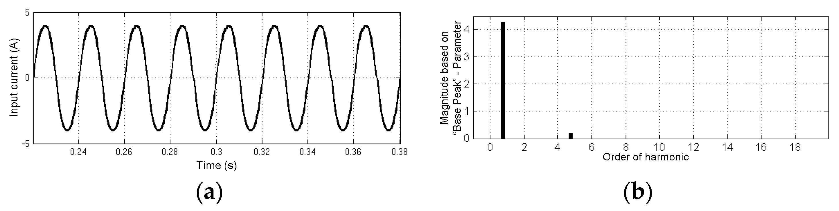
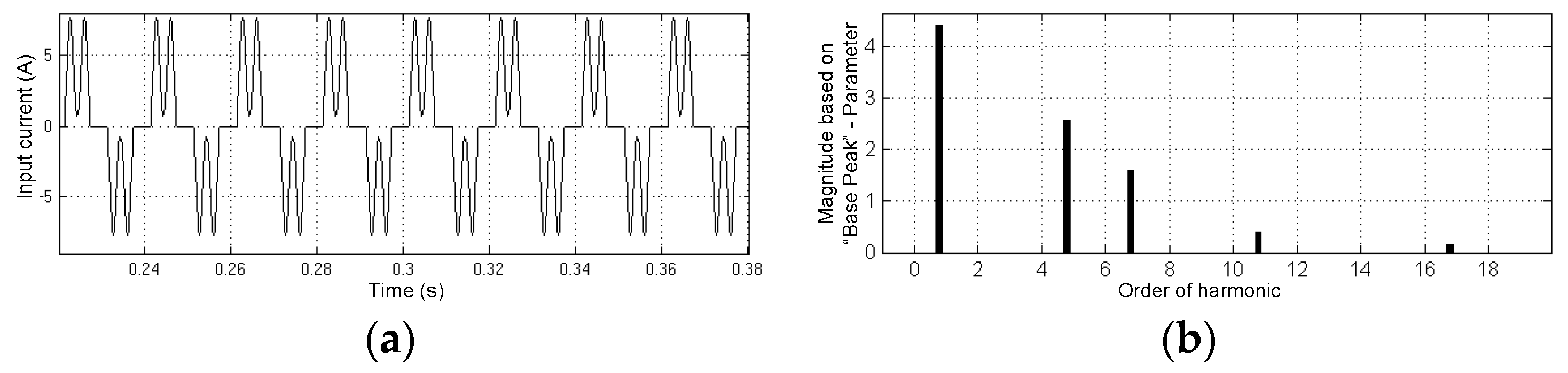
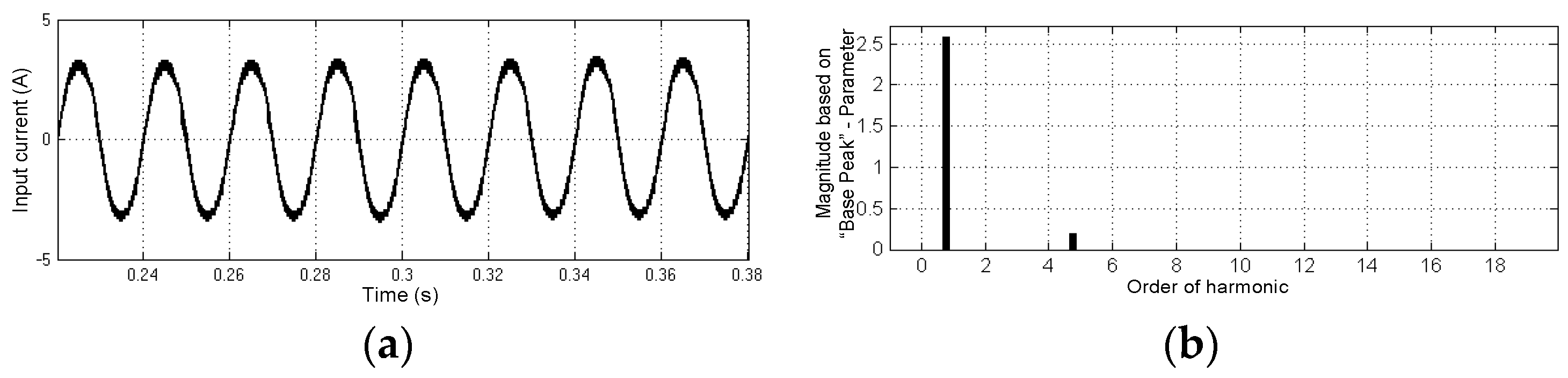
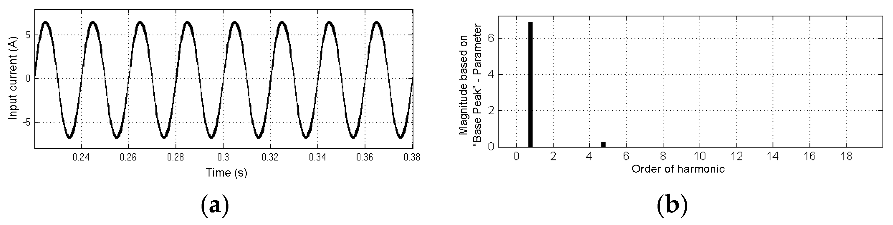
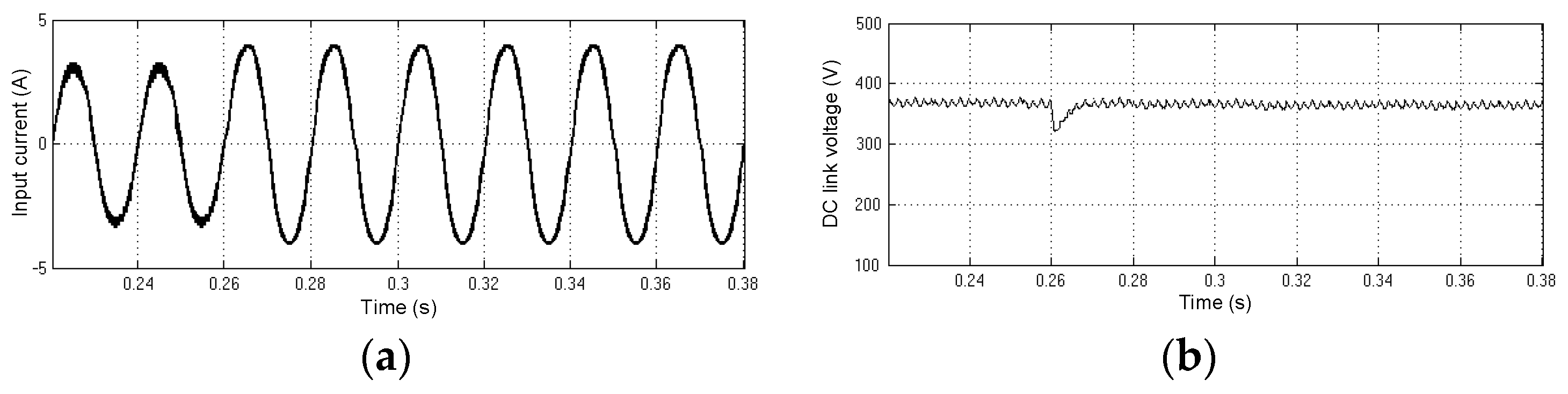
5. Simulation Results

To verify the distinctive characteristics of the proposed compensation control method for the UPF three-phase rectifier, a simulation model illustrated in Figure 6 was established. A sinusoidal PWM (SPWM) voltage source inverter was employed as the DC/AC inverter, which is a commonly used circuit in industry as a rectifier–inverter AC motor drive, as shown in Figure 8.
The distortion constraints for the compensation power supply current, as defined by Equations (12) and (14), are set to 5% and 6%, respectively. Additionally, the minimum load power factor constraint specified in Equation (18) is set to 0.95.
The prototype parameters are detailed in Table 1.
Figure 9 displays the waveform and harmonic spectrum of the input phase current of the UPF converter under the proposed control at rated power. Meanwhile, the corresponding waveform of the traditional converter is depicted in Figure 10.
A comparison of Figure 9 and Figure 10 reveals that the rectifier exhibited a high THD of 91.5% and a PF of just 0.72 before compensation. In contrast, after compensation, the THD dropped significantly to 3.8%, and the PF surged to 0.999. This indicates that the proposed reference compensation current method led to a considerable reduction in harmonics and a notable improvement in power factor.
Furthermore, an analysis was carried out to assess the converter’s performance under varying load conditions, both below and above its rated value. When operating at 50% of the rated output power, the input phase current waveform and its harmonic spectrum are illustrated in Figure 11. At this operating point, the converter demonstrates a high input PF of 0.996, alongside a THD of 4.0%.
At 150% of the rated output power, the converter’s input phase current waveform and its harmonic spectrum are depicted in Figure 12. The converter showcases a high PF of 0.999, along with a THD of 3.7%. These results demonstrate the favorable characteristics of the proposed control method across a range of varying load conditions and power levels.
Figure 13 illustrates the waveforms of the input phase current and DC link voltage in response to a sudden change in the converter’s output power from 50% to 100% of its rated value due to a load disturbance. During stable operation, the load changes at 0.26 s. The converter is observed to swiftly return to a steady DC link voltage in less than 0.01 s, demonstrating its robust response to sudden load variations. Therefore, the proposed control method exhibits commendable flexibility in accommodating load variations.

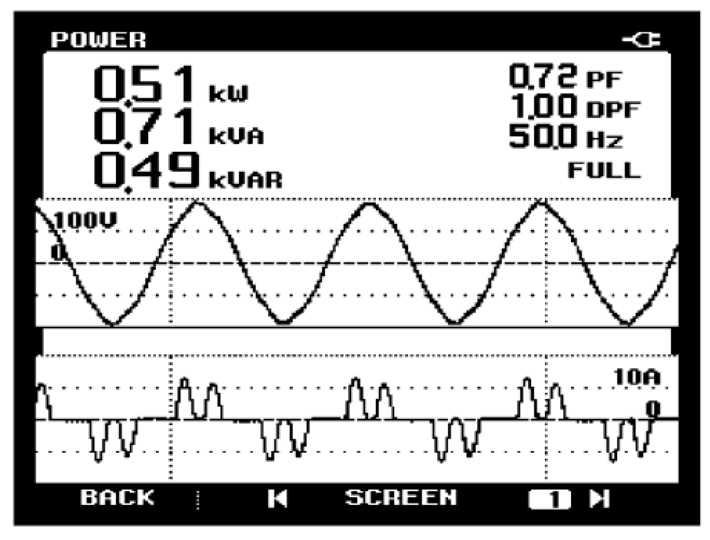
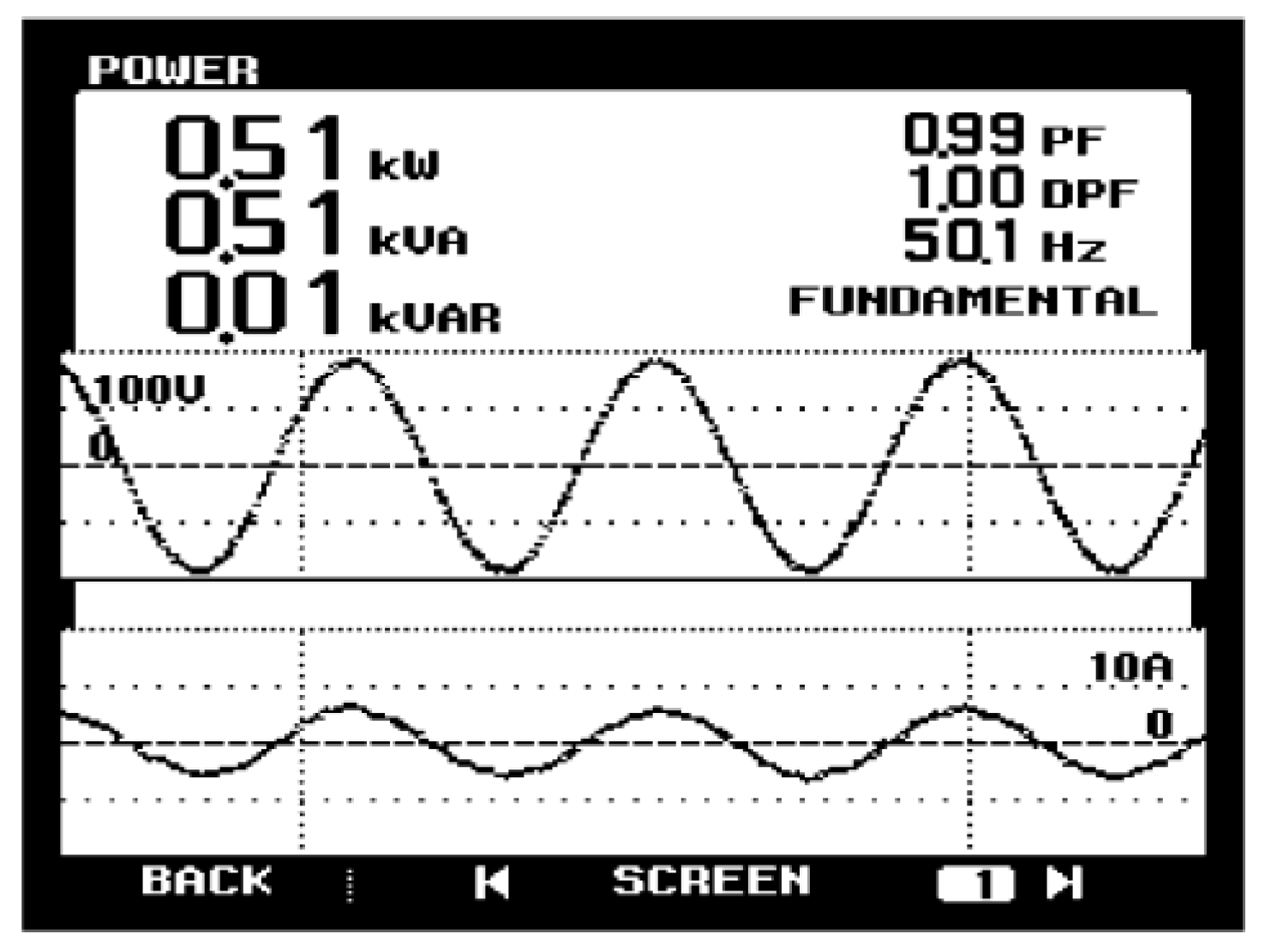
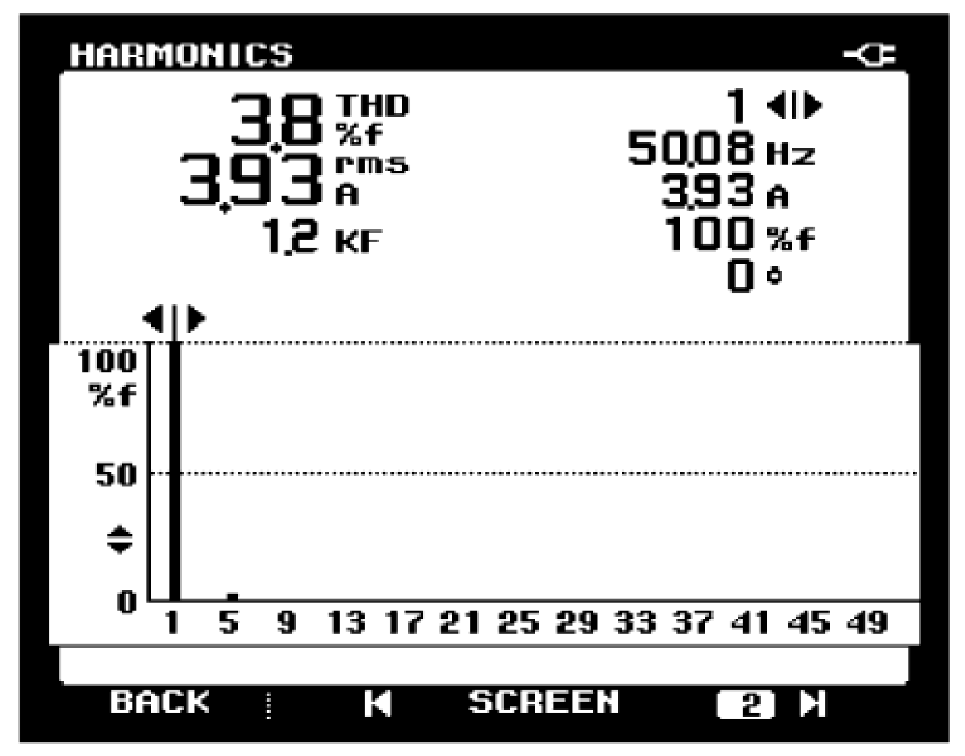
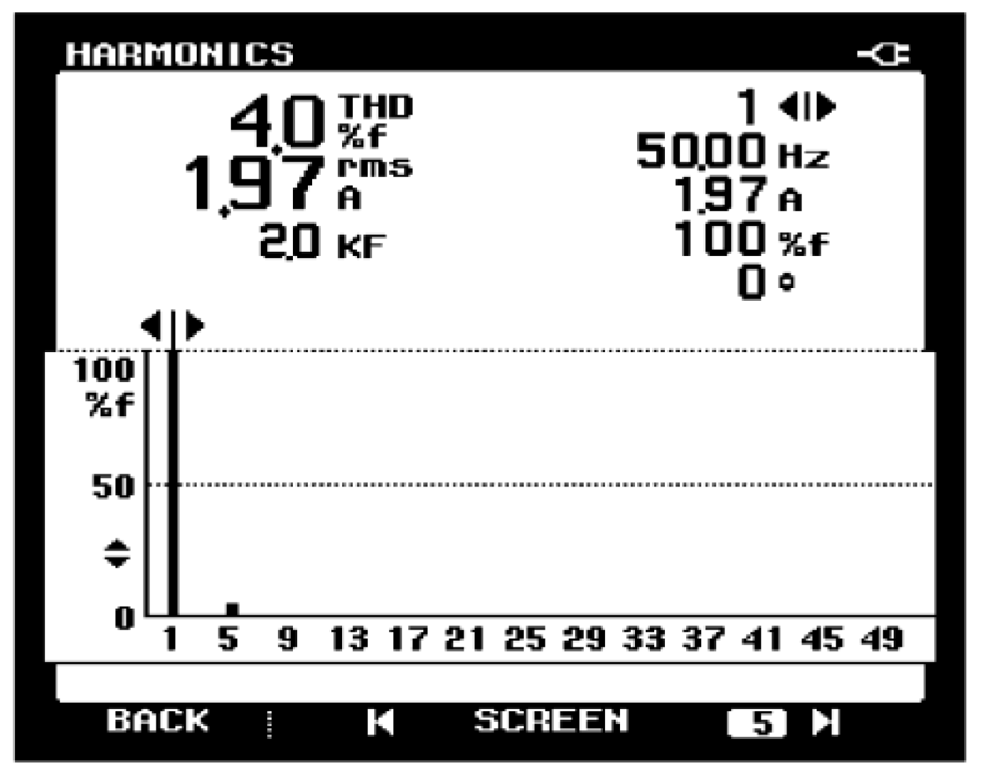
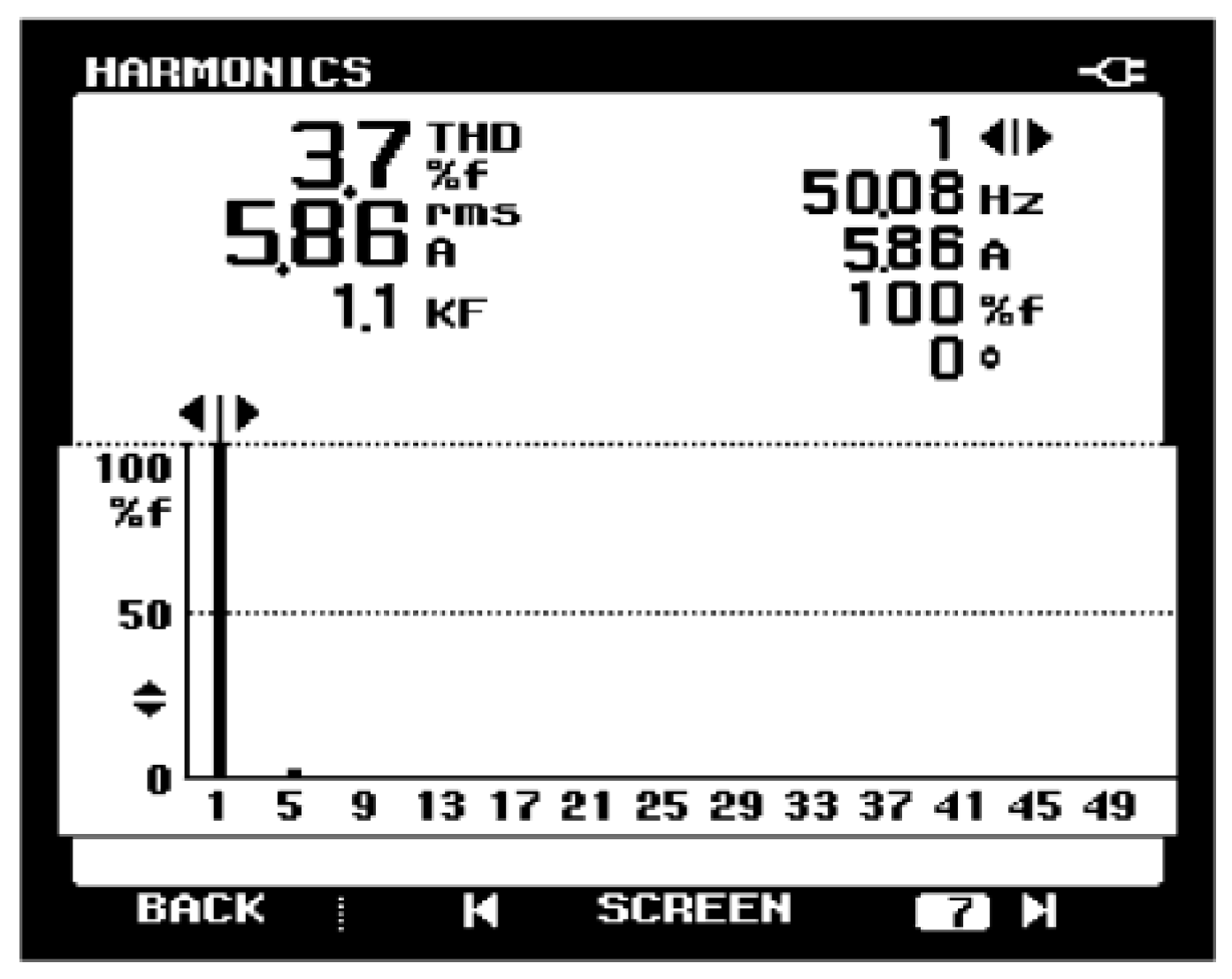
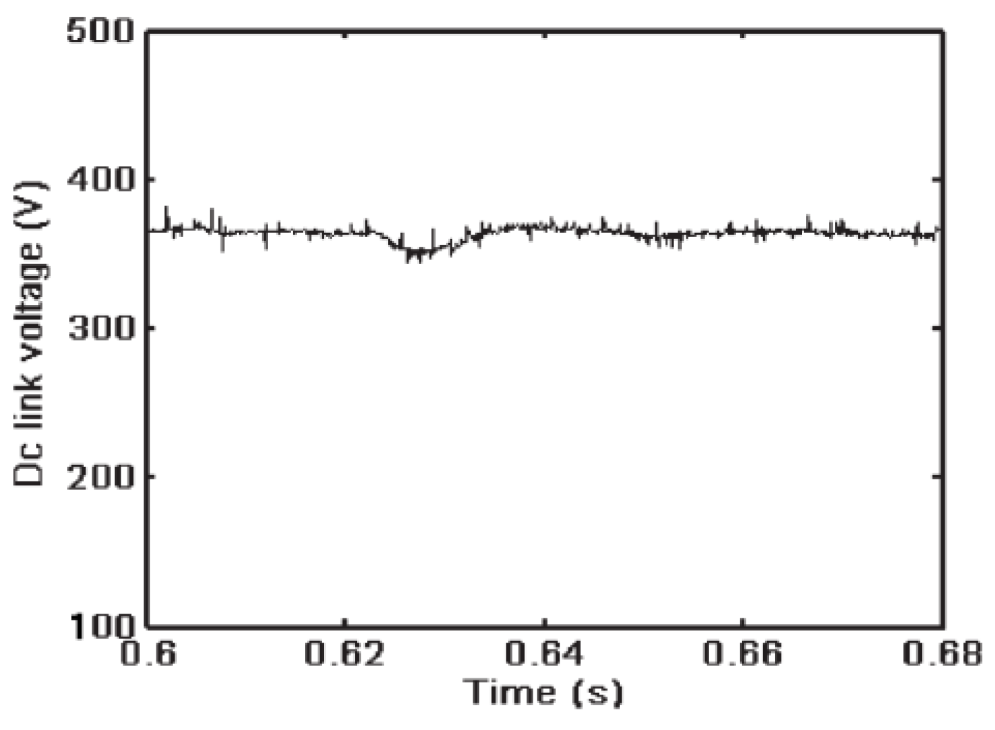
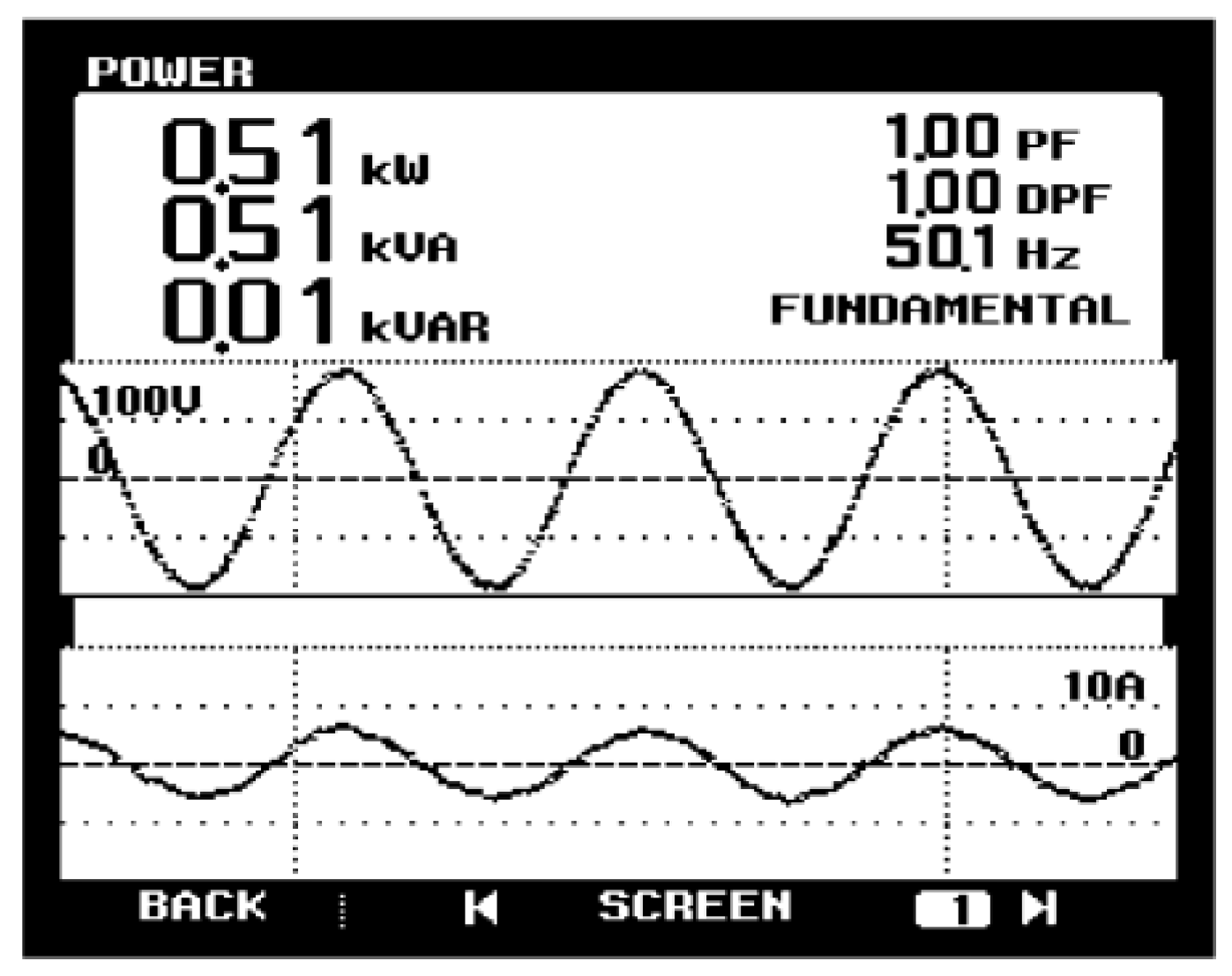
6. Experimental Results and Analysis

The control system is executed utilizing the dSPACE 1102 microprocessor (developed by dSPACE, Paderborn, Germany) and integrated within the MATLAB/Simulink environment. A 1 kW rectifier–inverter prototype is constructed and its properties are thoroughly analyzed and summarized.
Figure 14 and Figure 15 depict the waveforms of the input current and voltage of the rectifier before and after compensation, respectively. These waveforms are obtained using a spectrum analyzer, and numerical explanations accompany them. Additionally, the power factor PF is presented in the upper right corner of both Figure 14 and Figure 15.
Figure 16 and Figure 17 present the spectrum of the experimental input current for both the conventional converter and the proposed converter after undergoing fast Fourier ransform (FFT), respectively.
To further validate the effectiveness of the proposed method, experimental comparisons were conducted using the approach outlined in [26] with the same parameters. The power factor achieved was 0.98, with a THD of 5.0%. This comparison illustrates that the proposed control method effectively enhances the power factor while reducing the total harmonic distortion.
Figure 18 displays the waveforms of the diode current, the source current post-enhancement through the proposed strategy, and the bidirectional switch injection current, all representing the currents of phase-a.
From Figure 19 and Figure 20, it can be determined that for rated output powers of 50% and 150%, the converter demonstrates PF and input current THD values of 0.99 and 4.0%, and 0.99 and 3.7%, respectively.
Figure 21 illustrates the DC link voltage waveform in response to a load disturbance, depicting a momentary transition in the converter’s output power from 50% to 100% of its rated value. The depicted minimal deviation in the DC link voltage output signal attests to the highly commendable response of the proposed control method in regulating the converter amidst sudden load variations.
A comparative analysis was conducted to evaluate the impact of 4 mH and 8 mH input inductances. Figure 22 and Figure 23 present diagrams depicting the input current and voltage of the converter, respectively. In both cases, the results are similar, with only marginal disparities observed. Specifically, the 4 mH case yielded a power factor of 0.99 and a fundamental frequency of 49.9 Hz, while the 8 mH case resulted in a power factor of 1.00 and a fundamental frequency of 50.1 Hz. These findings indicate that integrating the UPF converter with the proposed technique mitigates several shortcomings of conventional converters, such as diminished input power factor resulting from variations in input inductance, output power, and load conditions.

7. Discussion

The comprehensive analysis conducted in this research focused on seven fundamental aspects, providing a thorough assessment of the proposed control technique’s effectiveness. These aspects included THD, PF at various load levels, response to sudden changes in the converter’s output power, and different input inductances. The results of the analysis unequivocally indicate the effectiveness of the proposed control technique across these seven crucial aspects. Specifically, this research highlighted the following key findings:
  • Adjustment of Power Factor: The proposed control technique demonstrated the capability to finely adjust the power factor within a specified target range.
  • Reduction in Current Distortion: The research findings indicated that the proposed control technique effectively reduced the distortion in the power supply current.
  • Improvements in Input Power Factor: The analysis revealed that the input power factor demonstrated significant improvement, even in the presence of fluctuations in input inductance, power, and varying load conditions.
Overall, the comprehensive analysis demonstrated the effectiveness of the proposed control technique in addressing key performance aspects of UPF three-phase rectifiers, thereby showcasing its potential for practical implementation in power electronics systems.

8. Conclusions

In this paper, an improved technique based on steady-state optimization for determining the reference compensation current is proposed. The approach utilizes a multi-objective optimization algorithm to satisfy diverse constraints to enhance the control strategy for the UPF three-phase rectifier. The innovation of the proposed control technique lies in the utilization of a current compensator to filter the load current, ensuring that the compensated power supply current remains within the permissible range of current distortion and imbalance while maintaining a sinusoidal and balanced state. Simultaneously, the load PF can also be adjusted to meet the desired value. Both the simulation and experimental results demonstrate the efficacy of this control technique in reducing power supply current distortion and improving the load power factor.

Author Contributions

Conceptualization, S.Z.; formal analysis, P.W.; investigation, X.L.; methodology, S.Z. and Y.J.; resources, X.L.; software, Y.J.; validation, S.Z. and J.Z.; writing—original draft, Y.J.; writing—review and editing, S.Z. and J.W.; All authors have read and agreed to the published version of the manuscript.

Funding

This research was funded by the S&T Program of Hebei, grant number 22352201D; the Open Project of the Provincial Collaborative Innovation Center of Industrial Energy-Saving and Power Quality Control, Anhui Province, grant number KFKT201504; the Science Foundation of Hebei Normal University, grant number L2023J03.

Data Availability Statement

Data are contained within the article.

Conflicts of Interest

Author Shaoru Zhang and Jielu Zhang were employed by the company Jiangsu Tailong Reducer Co., Ltd. The remaining authors declare that the research was conducted in the absence of any commercial or financial relationships that could be construed as a potential conflict of interest.

References

  1. Zhang, Z.G.; Xu, T.Y.; Xiang, L.P.; Wang, Q. Multi-phase interleaved parallel self-current-sharing high-gain DC/DC converter and its control strategy. J. Electr. Mach. Control 2021, 25, 27–37. [Google Scholar]
  2. Mao, J.; Hong, D.; Ren, R.W.; Li, X.Y. The effect of marine power generation technology on the evolution of energy demand for new energy vehicles. J. Coast. Res. 2020, 103, 1006–1009. [Google Scholar] [CrossRef]
  3. Toledo, O.M.; Oliveira, D.; Diniz, A.S.A.C. Distributed photovoltaic generation and energy storage systems: A review. Renew. Sustain. Energy Rev. 2010, 14, 506–511. [Google Scholar] [CrossRef]
  4. Mao, X.K.; Chen, J.Y.; Zhang, Y.M.; Dong, J.Q. A simple and reconfigurable wireless power transfer system with constant voltage and constant current charging. IEEE Trans. Power Electron. 2022, 37, 4921–4925. [Google Scholar] [CrossRef]
  5. Khan, M.S.U.; Maswood, A.I.; Tariq, M.; Tafti, H.D.; Tripathi, A. Reliability and economic feasibility analysis of parallel unity power factor rectifier for wind turbine system. IET Renew. Power Gener. 2020, 14, 1184–1192. [Google Scholar] [CrossRef]
  6. Chiang, J.H.; Liu, B.D.; Chen, S.M.; Yang, H.T. New power factor correction application for a small wind power system. IEICE Trans. Electron. 2016, E99C, 581–589. [Google Scholar] [CrossRef]
  7. Wimshurst, A.; Willden, R.H.J. Analysis of a tip correction factor for horizontal axis turbines. Wind. Energy 2017, 20, 1515–1528. [Google Scholar] [CrossRef]
  8. Jia, C.R.; Ding, C.; Chen, W.H. Research on the diffusion model of electric vehicle quantity considering individual choice. Energies 2023, 16, 5423. [Google Scholar] [CrossRef]
  9. Gordic, M.; Stamenkovic, D.; Popovic, V.; Muzdeka, S.; Micovic, A. Electric vehicle conversion: Optimisation of parameters the design process. Teh. Vjesn.-Tech. Gaz. 2017, 24, 1213–1219. [Google Scholar]
  10. Dudek, E. The flexibility of domestic electric vehicle charging: The electric nation project. IEEE Power Energy Mag. 2021, 19, 16–27. [Google Scholar] [CrossRef]
  11. Milanés-Montero, M.I.; Gallardo-Lozano, J.; Romero-Cadaval, E.; González-Romera, E. Hall-effect based semi-fast AC on-board charging equipment for electric vehicles. Sensors 2011, 11, 9313–9326. [Google Scholar] [CrossRef]
  12. Caro, L.M.; Ramos, G.; Rauma, K.; Rodriguez, D.F.C.; Martinez, D.M.; Rehtanz, C. State of charge influence on the harmonic distortion from electric vehicle charging. IEEE Trans. Ind. Appl. 2021, 57, 2077–2088. [Google Scholar] [CrossRef]
  13. Zhou, N.C.; Wang, J.J.; Wang, Q.G.; Wei, N.Q. Measurement-based harmonic modeling of an electric vehicle charging station using a three-phase uncontrolled rectifier. IEEE Trans. Smart Grid 2015, 6, 1332–1340. [Google Scholar] [CrossRef]
  14. Hao, T.; Hao, F.; Srdic, S.; Lukic, S. Extreme fast charging of electric vehicles: A technology overview. IEEE Trans. Transp. Electr. 2020, 5, 861–878. [Google Scholar]
  15. Panchanathan, S.; Vishnuram, P.; Rajamanickam, N.; Bajaj, M.; Blazek, V.; Prokop, L.; Misak, S. A comprehensive review of the bidirectional converter topologies for the vehicle-to-grid system. Energies 2023, 16, 2503. [Google Scholar] [CrossRef]
  16. Hsieh, Y.C.; Lin, Z.R.; Chen, M.C.; Hsieh, H.C.; Liu, Y.C.; Chiu, H.J. High-efficiency wireless power transfer system for electric vehicle applications. IEEE Trans. Circuits Syst. II-Express Briefs 2017, 64, 942–946. [Google Scholar] [CrossRef]
  17. Metwly, M.Y.; Abdel-Majeed, M.S.; Abdel-Khalik, A.S.; Torki, M.; Hamdy, R.A.; Hamad, M.S.; Ahmed, S. IoT-based supervisory control of an asymmetrical nine-phase integrated on-board EV battery charger. IEEE Access 2020, 8, 62619–62631. [Google Scholar] [CrossRef]
  18. Sarnago, H.; Lucía, O.; Chhawchharia, S.; Menzi, D.; Kolar, J.W. Novel bidirectional universal 1-phase/3-phase-input unity power factor differential AC/DC converter. Electron. Lett. 2023, 59, 1–3. [Google Scholar] [CrossRef]
  19. Wang, C.; Liu, X.; Li, Z.; Cheng, H.; Chen, T.; Kong, J.Y. Novel high-power triple line-voltage cascaded unity power factor rectifier. J. Power Electron. 2023, 23, 89–101. [Google Scholar] [CrossRef]
  20. Maswood, A.I.; Al-Ammar, E.; Liu, F. Average and hysteresis current-controlled three-phase three-level unity power factor rectifier operation and performance. IET Power Electron. 2011, 4, 752–758. [Google Scholar] [CrossRef]
  21. Mehl, E.L.M.; Barbi, I. An improved high power factor and low cost three-phase rectifier. IEEE Trans. Ind. Appl. 1997, 33, 485–492. [Google Scholar] [CrossRef]
  22. Kolar, J.W.; Zach, F.C. A novel three-phase utility interface minimizing line current harmonics of high power telecommunications rectifiers modules. IEEE Trans. Ind. Electron. 1997, 44, 456–467. [Google Scholar] [CrossRef]
  23. Maswood, A.I.; Liu, F. Unity power factor rectifier-inverter structure operating under unbalanced supply and variable dc bus voltage. IET Power Electron. 2011, 4, 899–907. [Google Scholar] [CrossRef]
  24. Maswood, A.I.; Yusop, A.K.; Rahman, M.A. A novel suppressed-link rectifier-inverter topology with unity power factor. IEEE Trans. Power Electron. 2002, 17, 692–700. [Google Scholar] [CrossRef]
  25. Drofenik, U.; Kolar, J.W. Comparison of not synchronized sawtooth carrier and synchronized triangular carrier phase current control for the VIENNA rectifier. In ISIE’99, Proceedings of the IEEE International Symposium on Industrial Electronics (Cat. No. 99TH8465), Bled, Slovenia, 12–16 July 1999; IEEE: New York, NY, USA, 1999. [Google Scholar]
  26. Maswood, A.I.; Liu, F. A novel unity power factor input stage for AC drive application. IEEE Trans. Power Electron. 2005, 20, 839–846. [Google Scholar] [CrossRef]
  27. Qiao, C.; Smedley, K.M. Three-phase unity-power-factor star-connected switch (VIENNA) rectifier with unified constant-frequency integration control. IEEE Trans. Power Electron. 2003, 18, 952–957. [Google Scholar] [CrossRef]
  28. Liu, F.; Maswood, A.I. A novel variable hysteresis band current control of three-phase three-level unity PF rectifier with constant switching frequency. IEEE Trans. Power Electron. 2006, 21, 1727–1734. [Google Scholar] [CrossRef]
  29. Maswood, A.I.; Liu, F. A unity power factor front-end rectifier with hysteresis current control. IEEE Trans. Energy Convers. 2006, 21, 69–76. [Google Scholar] [CrossRef]
  30. Maswood, A.I.; Liu, F. A unity-power-factor converter using the synchronous-reference-frame-based hysteresis current control. IEEE Trans. Ind. Appl. 2007, 43, 593–599. [Google Scholar] [CrossRef]
  31. IEEE Std. 519-1992; IEEE Recommended Practices and Requirements for Harmonic Control in Electric Power Systems. The Institute of Electrical and Electronics Engineers: New York, NY, USA, 1993.
  32. Chen, D.; Lin, Y.; Xiao, L.; Xu, Z.; Lian, H. A harmonics detection method based on improved comb filter of sliding discrete Fourier for grid-tied inverter. Energy Rep. 2020, 6, 1303–1311. [Google Scholar] [CrossRef]
  33. Optimization Toolbox User’s Guide for Use with Matlab; Version 2; The Math Works, Inc.: Natick, MA, USA, 1999.
Figure 1. UPF rectifier circuit.
Electronics 13 00604 g001
Figure 2. The bidirectional switch structure.
Electronics 13 00604 g002
Figure 3. Voltage and a-phase current isa waveforms.
Electronics 13 00604 g003
Figure 4. Topological stages of the UPF when the phase voltage vsa is 0°–180°. (a) Sa conduction at interval I (0°–30°); (b) Sa disconnection at interval I (0°–30°); (c) Sc conduction at interval II (30°–60°); (d) Sc disconnection at interval II (30°–60°); (e) Sc conduction at interval III (60°, 90°); (f) Sc disconnection at interval III (60°, 90°); (g) Sb conduction at interval IV (90°, 120°); (h) Sb disconnection at interval IV (90°, 120°); (i) Sb conduction at interval V (120°, 150°); (j) Sb disconnection at interval V (120°, 150°); (k) Sa conduction at interval VI (150°, 180°); (l) Sa disconnection at interval VI (150°, 180°).
Electronics 13 00604 g004
Figure 5. Algorithm for generating reference compensation current.
Electronics 13 00604 g005
Figure 6. Control system for the simulated UPF rectifier.
Electronics 13 00604 g006
Figure 7. The proposed control method.
Electronics 13 00604 g007
Figure 8. A frequency converter composed of a unit power factor three-phase rectifier and inverter.
Electronics 13 00604 g008
Figure 9. The waveform and harmonic spectrum of the input phase current of the converter under the proposed control at rated power. (a) The waveform of the input phase current of the converter under the proposed control at rated power. (b) The harmonic spectrum of the input phase current of the converter under the proposed control at rated power.
Electronics 13 00604 g009
Figure 10. The waveform and harmonic spectrum of the input phase current of the traditional converter at rated power. (a) The waveform of the input phase current of the traditional converter at rated power. (b) The harmonic spectrum of the input phase current of the traditional converter at rated power.
Electronics 13 00604 g010
Figure 11. The waveform and harmonic spectrum of input phase current of the proposed method at 50% of the rated power. (a) The waveform of the input phase current of the proposed method at 50% of the rated power. (b) The harmonic spectrum of the input phase current of the proposed method at 50% of the rated power.
Electronics 13 00604 g011
Figure 12. The waveform and harmonic spectrum of the input phase current of the proposed method at 150% of the rated power. (a) The waveform of the input phase current of the proposed method at 150% of the rated power. (b) The harmonic spectrum of the input phase current of the proposed method at 150% of the rated power.
Electronics 13 00604 g012
Figure 13. The converter’s response to load changes. (a) The waveform of the input phase current. (b) DC link voltage.
Electronics 13 00604 g013
Figure 14. The waveforms of voltage and current of an ordinary converter.
Electronics 13 00604 g014
Figure 15. The waveforms of voltage and current of the proposed prototype.
Electronics 13 00604 g015
Figure 16. The spectrum of the conventional converter.
Electronics 13 00604 g016
Figure 17. The spectrum of the proposed converter.
Electronics 13 00604 g017
Figure 18. Diode current, source current, and bidirectional switch injection current of the proposed prototype.
Electronics 13 00604 g018
Figure 19. The spectrum of the proposed prototype at rated output powers of 50%.
Electronics 13 00604 g019
Figure 20. The spectrum of the proposed prototype at rated output powers of 150%.
Electronics 13 00604 g020
Figure 21. The DC link voltage responds to sudden load variations.
Electronics 13 00604 g021
Figure 22. The input current and voltage when the input inductance is 4 mH.
Electronics 13 00604 g022
Figure 23. The input current and voltage when the input inductance is 8 mH.
Electronics 13 00604 g023
Table 1. The prototype parameters.
IndicatorParameter
Rated output power1 kW
Input inductor5 mH
DC link voltage370 V
Input voltage of line-to-line220 V
Disclaimer/Publisher’s Note: The statements, opinions and data contained in all publications are solely those of the individual author(s) and contributor(s) and not of MDPI and/or the editor(s). MDPI and/or the editor(s) disclaim responsibility for any injury to people or property resulting from any ideas, methods, instructions or products referred to in the content.

