Abstract
Compared to single-gate CNTFET, dual-gate structures have better electrostatic control over nanowire conductive channels. However, currently, there is insufficient research on the back-gate effect in a compact model of dual-gate CNTFET. This paper presents an improved dual-gate carbon nanotube field effect transistor (CNTFET) compact model. The functional relationship between the back-gate voltage (Vbg) and threshold voltage (Vth) is derived. And a voltage reference regulation mechanism is adopted so that the back-gate effect can be accurately reflected in the DC transfer characteristics. The influence of gate voltage and drain voltage on transmission probability is analyzed. Meanwhile, the drain current is optimized by modifying the mobility equation. This compact model is built based on Verilog-A hardware language and supports the Hspice simulation tool. Within the supply voltage of 2 V, the simulation results of the proposed compact model are in good agreement with the measurement results. Finally, based on the compact model, an operational amplifier is designed to verify its correctness and feasibility in analog integrated circuits. When the power supply voltage is 1.8 V, and the load capacitance is 2 pF, the gain is 11.8 dB, and the unit-gain-bandwidth (UGB) is 214 kHz, which proves the efficiency of our compact model.
1. Introduction
As a powerful substitute for the CMOS process below 5 nm, the carbon nanotube field effect transistor (CNTFET) has a quasi-one-dimensional structure and an ultra-long mean free path (MFP). While the gate voltage can effectively control the on/off of the transistor, the carrier realizes quasi-ballistic transport in the channel and has very high mobility. Therefore, CNTFET can provide large current transmission capacity in low voltage environments, offering a solution for the implementation of nano-scale analog/logic circuits.
As a new nano device, CNTFET avoids most of the basic limitations of traditional silicon devices. Its structural and electronic advantages are shown in the following aspects: (1) Easy integration with high-k dielectric materials. All carbon atoms in CNTFET bond with each other via sp2 hybridization, which makes it possible to integrate with high-k dielectric materials so as to effectively reduce the leakage current in the channel. At the same time, it also reduces the impurity diffusion of the gate dielectric layer and avoids the diffusion of a large number of impurities from gate to substrate, which may change the device threshold voltage and worsen the device’s performance; (2) High mobility. Single-walled CNTFET can be regarded as a piece of graphene, and the electrons in CNTFET are confined in the atomic plane of graphene. Due to the quasi-one-dimensional structure of CNTFET, the movement of electrons in nanotubes is strictly limited. Electrons can only move freely along the axis of the tube without scattering. For the carriers in CNTFET, only forward scattering and backscattering due to their interaction can occur. Moreover, CNTFETs have ultra-long MFP ~(1 μm) of elastic scattering, which means that carriers behave as ballistic or quasi-ballistic transport in the channel. So, their mobility is much higher than that of the known MOSFETs; (3) High current capacity. The current capacity of CNTFET is about 3 orders of magnitude higher than the maximum current capacity of copper, and there will be no performance degradation during operation at high temperatures. The excellent carrier transport and conduction characteristics make CNTFET suitable for interconnection and electronic applications of nanodevices; (4) Better conductive channel control. The three (or four) terminal device consists of a semiconductor nanotube, which acts as a conductive channel and bridges the source and drain. The device is turned on or off by gate electrostatic control. The quasi-one-dimensional structure can provide better gate electrostatic control in the channel region than 3D and 2D device (such as FinFET and FD-SOI) structures.
At present, CNTFET has made great progress in material, device, and small-scale logic IC. However, as a bridge between circuit design and process integration, the compact model is still a missing link in the research field of CNTFET. A compact model is necessary for large-scale simulation and verification of CNTFET integrated circuits. Most of the existing compact models are based on single-gate CNTFET [1,2,3,4,5,6,7,8,9]. In 2002, J. Guo et al. proposed the first CNTFET compact model with the numerical analysis method [10]. With a large number of integral functions for calculation, when embedding commercial simulators such as Hspice for simulation, it operates very slowly, and the practicability is poor. A. Raychowdhury et al. improved the model simulation time significantly by using the polynomial fitting method [11]. However, this method does not fully map the physical meaning of the device. In order to further simplify the above two models, the model reported by C. Dwyer et al. uses a simple coaxial or planar gate CNTFET structure [12]. The compact model proposed by the research team of the University of Tsukuba integrates multiple lumped static gate capacitors [13] and assumes that CNTFET has an ideal ballistic transport channel. However, these simplifications lead to errors in evaluating the transient response of transistors and the dynamic performance of devices. In most research achievements, the back gate is usually used as a common substrate. These compact models ignore the modulation effect of the back gate on the conductive channel, thus introducing errors in the DC characteristics of CNTFET. However, in practice, dual-gate CNTFET can construct n-type or p-type transistors according to different back-gate bias voltages. And the back gate provides an additional degree of freedom, which can regulate the conductive channel, and then affect the transmission current and threshold voltage. To date, only a few research institutions, such as IBM and Stanford University, have proposed the compact model of dual-gate CNTFET. The IBM model believes that although the back gate has some influence on drain current Ion, the source depletion effect appears quickly under a small back-gate voltage, and the conduction current is mainly controlled by the front gate. Therefore, the front gate screens the influence of the back gate on the internal conductive channel [14]. The dual-gate CNTFET compact model proposed in Ref. [15] measures Ids at different front-gate voltages (VFG), and it is observed that the back gate will cause the change in threshold voltage. This compact model only shows the back-gate effect and does not conduct a deep investigation of this effect. But it still provides experimental basis and exploration ideas for follow-up research. Ref. [16] has further studied dual-gate CNTFET. When constructing a compact model, the conductive channel is divided into three regions: source access, inner part, and drain access. It is considered that there is a strong coupling effect between the front gate and the back gate. The back gate adjusts ambipolarity by controlling the source access and drain access areas.
Based on experimental results, the above compact models only show the back-gate effect and does not analyze its specific mechanism. Therefore, an improved compact model with a back-gate effect is proposed in this paper. In this model, the principle of the back-gate effect is analyzed in detail, and the relationship between the back-gate voltage and the threshold voltage is derived via accurate calculation and numerical fitting. At the same time, in order to further expand its application, the influence of gate voltage and drain voltage on transmission probability is also analyzed, which improves the calculation accuracy of channel current. Comparing the simulation results with the measurement results, they have good consistency. Finally, via the simulation of the operational amplifier, the practicability of the model in a circuit simulation environment is verified.
2. Improved Dual-Gate CNTFET Model
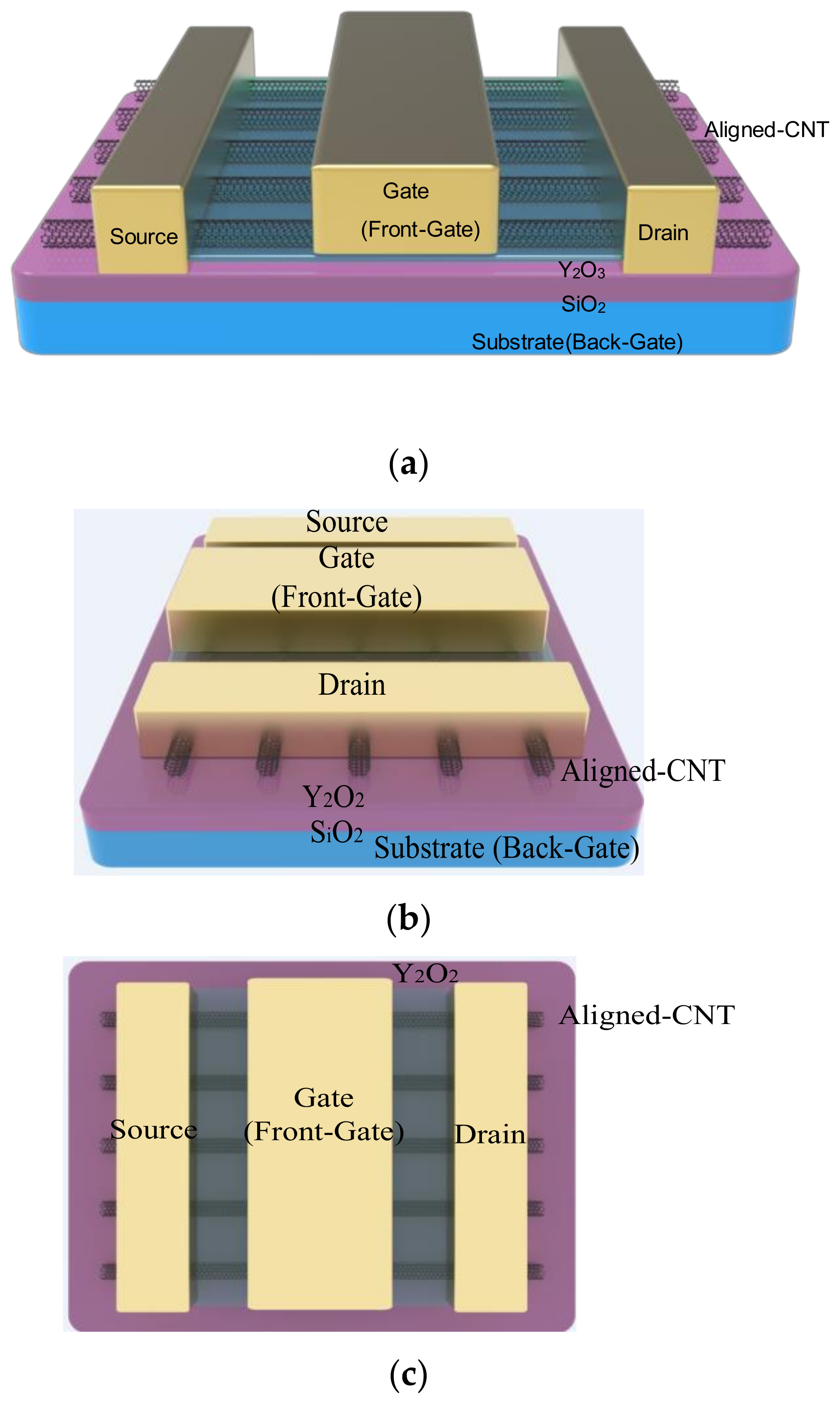
In this paper, the dual-gate CNTFET structure similar to Ref. [17] is used, as shown in Figure 1. The heavily doped substrate is also used as the back-gate terminal.

Figure 1.
Dual-gate CNTFET structure: (a) front view; (b) side view; (c) top view.
2.1. Back-Gate Effect
In the following discussion, we use the symbol to denote the surface potential (in units of volts) and the symbol ϕ to denote the corresponding energy level (in units of electronvolts). In CNTFET, x is the direction perpendicular to the surface, and the surface energy level can be expressed as
q is the electron charge, NA is the substrate doping concentration and is the dielectric constant of silicon material. By integrating (1), it can be obtained that the electric field distribution in the silicon film is
, is the surface potential of the front gate and back gate, respectively. is the thickness of silicon film. When x = 0, that is, on the surface, the electric field of the front-gate surface is expressed as
According to Gauss law, the voltage drop on the oxide layer at the front gate can be obtained as
is the fixed charge in gate oxide, is the inversion-layer charge, and is the gate oxide capacitance per unit area. It is also deduced that the voltage drop on the oxide layer at the back gate is
is the fixed charge in the back-gate oxide layer, and is the inversion-layer charge on the back gate. Therefore, the front-gate voltage and the back-gate voltage can be obtained as follows:
and represent the work function difference between the front gate, the back gate, and the substrate. By combining Equations (3), (4), (6), and (7), we can obtain the front-gate and the back-gate voltage, and the surface potential as
where , is the depletion-layer charge.
When CNTFET is inverted, it is considered that is the threshold voltage at this time. Then, ( is the Fermi potential) and is put into Equation (8)
There is no inversion charge at the back gate ().
Equation (11) is substituted into Equation (10) to obtain the following:
It can be seen that the threshold voltage of CNTFET is directly affected by the back-gate voltage.
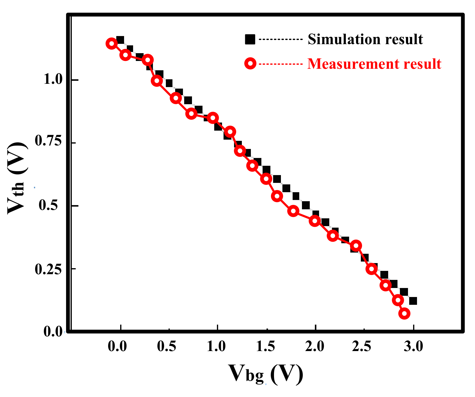
When the drain voltage is small (e.g., = 0.1 v), the gate voltage when the drain current is 0.1 μA is set as the threshold voltage (). The proposed compact model is simulated and compared with the device measurement results. As shown in Figure 2, the model simulation results have a high degree of fit with the measurement results, which verifies the correctness of the inference. The maximum error margin is about 4% of the full range.

Figure 2.
Relationship between threshold voltage and back-gate voltage.
Further analysis shows that the surface potential increases with the increase in the back-gate voltage, and decreases with the increase in the back-gate voltage. Meanwhile, the relationship between the front-gate voltage variation and the surface potential variation is double. Therefore, the change in is approximately twice that of surface potential variation . This is because the increase in the gate voltage makes the energy band bend downward, and the surface potential increases. Then, the electron concentration at the surface increases, and the current increases. When the surface potential increases, the applied voltage required to reach the fixed current value decreases, and decreases. Therefore, the trend of surface potential and changing with the back-gate voltage is the opposite. The back-gate voltage will affect the current by affecting the change in surface potential, so it is very important for the model to correctly reflect the influence of the back gate on the current.
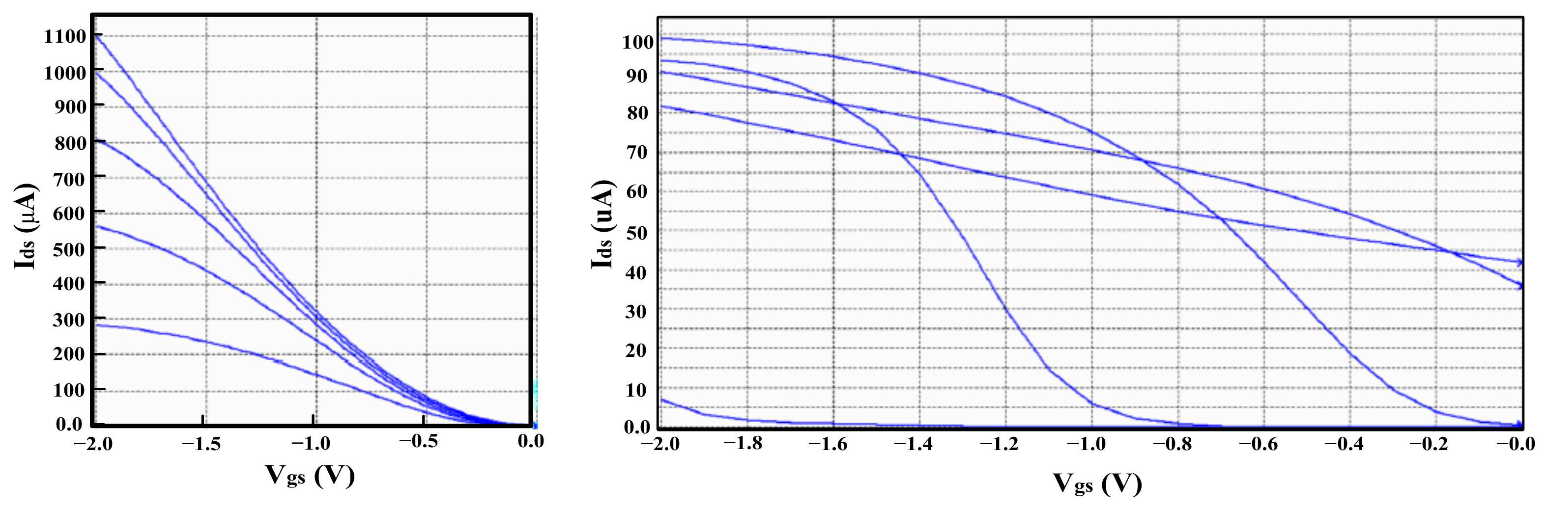
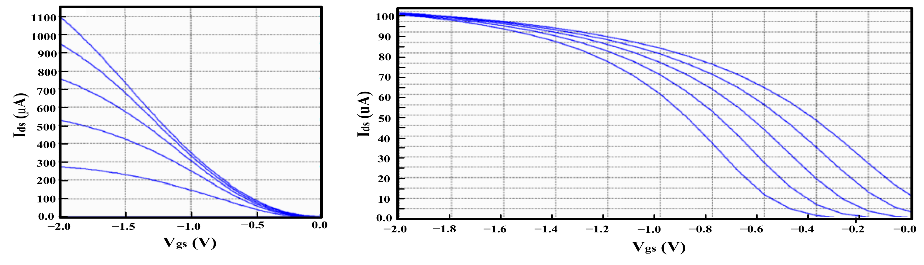
Since the back gate of CNTFET is used as a substrate, the back gate is connected to the power supply by default during the parameter extraction of the p-CNTFET model. Therefore, there will be a voltage difference between the back gate and its source. And the influence of back-gate voltage must be correctly reflected in the model. As shown in Figure 3, according to the simulation results, the transfer characteristic of the p-CNTFET model is inconsistent when the source and back gate are connected with different voltages. The reason for this is that the terminal voltage in the model adopts absolute voltage, which leads to an error in the voltage input to the model and the wrong result. Therefore, it is optimized to deduct a voltage from the input voltage in the model so that the transfer characteristic of the output when the source and back gate are connected with different reference voltages is consistent, as shown in Figure 4. Then, the back-gate voltage effect can be reflected in the transfer characteristic. The back-gate voltage also affects the threshold voltage of CNTFET. This mechanism is similar to MOSFET, where changes in threshold voltage can cause a certain degree of nonlinearity in the transfer characteristic curve. Therefore, even after optimization, there is still about 1% nonlinearity in the transfer characteristic curve in Figure 4 [18]. Because the currently developed compact models are mainly aimed at Hspice simulation applications, all results in this paper are based on Hspice simulation. Since the CNTFET’s maximum supply voltage is 2 V, Vgs is swept from 2 to 0 V in Figure 3, Figure 4, Figure 5, Figure 6, Figure 7 and Figure 8. From Figure 3 and Figure 4, it can be seen that when Vgs is greater than 1.2 V, CNTFET is saturated. When the Vgs is less than 1.2 V, CNTFET enters the linear working region.
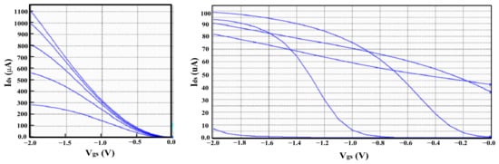
Figure 3.
Transfer characteristics before optimization.
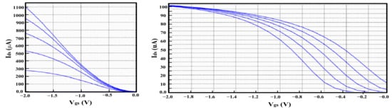
Figure 4.
Transfer characteristics after optimization.
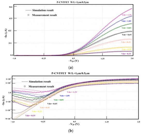
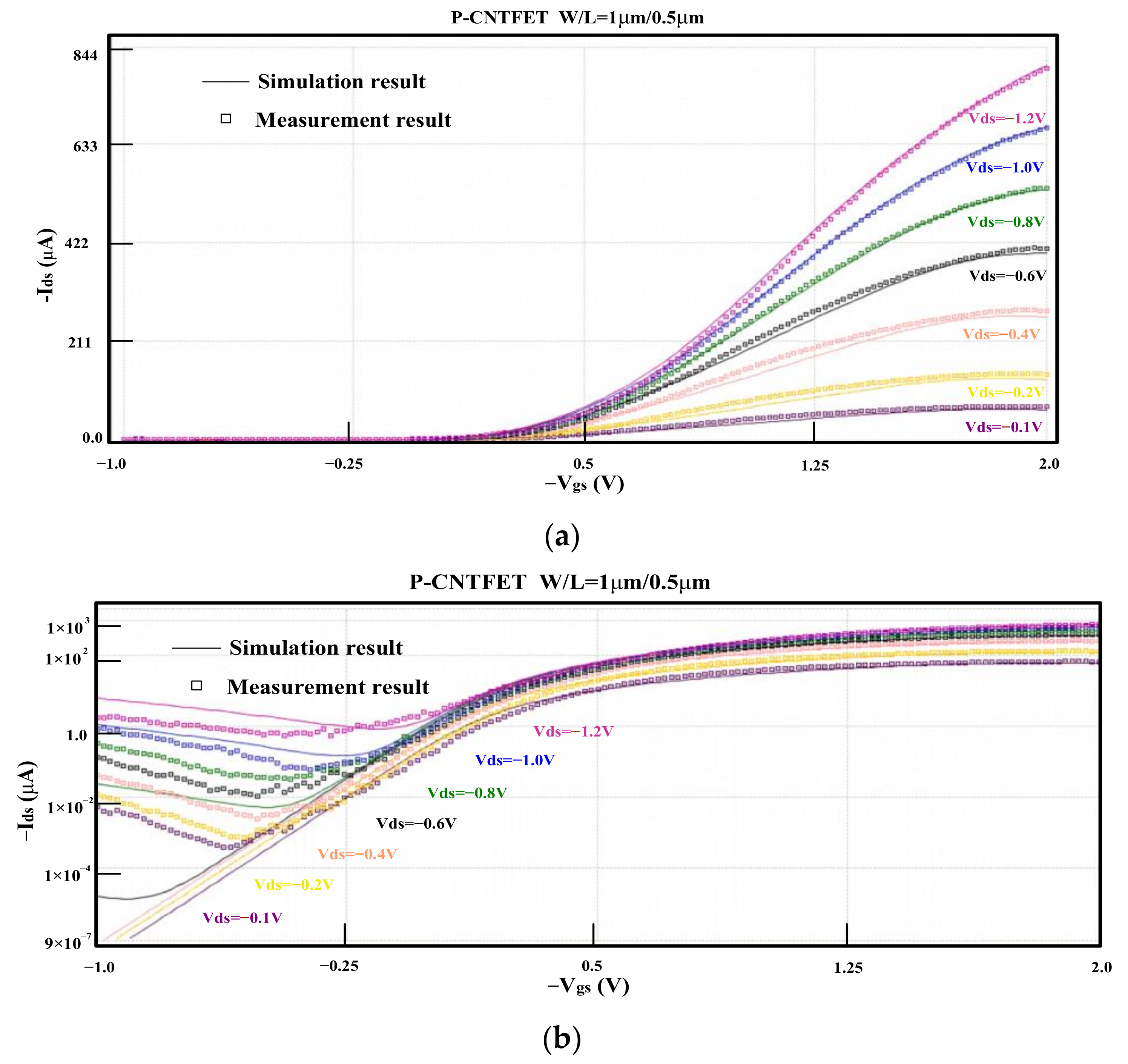
Figure 5.
The 500 nm P-CNTFET fitting results: (a) linear coordinate; (b) logarithmic coordinate.
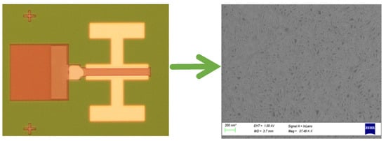
Figure 6.
CNTFET SEM.
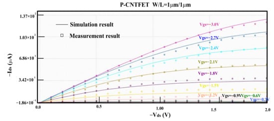
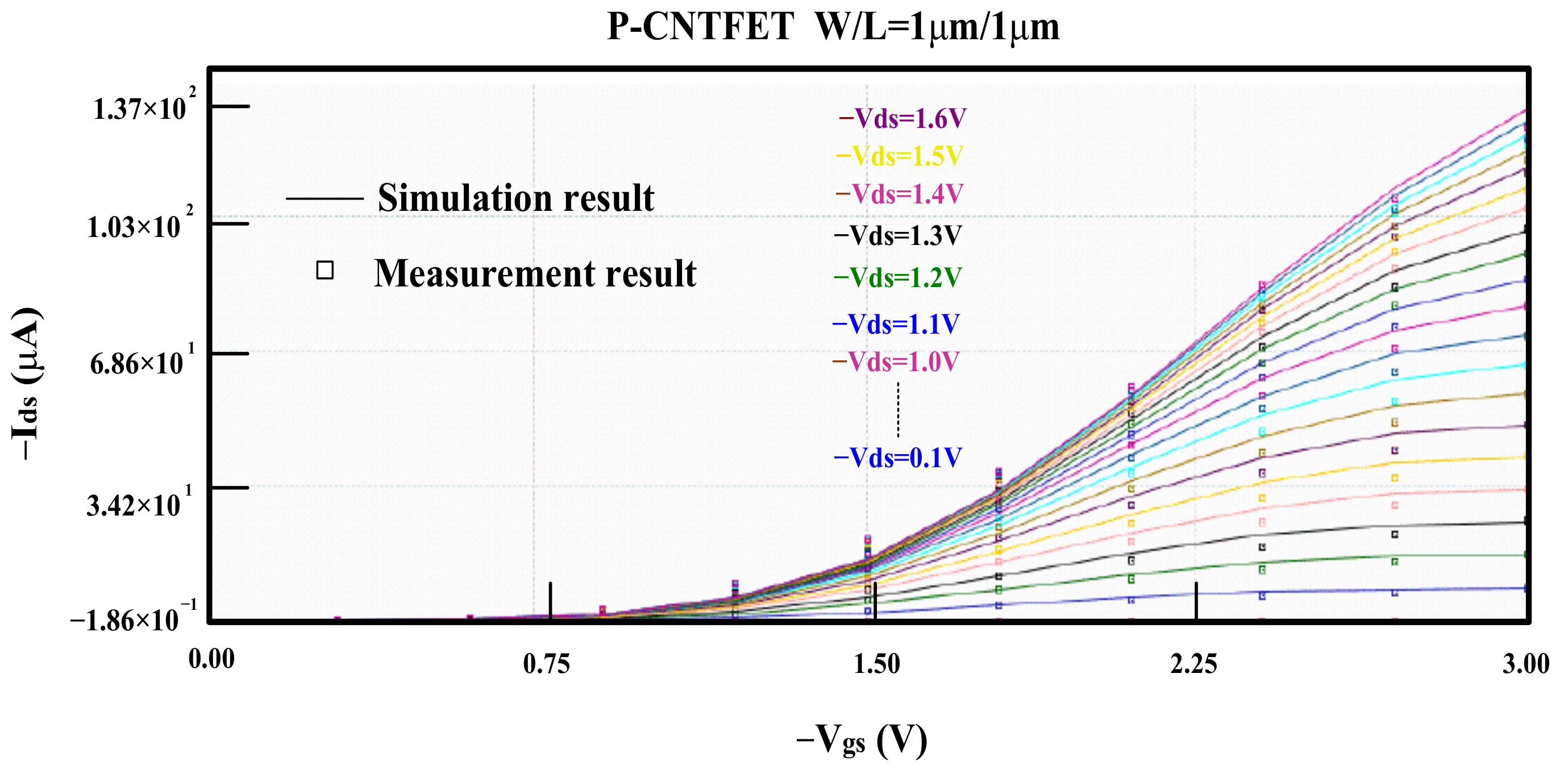
Figure 7.
P-CNTFET output characteristics.
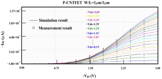
Figure 8.
P-CNTFET transfer characteristics.
2.2. Transmission Probability Optimization
Since the scattering caused by defects is suppressed in CNTFET, the main source of scattering is considered to be phonons, especially at high temperatures. There are many phonon modes in CNTFET, and phonon scattering is an inelastic scattering process. There are only three kinds of electron–phonon backscattering in CNTFET. The first is the scattering of low-energy acoustic phonons, which involves small changes in momentum and energy. The other two scattering processes are due to optical phonons and Brillouin boundary phonons, which require large energy changes (150–180 meV) and large momentum changes, respectively. Phonon scattering involves the emission or absorption of phonons by moving charge carriers. When Vds is small, acoustic phonon scattering is the only scattering process that occurs because electrons do not have enough energy to interact with high-energy phonons. In this case, the resistance is inversely proportional to the temperature because the scattering probability is determined by the number of available phonons [19]. The direct effect of phonon scattering is to reduce the transmission probability and the transmission current in the channel.
In CNTFET, the carrier injection depends on the transmission probability and the drain and source voltages. There are two main ways for electrons to pass through the barrier from source, drain to channel: thermal excitation and tunneling [20]. In an ideal scenario, ignoring the influence of nonideal effects such as scattering, tunneling, and traps, we believe that all charge carriers can be transferred from the source to the drain, which means that the accumulated charge in the drain is equal to the charge in the source. Therefore, we set T(E) to 1. For one-dimensional systems, the Landauer–Buttiker approximation can be used to calculate the current from drain to source [15] as follows:
T(E) is the coefficient related to energy transmission, is the Fermi–Dirac distribution, E is energy, and and are the Fermi energy of source and drain, respectively.
For a ballistic transmission system, as long as the energy of the electron is higher than the top of the potential barrier in the channel region, it can be directly transmitted to the drain due to thermal motion. At this time, the transmission probability T(E) of the carrier is 1, and its conductivity is controlled by drain and gate voltage. However, the channel region of the device is not completely ballistic, and the current is far lower than the current predicted by the ballistic model. The transmission probability of the carrier in non-ballistic transmission depends on the channel scattering mechanism. Both phonon scattering and optical phonon scattering depend on carrier energy.
With the increase in gate voltage, the surface potential of CNTFET increases, and the energy band of the channel region decreases. The Fermi energy of carriers along the +k and -k directions are the source and drain Fermi energy, respectively. All +k states are filled according to the Fermi energy at source, and all -k states are filled according to the Fermi energy at drain [21]. Since the Fermi energy in the source and drain region remains unchanged, the energy difference between the substrate and the Fermi energy will decrease with the decrease in the energy band in the channel region. With the increase in the Fermi–Dirac distribution function, the probability that the substrate is occupied increases, so the probability that the substrate is empty decreases. Therefore, with the increase in gate voltage, the number of empty substates where electron transition can occur becomes less, the MFP of scattering increases, and the carrier transmission probability increases.
The drain voltage also affects the scattering. With the increase in drain voltage, the Fermi energy of the drain decreases. Therefore, the Fermi distribution function decreases, the number of states in which the electron transition can occur is empty increases, the scattering MFP decreases, and the electron transmission probability from drain to source decreases [22,23]. For current Ids, it is the drain to source current minus the source to drain current; For electrons, it is the source to drain electrons minus drain to source electrons. For the drain electrons, the Fermi distribution function is smaller than the source when the drain voltage is applied, and the Fermi distribution function will continue to decrease with the increase in drain voltage. Therefore, when drain voltage increases, the transmission probability and Fermi distribution function of electrons from drain to source will decrease, and the total current will increase. Therefore, the influence of drain voltage on scattering can be expressed indirectly by the Fermi distribution function.
So, the transmission probability is related to gate voltage and increases with the increase in gate voltage. The Fermi distribution function of the source and drain region is also related to gate voltage and gradually increases with the increase in gate voltage. In order to solve these problems, the Fermi distribution function of source and drain and the transmission probability of source and drain carriers need to be related to gate voltage, taking the mobility model in the BSIM model as a reference [24].
Three parameters, coeffvg0, coeffvg1, and coeffvg2, are added to the model so that the mobility in the model is related to the Fermi distribution function and gate voltage, thus indirectly reflecting the current transmission probability. We have not yet completed our research on this mechanism. Currently, we can only use these three coefficients to fit the simulation results of the compact model with the measured results. The specific adding methods are as follows:
tempt = coeffvg0/(1 + coeffvg1 × (v_vg − v_vs) + coeffvg2 × (v_vg − v_vs) × (v_vg − v_vs));
current_sub11 = (T11 × fermi_s11 − T11_0 × fermi_d11) × Coeff_J11;
current_sub11 = (T11 × fermi_s11 − T11_0 × fermi_d11) × Coeff_J11;
By adjusting coeffvg0, coeffvg1, and coeffvg2, the current value in the right area of the simulation curve of the Ids-Vgs-Vds model can be modified, and the rise and change in the simulation curve can be adjusted. As shown in Figure 5, the model simulation and device measurement results are compared, and the fitting degree of the two is good. However, in linear coordinates, the current value in the negative voltage region is particularly small and has not been characterized. Essentially, the two graphs are consistent.
3. Experimental Results and Circuit Implementation
The CNTFET is manufactured in a similar process to MOSFET; SEM photos are shown in Figure 6. This compact model is built based on Verilog-A hardware language, which describes the physical characteristics of CNTFET. The CNTFET-based circuit is simulated using the Hspice tool. The main parameters in the compact model are shown in Table 1, and each parameter has a clear physical meaning.

Table 1.
Model parameter definition.
The above parameters are imported into the model. The process parameters of p-CNTFET are the length and width at both 1 μm. There are about 200 carbon tubes every 1 μm wide, and the chirality of CNTFET is (14, 7). According to the diameter equation, the diameter can be obtained:
The coupling capacitance between the channel and back gate can be calculated according to the buried-oxide thickness. The parameter pitch can be obtained when there are 200 carbon tubes in 1 μm width. The number of carbon tubes can be determined according to the gate width and the density of carbon tubes. Let tubes = W/(1 × 10−6 × 200). The threshold voltage of the curve is adjusted by changing the flat band voltage Vfbp. The increase in Lss and Ldd will increase the resistance in the source/drain region and reduce the overall current value on the right side of the Ids-Vgs simulation curve; Ccsd and CoupleRatio will affect the electrode-induced charge in the channel, thus affecting the solution of surface potential and tcurrent. With the increase in Ccsd, the surface potential decreases, so the current decreases. CoupleRatio will change the influence of drain voltage on surface potential.
The proposed compact model is simulated. The output characteristic of p-CNTFET is shown in Figure 7, and the transfer characteristic is shown in Figure 8. The results show that the simulation results are in good agreement with the test results, which proves the effectiveness of the compact model.
In analog integrated circuit design, the compact model determines the accuracy of circuit simulation. Based on the proposed dual-gate compact model, an operational amplifier is designed. As shown in Figure 9, the back gate of the input differential transistor p-CNTFET is connected to a power supply to reduce the threshold voltage and increase transconductance. When the power supply voltage is 1.8 V, and the load capacitance is 2 pF, the AC small-signal simulation is carried out. The simulation results show that the gain is 11.8 dB, and the unit-gain-bandwidth (UGB) is 214 kHz. It has the basic amplifier function, which verifies the feasibility of the compact model and its convergence in the spice simulator.
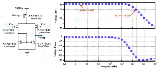
Figure 9.
CNTFET-based operational amplifier and its output AC characteristics.
As shown in Table 2, based on other research achievements, the compact model proposed in this paper is aimed at the 90 nm CNTFET process and provides a relatively complete description of the back-gate effect and its impact on transport probability, which is constructed using analysis methods with good simulation convergence.
Table 2.
Performance comparison of CNTFET compact model.
4. Conclusions
In order to characterize dual-gate CNTFET, an improved compact model is proposed in this paper. The compact model mainly analyzes the influence of back-gate voltage on threshold voltage and deduces the relationship between them. At the same time, based on the influence of phonon scattering on carrier transmission, the effect of gate voltage and drain voltage on transmission probability is analyzed, and the carrier mobility in the model is modified to fit the device current more accurately. In order to more accurately characterize the model, three fitting parameters were added to the mobility formula based on the CNTFET test results. The output characteristics and transfer characteristics of CNTFET are simulated and tested to verify the accuracy of the model. This compact model includes the main CNTFET parameters, such as Channel length, Tox, and so on. Finally, via the simulation of the operational amplifier, which shows a gain of 11.8 dB and UGB of 214 kHz. The convergence and simulation feasibility of the model in an analog integrated circuit design environment are verified.
Author Contributions
Conceptualization, Z.C. and C.C.; software simulation and parameter optimization, Z.C. and J.J.; data processing, Y.Z.; writing—original draft preparation, Z.C. and J.J.; writing—review and editing, Z.C. and C.C.; supervision, C.C. and J.J. All authors have read and agreed to the published version of the manuscript.
Funding
This research was funded by the Natural Science Foundation of Fujian Province (No. 2023H0052), Major science and technology projects of Xiamen (3502Z20221022), and Jihua Laboratory (project no. 2021B0301030003-03).
Data Availability Statement
All the data are reported/cited in the paper.
Conflicts of Interest
The authors declare no conflicts of interest.
References
- Solomon, P.M. Contact Resistance to a one-dimensional quasi-ballistic nanotube/wire. IEEE Electron. Device Lett. 2011, 32, 246–247. [Google Scholar] [CrossRef]
- Knoch, J.; Appenzeller, J. Tunneiling phenomena in carbon nanotube field-effect transistor. Phys. Status Solidi A 2008, 205, 679–694. [Google Scholar] [CrossRef]
- Ossaimee, M.I.; Gamal, S.H.; Kirah, K.A.; Omar, O.A. Ballistic transport in Schottky barrier carbon nanotube FETs. Electron. Lett. 2008, 44, 336–337. [Google Scholar] [CrossRef]
- Kazmierski, T.J.; Zhou, D.; Al-Hashimi, B.M.; Ashburn, P. Numerically efficient modeling of CNT transistor with ballistic and nonballistic effect for circuit simulation. IEEE Trans. Nanotechnol. 2010, 9, 99–107. [Google Scholar] [CrossRef]
- Bejenari, I.; Schröter, M. Analytical drain current model of 1-D ballistic schottky-barrier transistor. IEEE Trans. Electron. Devices 2017, 64, 3904–3911. [Google Scholar] [CrossRef]
- Najari, M.; Fregonese, S.; Maneux, C.; Mnif, H.; Masmoudi, N.; Zimmer, T. Schottky barrier carbon nanotube transistor: Compact modeling, scaling study, and circuit design applications. IEEE Trans. Electron. Devices 2011, 58, 195–205. [Google Scholar] [CrossRef]
- Gelao, G.; Marani, R.; Diana, R.; Perri, A.G. A Semiempirical SPICE model for n-type conventional CNTFETs. IEEE Trans. Nanotechnol. 2010, 10, 506–512. [Google Scholar] [CrossRef]
- Wei, L.; Frank, D.J.; Chang, L.; Wong, H.S.P. Noniterative Compact Modeling for Intrinsic Carbon-Nanotube FETs: Quantum Capacitance and Ballistic Transport. IEEE Trans. Electron. Devices 2011, 58, 2456–2465. [Google Scholar] [CrossRef]
- Luo, J.; Wei, L.; Lee, C.S.; Franklin, A.D.; Guan, X.; Pop, E.; Antoniadis, D.A.; Wong, H.S.P. Compact Model for Carbon Nanotube Field-Effect Transistors Including Nonidealities and Calibrated with Experimental Data Down to 9-nm Gate Length. IEEE Trans. Electron. Devices 2013, 60, 1834–1843. [Google Scholar] [CrossRef]
- Guo, J.; Lundstrom, M.; Datta, S. Performance Projections for Ballistic Carbon Nanotube Field-Effect Transistors. Appl. Phys. Lett. 2002, 80, 3192–3194. [Google Scholar] [CrossRef]
- Raychowdhury, A.; Mukhopadhyay, S.; Roy, K. A Circuit-Compatible Model of Ballistic Carbon Nanotube Field-Effect Transistors. IEEE Trans. Comput. Des. Integr. Circuits Syst. 2004, 23, 1411–1420. [Google Scholar] [CrossRef]
- Dwyer, C.; Cheung, M.; Sorin, D. Semi-empirical SPICE models for carbon nanotube FET logic. In Proceedings of the 4th IEEE Conference on Nanotechnology, Munich, Germany, 16–19 August 2004. [Google Scholar]
- Natori, K.; Kimura, Y.; Shimizu, T. Characteristics of a Carbon Nanotube Field-Effect Transistor Analyzed as a Ballistic Nanowire Field-Effect Transistor. J. Appl. Phys. 2005, 97, 034306. [Google Scholar] [CrossRef]
- Lin, Y.; Appenzeller, J.; Knoch, J.; Avouris, P. High-performance carbon nanotube field-effect transistor with tunable polarities. IEEE Trans. Nanotechnol. 2005, 4, 481–489. [Google Scholar] [CrossRef]
- Frégonèse, S.; Maneux, C.; Zimmer, T. A Compact Model for Dual-Gate One-Dimensional FET: Application to Carbon-Nanotube FETs. IEEE Trans. Electron. Devices 2011, 58, 206–215. [Google Scholar] [CrossRef]
- Deng, J.; Wong, H.-S.P. A Compact SPICE Model for Carbon-Nanotube Field-Effect Transistors Including Nonidealities and Its Application—Part I: Model of the Intrinsic Channel Region. IEEE Trans. Electron. Devices 2007, 54, 3186–3194. [Google Scholar] [CrossRef]
- Deng, J.; Wong, H.-S.P. A Compact SPICE Model for Carbon-Nanotube Field-Effect Transistors Including Nonidealities and Its Application—Part II: Full Device Model and Circuit Performance Benchmarking. IEEE Trans. Electron. Devices 2007, 54, 3195–3205. [Google Scholar] [CrossRef]
- Bucolo, M.; Buscarino, A.; Famoso, C.; Fortuna, L.; Gagliano, S. Imperfections in Integrated Devices Allow the Emergence of Unexpected Strange Attractors in Electronic Circuits. IEEE Access 2021, 9, 29573–29583. [Google Scholar] [CrossRef]
- Patil, N.; Lin, A.; Zhang, J.; Wei, H.; Anderson, K.; Wong, H.S.P.; Mitra, S. Scalable Carbon Nanotube Computational and Storage Circuits Immune to Metallic and Mispositioned Carbon Nanotubes. IEEE Trans. Nanotechnol. 2011, 10, 744–750. [Google Scholar] [CrossRef]
- Zhang, Y.; Yang, Y.; Yang, T.; Zhang, Y. A Compact Physical Drain Current Model of Multitube Carbon Nanotube Field Effect Transistor Including Diameter Dispersion Effects. IEEE Trans. Electron. Devices 2021, 68, 6571–6579. [Google Scholar] [CrossRef]
- Rahman, A.; Guo, J.; Datta, S.; Lundstrom, M.S. Theory of ballistic nanotransistors. IEEE Trans. Electron. Devices 2003, 50, 1853–1864. [Google Scholar] [CrossRef]
- Michetti, P.; Iannaccone, G. Analytical model of one-dimensional carbon-based schottky-barrier transistors. IEEE Trans. Electron. Devices 2010, 57, 1616–1627. [Google Scholar] [CrossRef]
- Zhu, G.; Zhou, X.; Lee, T.S.; Ang, L.K.; See, G.H.; Lin, S.; Chin, Y.K.; Pey, K.L. A Compact Model for Undoped Silicon-Nanowire MOSFETs with Schottky-barrier source drain. IEEE Trans. Electron. Devices 2009, 56, 1100–1109. [Google Scholar] [CrossRef]
- BSIM Group. BSIMSOIv4.4 MOSFET MODEL Users’ Manual; University of California: Berkeley, CA, USA, 2010. [Google Scholar]


Disclaimer/Publisher’s Note: The statements, opinions and data contained in all publications are solely those of the individual author(s) and contributor(s) and not of MDPI and/or the editor(s). MDPI and/or the editor(s) disclaim responsibility for any injury to people or property resulting from any ideas, methods, instructions or products referred to in the content. |
© 2024 by the authors. Licensee MDPI, Basel, Switzerland. This article is an open access article distributed under the terms and conditions of the Creative Commons Attribution (CC BY) license (https://creativecommons.org/licenses/by/4.0/).