

Liquid Crystal-Filled 60 GHz Coaxially Structured Phase Shifter Design and Simulation with Enhanced Figure of Merit by Novel Permittivity-Dependent Impedance Matching

Abstract
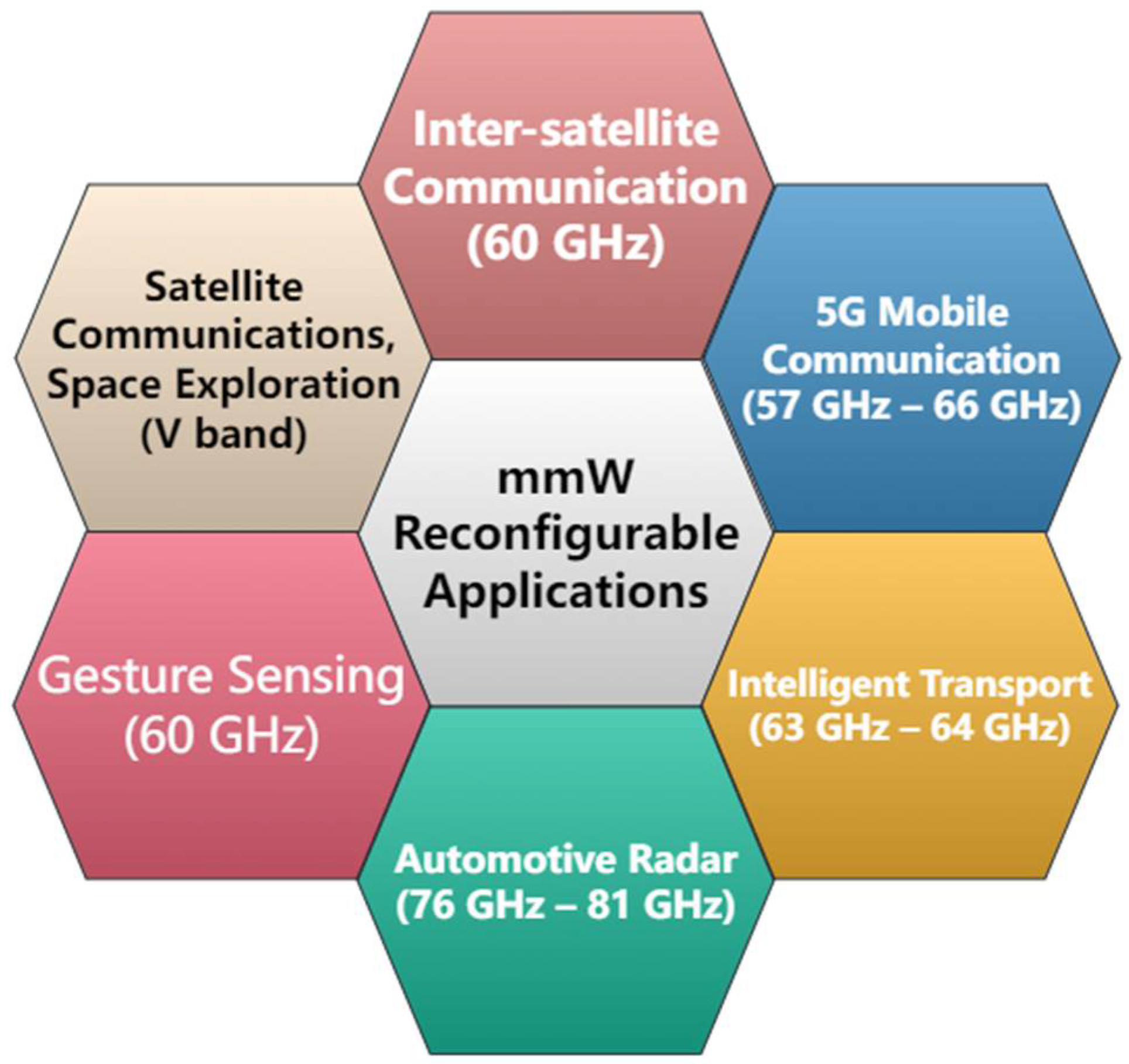
:1. Introduction
2. Materials and Methods
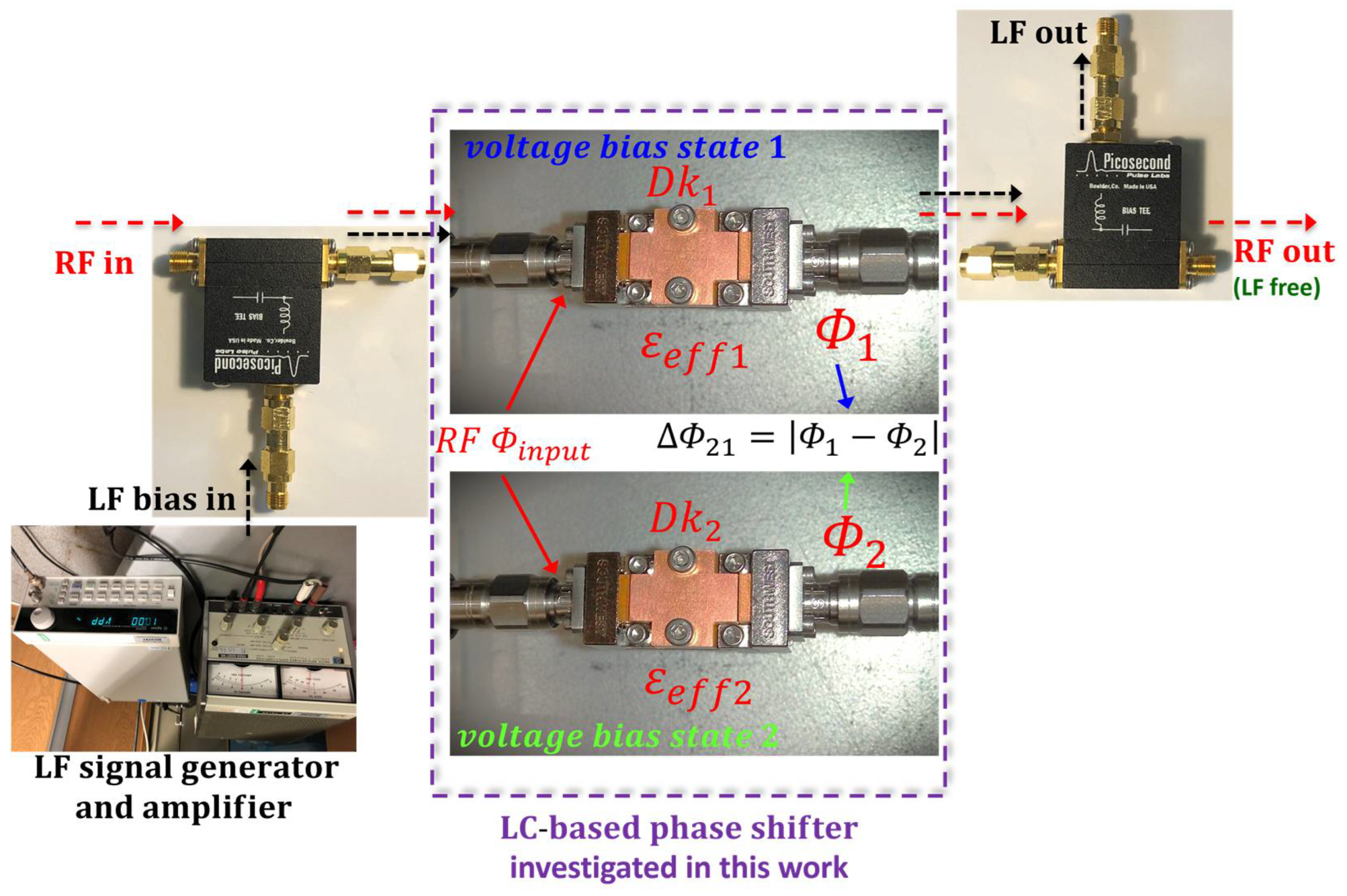
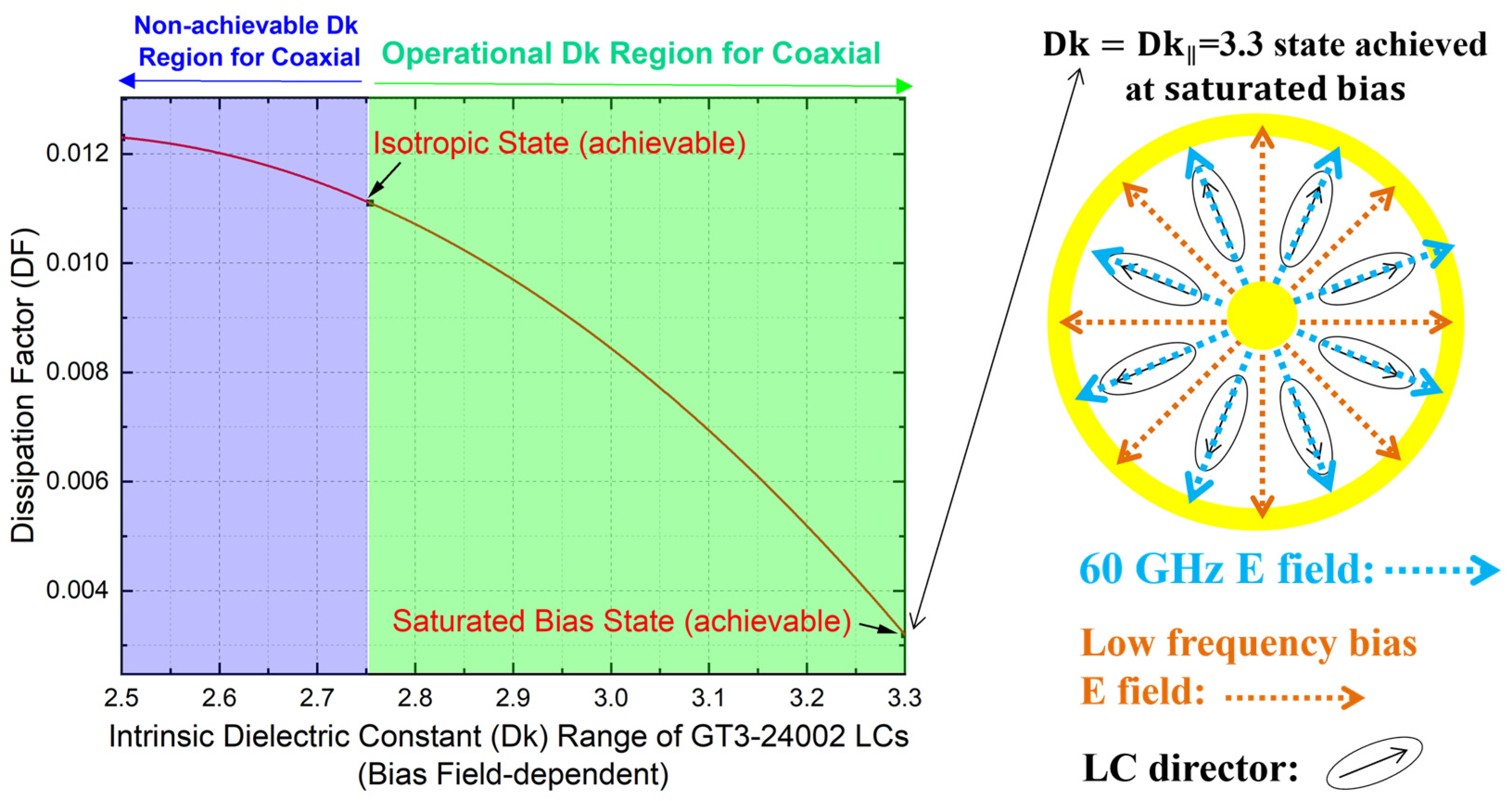
2.1. Tuning Mechanisms and Tuning States Investigations
2.2. mmW Power-Occupying Volume Ratio in Tunable Dielectrics
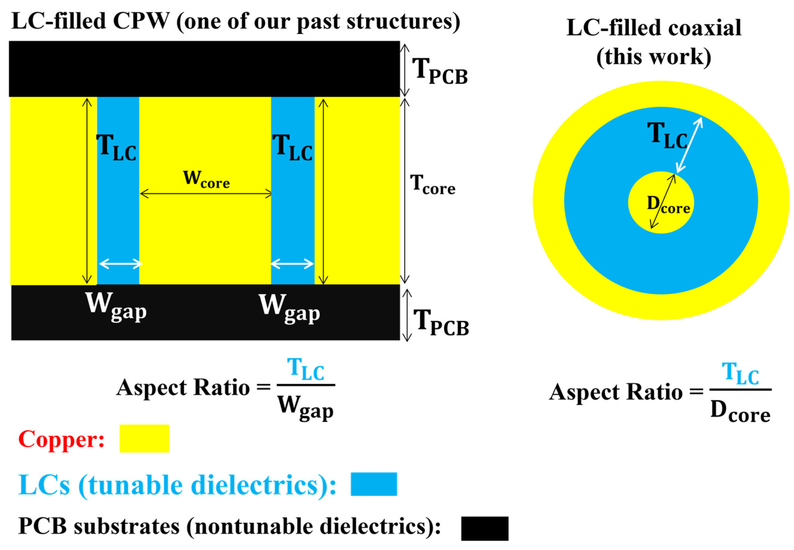
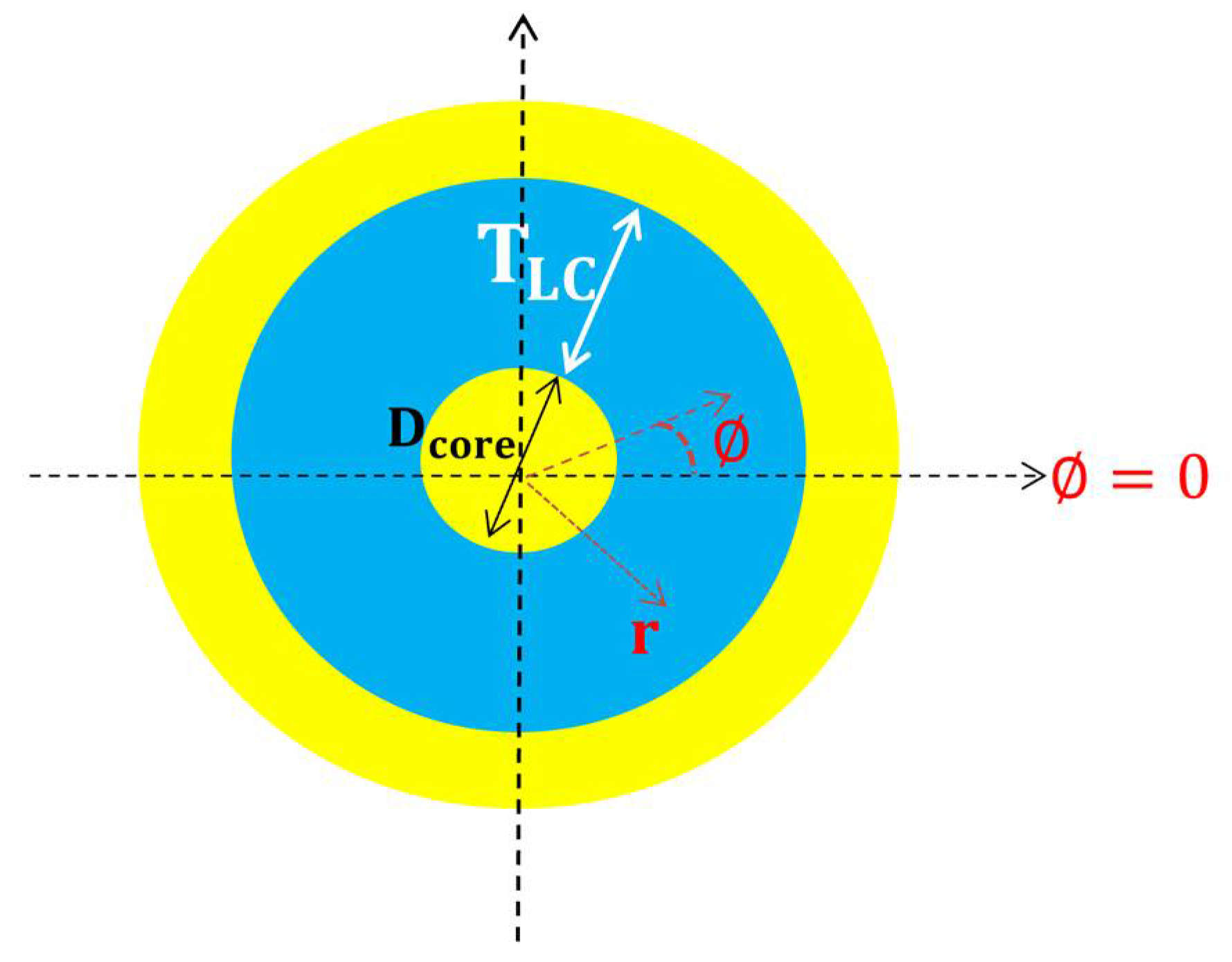
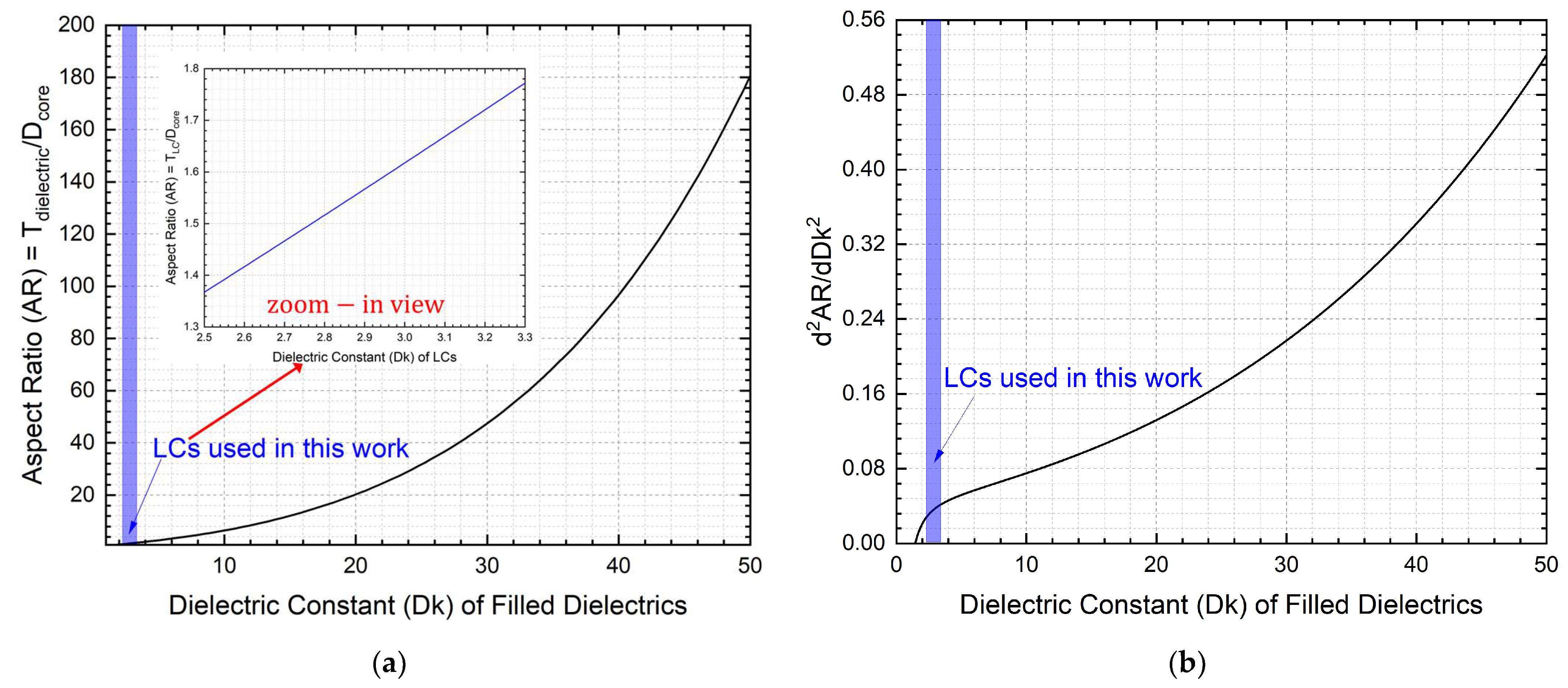
2.3. Cross-Sectional Geometry Investigations through the Lens of Aspect Ratio
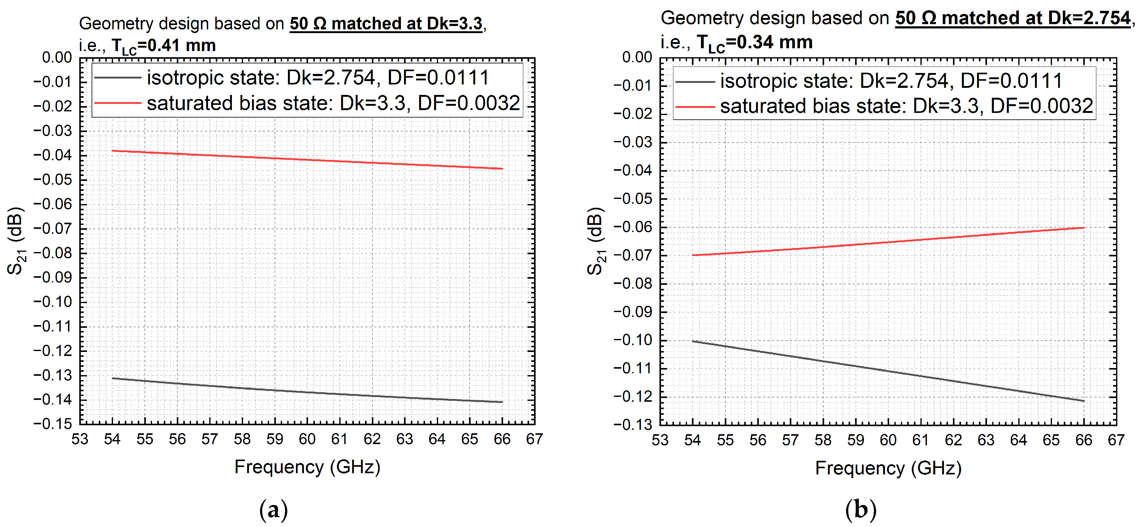
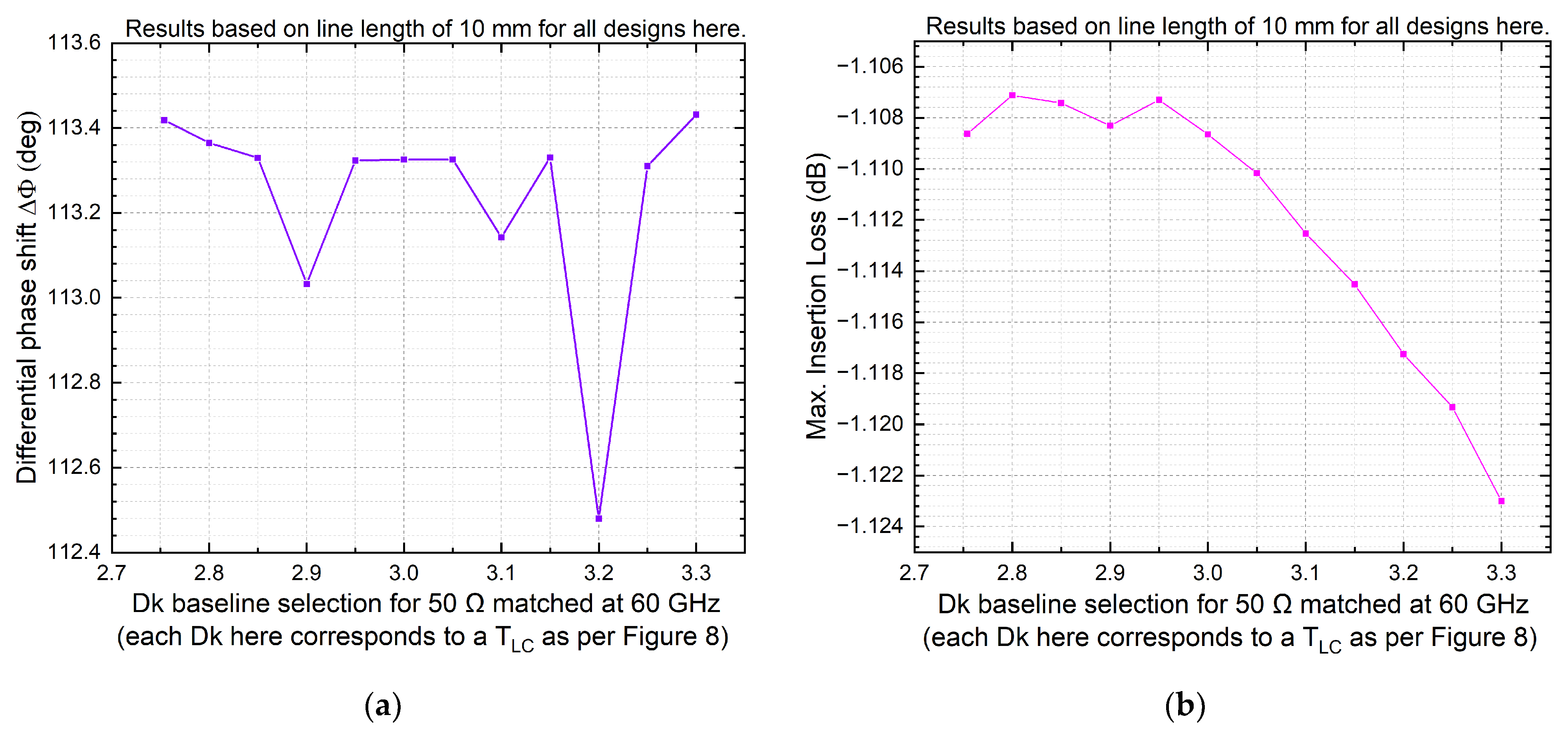
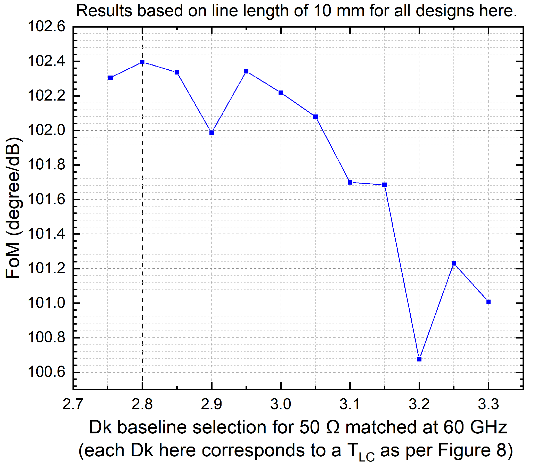
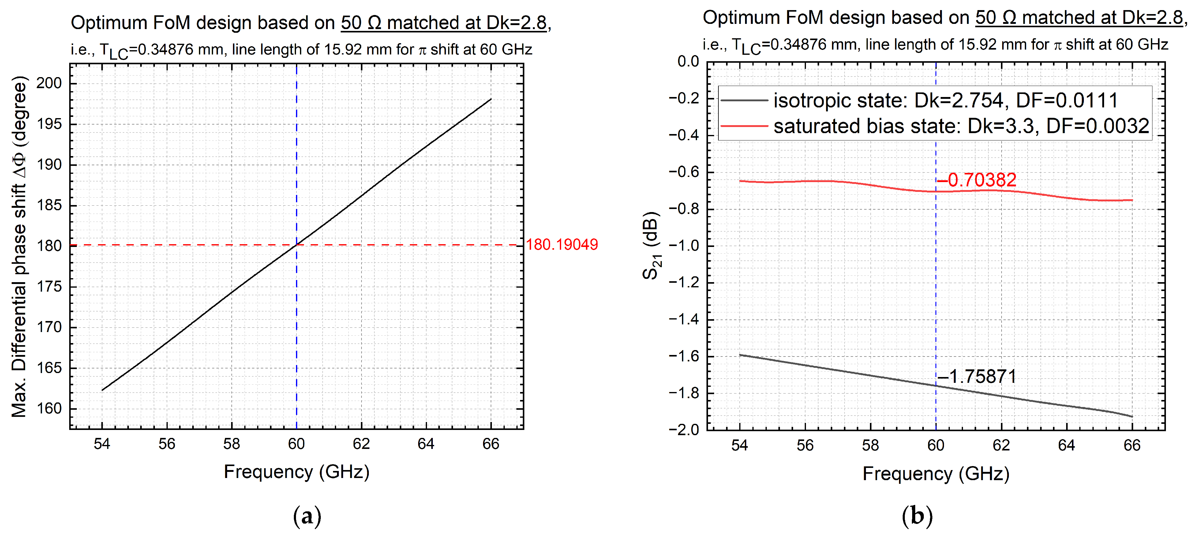
2.4. Novel Impedance Matching Baseline Method for FoM Enhancement
2.5. Loss Components Decomposition Analysis
2.6. Development Procedures and Protocols
3. Simulation Results and Discussions
3.1. Impedance Calculations and Aspect Ratio Effects
3.2. Effective Permittivity and mmW-PoVR Quantifications
3.3. Evaluation of Phase Shift and Insertion Loss Variations across Various Tuning States
3.4. Performance Comparison with Other States-of-the-Art Structures and Discussions
4. Concluding Remarks and Outlook
Author Contributions
Funding
Data Availability Statement
Conflicts of Interest
References
- Bonacchini, G.E.; Omenetto, F.G. Reconfigurable microwave metadevices based on organic electrochemical transistors. Nat. Electron. 2021, 4, 424–428. [Google Scholar] [CrossRef]
- Chan, K.Y.; Ramer, R. Millimeter-wave reconfigurable bandpass filters. Int. J. Microw. Wirel. Technol. 2015, 7, 671–678. [Google Scholar] [CrossRef]
- Burasa, P.; Mnasri, B.; Wu, K. Millimeter-Wave CMOS Sourceless Receiver Architecture for 5G-Served Ultra-Low-Power Sensing and Communication Systems. IEEE Trans. Microw. Theory Tech. 2019, 67, 1688–1696. [Google Scholar] [CrossRef]
- Topak, E.; Hasch, J.; Wagner, C.; Zwick, T. A Novel Millimeter-Wave Dual-Fed Phased Array for Beam Steering. IEEE Trans. Microw. Theory Tech. 2013, 61, 3140–3147. [Google Scholar] [CrossRef]
- Giuliano, R.; Mazzenga, F.; Vizzarri, A.; Vegni, A.M. Adaptable Communication System (ACS) for Flexible Communications in the Transport Sector: The AB4Rail project experience. In Proceedings of the 2021 AEIT International Conference on Electrical and Electronic Technologies for Automotive, Torino, Italy, 17–19 November 2021. [Google Scholar]
- Uddin, M.R.; Law, F.K.; Jalal, A.H. Design and simulation of an electro-optic even parity bit error detection system. Opt. Quant. Electron. 2021, 53, 593. [Google Scholar] [CrossRef]
- Basharat, S.; Khan, M.; Iqbal, M.; Hashmi, U.S.; Zaidi, S.A.R.; Robertson, I. Exploring reconfigurable intelligent surfaces for 6G: State-of-the-art and the road ahead. IET Commun. 2022, 16, 1458–1474. [Google Scholar] [CrossRef]
- Sanjari, P.; Aflatouni, F. An integrated photonic-assisted phased array transmitter for direct fiber to mm-wave links. Nat Commun. 2023, 14, 1414. [Google Scholar] [CrossRef] [PubMed]
- Trzebiatowski, K.; Rzymowski, M.; Kulas, L.; Nyka, K. Simple Millimeter Wave Identification System Based on 60 GHz Van Atta Arrays. Sensors 2022, 22, 9809. [Google Scholar] [CrossRef] [PubMed]
- Rzaik, N.; Dehos, C.; Zarudniev, M.; Siligaris, A.; Gonzalez, J.L.J. A mmW RadCom System for Short-Range Hand Gesture Sensing and Data Synchronization. In Proceedings of the 2023 18th Conference on Ph.D Research in Microelectronics and Electronics, Valencia, Spain, 18–21 June 2023. [Google Scholar]
- Li, J. Millimetre-wave beam steering with analog-resolution and minimised distortion based on liquid crystals tunable delay lines with enhanced signal-to-noise ratios. In Millimetre Wave and Terahertz Sensors and Technology XIII; SPIE: Bellingham, WA, USA, 2020; Volume 11541, pp. 68–73. [Google Scholar]
- Zaid, F.N.M.; Azemi, S.N.; Beson, M.R.C. Application of FSS for Microstrip Antenna for Gain Enhancement. IOP Conf. Ser. 2020, 767, 012001. [Google Scholar] [CrossRef]
- Hirabayashi, K.; Wada, M.; Amano, C. Liquid crystal variable optical attenuators integrated on planar lightwave circuits. IEEE Photonics Technol. Lett. 2001, 13, 609–611. [Google Scholar] [CrossRef]
- Arshad, F.; Ahmad, A.; Amin, Y.; Abbasi, M.A.B.; Choi, D.Y. MIMO antenna array with the capability of dual polarization reconfiguration for 5G mm-wave communication. Sci. Rep. 2022, 12, 18298. [Google Scholar] [CrossRef]
- Asfour, R.; Khamas, S.K.; Ball, E.A. Cost-Effective Design of Polarization and Bandwidth Reconfigurable Millimeter-Wave Loop Antenna. Sensors 2023, 23, 9628. [Google Scholar] [CrossRef]
- Qamar, Z.; Zheng, S.Y.; Chan, W.S.; Ho, D. An Equal-Length Multiway Differential Metamaterial Phase Shifter. IEEE Trans. Microw. Theory Tech. 2017, 65, 136–146. [Google Scholar] [CrossRef]
- Li, J. Rethinking Figure-of-Merits of Liquid Crystals Shielded Coplanar Waveguide Phase Shifters at 60 GHz. J 2021, 4, 444–451. [Google Scholar] [CrossRef]
- Abdulazhanov, S.; Le, Q.H.; Huynh, D.K.; Wang, D.; Gerlach, G.; Kämpf, T. A mmWave Phase Shifter Based on Ferroelectric Hafnium Zirconium Oxide Varactors. In Proceedings of the 2019 IEEE MTT-S International Microwave Workshop Series on Advanced Materials and Processes for RF and THz Applications, Bochum, Germany, 16–18 July 2019; pp. 175–177. [Google Scholar]
- Sohn, I.B.; Choi, H.K.; Noh, Y.C.; Kim, J.; Ahsan, M.S. Laser assisted fabrication of micro-lens array and characterization of their beam shaping property. Appl. Surf. Sci. 2019, 479, 375–385. [Google Scholar] [CrossRef]
- Uddin, M.R.; Wallner, J.; Dikshit, A.; Hossain, M.J.; Timalsina, Y.; Fahrenkopf, N.M.; Harame, D.L. Cascaded ring resonator based wide stop-band filter fabricated in AIM photonics technology at Albany Nanotech Complex. Proc. SPIE 2023, 12424, 124240U. [Google Scholar]
- Choi, H.K.; Jung, Y.J.; Yu, B.A.; Sung, J.H.; Sohn, I.B.; Kim, J.Y.; Ahsan, M.S. Femtosecond-Laser-Assisted Fabrication of Radiation-Resistant Fiber Bragg Grating Sensors. Appl. Sci. 2022, 12, 886. [Google Scholar] [CrossRef]
- Outram, B. Nematic liquid crystals. In Liquid Crystals, 1st ed.; IOP Publishing: Bristol, UK, 2018; Volume 4, pp. 1–14. [Google Scholar]
- Muller, S.; Scheele, P.; Weil, C.; Wittek, M.; Hock, C.; Jakoby, R. Tunable passive phase shifter for microwave applications using highly anisotropic liquid crystals. In Proceedings of the IEEE MTT-S International Microwave Symposium Digest, Fort Worth, TX, USA, 6–11 June 2004; pp. 1153–1156. [Google Scholar]
- Li, J.; Chu, D. Liquid Crystal-Based Enclosed Coplanar Waveguide Phase Shifter for 54–66 GHz Applications. Crystals 2019, 9, 650. [Google Scholar] [CrossRef]
- Mueller, S.; Goelden, F.; Scheele, P.; Wittek, M.; Hock, C.; Jakoby, R. Passive Phase Shifter for W-Band Applications using Liquid Crystals. In Proceedings of the 2006 European Microwave Conference, Manchester, UK, 10–15 September 2006; pp. 306–309. [Google Scholar]
- Reese, R.; Polat, E.; Tesmer, H.; Strobl, J.; Schuster, C.; Nickel, M.; Granja, A.B.; Jakoby, R.; Maune, H. Liquid Crystal Based Dielectric Waveguide Phase Shifters for Phased Arrays at W-Band. IEEE Access 2019, 7, 127032–127041. [Google Scholar] [CrossRef]
- Hähsler, M.; Nádasi, H.; Feneberg, M.; Marino, S.; Giesselmann, F.; Behrens, S.; Eremin, A. Magnetic Tilting in Nematic Liquid Crystals Driven by Self-Assembly. Adv. Funct. Mater. 2021, 31, 2101847. [Google Scholar] [CrossRef]
- Yazdanpanahi, M.; Syahkal, D.M. Millimeter-wave liquid-crystal-based tunable bandpass filter. In Proceedings of the 2012 IEEE Radio and Wireless Symposium, Santa Clara, CA, USA, 15–18 January 2012; pp. 139–142. [Google Scholar]
- Li, J. Rethinking Liquid Crystal Tunable Phase Shifter Design with Inverted Microstrip Lines at 1–67 GHz by Dissipative Loss Analysis. Electronics 2023, 12, 421. [Google Scholar] [CrossRef]
- Christou, M.A.; Papanicolaou, N.C.; Polycarpou, A.C. A nematic liquid crystal tunable patch antenna. In Proceedings of the 8th European Conference on Antennas and Propagation (EuCAP 2014), Hague, The Netherlands, 6–11 April 2014; pp. 1875–1878. [Google Scholar]
- Nobles, J.E.; Smiley, K.; Baques, D.B.; Economou, E.; Herman, J.; Harward, I.; Glushchenko, A.; Camley, R.E.; Celinski, Z. Eight-element liquid crystal based 32 GHz phased array antenna with improved time response. Eng. Res. Express 2021, 3, 045033. [Google Scholar] [CrossRef]
- Li, J. Novel Partially-Shielded Coplanar Waveguide with Metasurfaces for Liquid Crystals Tunable Delay Lines Beyond 67 GHz. In Proceedings of the 2022 IEEE Conference on Antenna Measurements & Applications (IEEE CAMA), Guangzhou, China, 14–17 December 2022; pp. 1–4. [Google Scholar]
- Li, J. 79 GHz Meandering Enclosed-Coplanar Variable Delay Lines in Liquid Crystals Encapsulated Within Independent and Shared Cavities. In Proceedings of the IEEE 27th International Symposium on Antennas and Propagation (ISAP), Sydney, Australia, 31 October–3 November 2022; pp. 457–458. [Google Scholar]
- Li, J. 60 GHz 0-360° Passive Analog Delay Line in Liquid Crystal Technology based on a Novel Conductor-backed Fully-enclosed Coplanar Waveguide. In Proceedings of the 2022 IEEE 72nd Electronic Components and Technology Conference (ECTC), San Diego, CA, USA, 31 May–3 June 2022; pp. 1841–1846. [Google Scholar]
- Heekwon, L.; Soojung, R.; Seungbae, L.; Kim, S.; Nah, W. Electromagnetic Field Interference on Transmission Lines due to On-Board Antenna. Int. J. Antennas Propag. 2015, 2015, 104506. [Google Scholar]
- Li, J. Will ‘Liquid-Crystal-Based Floating-Electrode-Free Coplanar Waveguide Phase Shifter with an Additional Liquid-Crystal Layer for 28-GHz Applications’ Work? ” Eng. Lett. 2023, 31, 820–824. [Google Scholar]
- Li, J.; Xu, H.; Chu, D. Design of liquid crystal based coplanar waveguide tunable phase shifter with no floating electrodes for 60–90 GHz applications. In Proceedings of the 2016 46th European Microwave Conference (EuMC), London, UK, 4–6 October 2016; pp. 1047–1050. [Google Scholar]
- Dhruvakumar, T.; Chaturvedi, A. Intelligent Reflecting Surface assisted millimeter wave communication for achievable rate and coverage enhancement. Veh. Commun. 2022, 33, 100431. [Google Scholar] [CrossRef]
- Jost, M.; Strunck, S.; Heunisch, A.; Wiens, A.; Prasetiadi, A.E.; Weickhmann, C.; Schulz, B.; Quibeldey, M.; Karabey, O.H.; Rabe, T.; et al. Continuously tuneable liquid crystal based stripline phase shifter realised in LTCC technology. In Proceedings of the 2015 European Microwave Conference (EuMC), Paris, France, 7–10 September 2015; pp. 1260–1263. [Google Scholar]
- Alloatti, L.; Pfeifle, J.; Mendez, J.; Freude, W.; Leuthold, J.; Koos, C. Liquid crystal phase shifter on the SOH platform with ultra-low power consumption. In Proceedings of the OFC/NFOEC, Los Angeles, CA, USA, 4–8 March 2012; pp. 1–3. [Google Scholar]
- Li, J. 60 GHz Optimised Nickel-free Gold-plated Enclosed Coplanar Waveguide Liquid Crystal Phase Shifter. In Proceedings of the 2020 IEEE MTT-S International Microwave Workshop Series on Advanced Materials and Processes for RF and THz Applications (IMWS-AMP), Suzhou, China, 29–31 July 2020; pp. 1–3. [Google Scholar]
- Li, J. Wideband PCB-to-Connectors Impedance Adapters for Liquid Crystal-Based Low-Loss Phase Shifters. In Proceedings of the 50th European Microwave Conference (EuMC), Utrecht, The Netherlands, 12–14 January 2021; pp. 546–549. [Google Scholar]
- Reese, R.; Polat, E.; Jost, M.; Nickel, M.; Jakoby, R.; Maune, H. Liquid crystal based phase shifter in a parallel-plate dielectric waveguide topology at V-band. In Proceedings of the 2017 12th European Microwave Integrated Circuits Conference (EuMIC), Nuremberg, Germany, 8–10 October 2017; pp. 353–356. [Google Scholar]
- Polat, E.; Reese, R.; Jost, M.; Nickel, M.; Schuster, C.; Jakoby, R.; Maune, H. Liquid Crystal Phase Shifter Based on Nonradiative Dielectric Waveguide Topology at W-Band. In Proceedings of the 2019 IEEE MTT-S International Microwave Symposium (IMS), Boston, MA, USA, 2–7 June 2019; pp. 184–187. [Google Scholar]
- Reese, R.; Jost, M.; Maune, H.; Jakoby, R. Design of a continuously tunable W-band phase shifter in dielectric waveguide topology. In Proceedings of the 2017 IEEE MTT-S International Microwave Symposium (IMS), Honololu, HI, USA, 4–9 June 2017; pp. 180–183. [Google Scholar]
- Hu, W.; Jiang, D.; Zhang, W.; Liu, Y.; Zhu, K.; Zhang, T. Design of a W-Band Dielectric Phase Shifter Based on Liquid Crystal. Int. J. Antennas Propag. 2022, 2022, 6486628. [Google Scholar]
- Jost, M.; Weickhmann, C.; Strunck, S.; Gäbler, A.; Fritzsch, C.; Karabey, O.H.; Jakoby, R. Liquid crystal based low-loss phase shifter for W-band frequencies. Electron. Lett. 2013, 49, 1460–1462. [Google Scholar] [CrossRef]
- Nova, V.; Bachiller, C.; Villacampa, B.; Kronberger, R.; Boria, V.E. Characterization of Nematic Liquid Crystals at Microwave Frequencies. Crystals 2020, 10, 1106. [Google Scholar] [CrossRef]
- Christie, S.; Cahill, R.; Mitchell, N.; Munro, Y.; Manabe, A. Electronically scanned Rotman lens antenna with liquid crystal phase shifters. Electron. Lett. 2013, 49, 445–447. [Google Scholar] [CrossRef]
- Cai, L.; Chu, D. Compact liquid crystal based phase shifter with integrated bias tees. In Proceedings of the 2018 IEEE MTT-S International Wireless Symposium (IWS), Chengdu, China, 6–10 May 2018; pp. 1–4. [Google Scholar]
- Prasetiadi, A.E.; Karabey, O.H.; Weickhmann, C.; Franke, T.; Hu, W.; Jost, M.; Nickel, M.; Jakoby, R. Continuously tunable substrate integrated waveguide bandpass filter in liquid crystal technology with magnetic biasing. Electron. Lett. 2015, 51, 1584–1585. [Google Scholar] [CrossRef]
- Li, X.; Sato, H.; Shibata, Y.; Ishinabe, T.; Fujikake, H.; Chen, Q. Development of Beam Steerable Reflectarray with Liquid Crystal for Both E-Plane and H-Plane. IEEE Access 2022, 10, 26177–26185. [Google Scholar] [CrossRef]
- Polat, E.; Tesmer, H.; Reese, R.; Nickel, M.; Wang, D.; Schumacher, P.; Jakoby, R.; Maune, H. Reconfigurable Millimeter-Wave Components Based on Liquid Crystal Technology for Smart Applications. Crystals 2020, 10, 346. [Google Scholar] [CrossRef]
- Wang, Q.; Su, Z.; Li, S.; Zhao, H.; Yin, X. Electrically tunable liquid crystal phase shifter with excellent phase shift capability per wavelength based on opposed coplanar waveguide. J. Phys. D Appl. Phys. 2022, 55, 405001. [Google Scholar] [CrossRef]
- Polat, E.; Kamrath, F.; Matic, S.; Tesmer, H.; Jiménez-Sáez, A.; Wang, D.; Maune, H.; Höft, M.; Jakoby, R. Novel Hybrid Electric/Magnetic Bias Concept for Tunable Liquid Crystal Based Filter. IEEE J. Microw. 2022, 2, 490–495. [Google Scholar] [CrossRef]
- Nickel, M.; Jiménez-Sáez, A.; Agrawal, P.; Gadallah, A.; Malignaggi, A.; Schuster, C.; Reese, R.; Tesmer, H.; Polat, E.; Wang, D.; et al. Ridge Gap Waveguide Based Liquid Crystal Phase Shifter. IEEE Access 2020, 8, 77833–77842. [Google Scholar] [CrossRef]
- Kinoshita, Y.; Uchida, N. Flow patterns and defect dynamics of active nematic liquid crystals under an electric field. Phys. Rev. E 2023, 108, 014605. [Google Scholar] [CrossRef] [PubMed]
- Hieber, M.; Nesensohn, M.; Prüss, J.; Schade, K. Dynamics of nematic liquid crystal flows: The quasilinear approach. Ann. Inst. Henri Poincare (C) Anal. Non Lineaire 2016, 33, 397–408. [Google Scholar] [CrossRef]
- Attila, A. Stability of nematic liquid crystals under a temperature gradient. Calculations for PAA. Int. J. Eng. Sci. 1976, 14, 259–271. [Google Scholar]
- Bouriche, A.; Alachaher-Bedjaoui, L.; Barrera, A.; Staelens, J.N.; Maschke, U. Thermal Degradation Studies of Poly(2-ethyl hexyl acrylate) in the Presence of Nematic Liquid Crystals. Polymers 2023, 15, 3934. [Google Scholar] [CrossRef] [PubMed]
- Woehrle, C.D.; Doyle, D.T.; Lane, S.A.; Christodoulou, C.G. Space Radiation Environment Testing of Liquid Crystal Phase Shifter Devices. IEEE Antennas Wirel. Propag. Lett. 2015, 15, 1923–1926. [Google Scholar] [CrossRef]
- Gaebler, A.; Moessinger, A.; Goelden, F.; Manabe, A.; Goebel, M.; Follmann, R.; Koether, D.; Modes, C.; Kipka, A.; Deckelmann, M.; et al. Liquid Crystal-Reconfigurable Antenna Concepts for Space Applications at Microwave and Millimeter Waves. Int. J. Antennas Propag. 2009, 2009, 876989. [Google Scholar] [CrossRef]
- Nestoros, M.; Papanicolaou, N.C.; Polycarpou, A.C. Design of beam-steerable array for 5G applications using tunable liquid crystal phase shifters. In Proceedings of the 2019 13th European Conference on Antennas and Propagation (EuCAP), Krakow, Poland, 31 March–5 April 2019; pp. 1–4. [Google Scholar]
- Jakoby, R.; Gaebler, A.; Weickhmann, C. Microwave liquid crystal enabling technology for electronically steerable antennas in SATCOM and 5G millimeter-wave systems. Crystals 2020, 10, 514. [Google Scholar] [CrossRef]
- Camacho-Gomez, C.; Sanchez-Montero, R.; Martínez-Villanueva, D.; López-Espí, P.L.; Salcedo-Sanz, S. Design of a Multi-Band Microstrip Textile Patch Antenna for LTE and 5G Services with the CRO-SL Ensemble. Appl. Sci. 2020, 10, 1168. [Google Scholar] [CrossRef]
- Doré, J.B.; Belot, D.; Mercier, E.; Bicaïs, S.; Gougeon, G.; Corre, Y.; Miscopein, B.; Kténas, D.; Strinati, E.C. Technology Roadmap for Beyond 5G Wireless Connectivity in D-band. In Proceedings of the 2020 2nd 6G Wireless Summit (6G SUMMIT), Levi, Finland, 17–20 March 2020; pp. 1–5. [Google Scholar]
- Wang, C.X.; You, X.; Gao, X.; Zhu, X.; Li, Z.; Zhang, C.; Wang, H.; Huang, Y.; Chen, Y.; Haas, H.; et al. On the Road to 6G: Visions, Requirements, Key Technologies, and Testbeds. IEEE Commun. Surv. Tutor. 2023, 25, 905–974. [Google Scholar] [CrossRef]
- Mourad, A.; Yang, R.; Lehne, P.H.; De La Oliva, A. A Baseline Roadmap for Advanced Wireless Research Beyond 5G. Electronics 2020, 9, 351. [Google Scholar] [CrossRef]
- Dangi, R.; Choudhary, G.; Dragoni, N.; Lalwani, P.; Khare, U.; Kundu, S. 6G Mobile Networks: Key Technologies, Directions, and Advances. Telecom 2023, 4, 836–876. [Google Scholar] [CrossRef]
- Jiang, W.; Han, B.; Habibi, M.A.; Schotten, H.D. The Road Towards 6G: A Comprehensive Survey. IEEE Open J. Commun. Soc. 2021, 2, 334–366. [Google Scholar] [CrossRef]
- Bhat, J.R.; Alqahtani, S.A. 6G Ecosystem: Current Status and Future Perspective. IEEE Access 2021, 9, 43134–43167. [Google Scholar] [CrossRef]
- De Alwis, C.; Kalla, A.; Pham, Q.V.; Kumar, P.; Dev, K.; Hwang, W.J.; Liyanage, M. Survey on 6G Frontiers: Trends, Applications, Requirements, Technologies and Future Research. IEEE Open J. Commun. Soc. 2021, 2, 836–886. [Google Scholar] [CrossRef]
- Penttinen, J.T.J. On 6G Visions and Requirements. J. ICT Stand. 2021, 9, 311–325. [Google Scholar] [CrossRef]
- Kumar, R.; Gupta, S.K.; Wang, H.C.; Kumari, C.S.; Korlam, S.S.V.P. From Efficiency to Sustainability: Exploring the Potential of 6G for a Greener Future. Sustainability 2023, 15, 16387. [Google Scholar] [CrossRef]


| Structures | FoM (°/dB) | Line Length (mm) | Workable Range of Dk | PI Requirement (Baking, Rubbing) | CTE * Mismatch Problem |
|---|---|---|---|---|---|
| Inverted microstrip model [29] | 112.17 | 13.50 | 2.5–3.3 | Required | Significant |
| Enclosed coplanar model [24] | 109.09 | 14.32 | 2.5–3.3 | Required | Significant |
| Enclosed coplanar measured [24] | 40.79 | 15.75 | 2.5–3.3 | Required | Significant |
| Coaxial model (this work) | 102.46 | 15.92 | 2.754–3.3 | Not required | Minimized |
Disclaimer/Publisher’s Note: The statements, opinions and data contained in all publications are solely those of the individual author(s) and contributor(s) and not of MDPI and/or the editor(s). MDPI and/or the editor(s) disclaim responsibility for any injury to people or property resulting from any ideas, methods, instructions or products referred to in the content. |
© 2024 by the authors. Licensee MDPI, Basel, Switzerland. This article is an open access article distributed under the terms and conditions of the Creative Commons Attribution (CC BY) license (https://creativecommons.org/licenses/by/4.0/).
Share and Cite
Li, J.; Li, H. Liquid Crystal-Filled 60 GHz Coaxially Structured Phase Shifter Design and Simulation with Enhanced Figure of Merit by Novel Permittivity-Dependent Impedance Matching. Electronics 2024, 13, 626. https://doi.org/10.3390/electronics13030626
Li J, Li H. Liquid Crystal-Filled 60 GHz Coaxially Structured Phase Shifter Design and Simulation with Enhanced Figure of Merit by Novel Permittivity-Dependent Impedance Matching. Electronics. 2024; 13(3):626. https://doi.org/10.3390/electronics13030626
Chicago/Turabian StyleLi, Jinfeng, and Haorong Li. 2024. "Liquid Crystal-Filled 60 GHz Coaxially Structured Phase Shifter Design and Simulation with Enhanced Figure of Merit by Novel Permittivity-Dependent Impedance Matching" Electronics 13, no. 3: 626. https://doi.org/10.3390/electronics13030626