Abstract
The advantage of FPGAs lies in their ability to implement a fully hardware solution for interfacing with various input/output (I/O) devices. Each block can work in parallel with all the others, simplifying the satisfaction of timing constraints. However, this hardware utilization consumes FPGA resources that could otherwise be allocated to the primary project. An alternative involves employing a small “soft-core” processor to implement I/O in software. With the goal of designing and evaluating a new tiny soft-core processor optimized for FPGA resources in I/O, a novel processor named Baby8 is developed. It is an 8-bit CISC soft-core processor optimized for reduced FPGA resources, including program size for 8-bit applications. The number of instructions is not large, but any instruction can access arbitrary memory locations. The performance and resource utilization of the newly designed processor are evaluated and compared with a variety of other soft-core processors. The results demonstrate its competitive performance, achieving an average maximum clock frequency of approximately 57 MHz and a power consumption of around 2 mW. Furthermore, it conserves nearly half of the FPGA resources in implementation.
1. Introduction
FPGAs offer the flexibility to implement a fully operational hardware solution for interfacing with diverse I/O devices, allowing the blocks to operate in parallel, simplifying their timing constraint fulfillment. However, the drawback is the consumption of FPGA resources that could be directed towards the main project. A viable alternative is employing a small “soft-core” processor for software-based I/O implementation. This approach saves resources in two ways: block RAM bits are smaller compared to separate flip-flops in configurable blocks, and a processor can time multiplex operations like adders, unlike the hardware solution with multiple unused copies. The performance only needs to be sufficient for protocol implementation, making the trade-off between fewer resources and speed. To achieve this goal, a new processor called Baby8, designed for FPGA I/O, is being developed using Yosys Synthesis software version 0.38 [1,2].
Baby8 is a von Neumann 8-bit CISC soft-core processor (already available in the authors’ GitHub repository in [3]) optimized for reduced FPGA resources, including program size for 8-bit applications. Although the instruction set is not extensive, each instruction can access an arbitrary memory location. Features like post-increment addressing, while not faster than RISC (instructions use simple register-level [4]), enhance program compactness and may reduce the need for block RAMs. This paper presents a comparison of Baby8 with almost a dozen other soft-core processors, demonstrating competitive performance in terms of implementation results, and comparisons with ASIC, NAND gates, and various FPGA models.
1.1. ASICs
Application-specific integrated circuits are those designed to be used in one particular product, as opposed to standard integrated circuits that are sold to many companies to be used in many products. While the cost of each ASIC is normally a fraction of the cost of an FPGA capable of handling the same design, the production of the ASIC has some high NRE (non-recurring engineering) costs, so a reasonably high volume is needed for the ASIC to be more viable economically than a FPGA. Additionally, ASICs may operate at higher frequencies and lower power than FPGAs, impacting product considerations. Comparing processor cores involves assessing area, operating frequency, and power usage for a given fabrication technology.
1.2. NAND Gates
It is possible to build any digital circuit entirely with NAND logic gates or with just NOR gates (the case for the AGC, the Apollo Guidance Computer, which landed on the Moon). Before field-programmable gate arrays (FPGAs), many projects used gate arrays. These were chips that had a large number of NAND gates, the same for all clients, and the metal layer was specific to each client. Translating designs to NAND gates provides insights into design complexity using the OnlyNANDYosysSynth complement script to Yosys Synthesis software version 0.38.
1.3. FPGAs
Field-programmable gate arrays can implement any digital circuit up to a size that depends on the particular FPGA device. Using hardware description languages like Verilog, VHDL, Chisel, SpinalHDL, and others, a high-level processor description can be translated into a netlist of basic blocks. The placement tool assigns blocks to specific locations, and routing utilizes the FPGA’s configurable connection network. Routing uses the configurable connection network in the FPGA (a little like early telephone exchange systems) to actually connect the placed blocks. This is encoded into a “bit file” that is loaded by the FPGA each time it is turned on to actually implement the circuit.
This comparison considers the usage of basic blocks (LUT, registers, DSP, distributed memory, and block memory) in soft cores when translated with the open-source tool Yosys002E. The basic blocks are:
- LUT: LookUp tables implement all logic in FPGAs and can be categorized by the number of address lines they require. A LUT4 has 16 words of a single bit each and needs 4-bit addresses. A LUT6 has 64 bits and needs six address lines. A larger LUT can always perform the job of a smaller one by either tying unused address lines to zero or one or else duplicating the bits such that the output does not depend on that address line. Combining smaller LUTs into a larger one is facilitated by special “mux” blocks in some FPGAs (XC4000), enhancing their efficiency.
- Registers: The LUTs are purely combinational, and an optional flip–flop circuit at the output enables the implementation of sequential circuits. Normally, one register is associated with one LUT, but there tend to be some extra registers as part of the I/O pads.
- DSP: Digital signal processing blocks are hardware implementations of multiplication circuits. Otherwise, a very large number of LUTs would be required to implement this operation, which has many more uses beyond digital signal processing.
- Distributed memory: Each LUT is actually a very small random access memory (RAM), generally unaltered after the initial FPGA configuration. An additional circuit allows the use of all LUTs or a fraction as read/write memories.
- Block memory: The area needed to store a bit in a register or even in a LUT is very large compared to a dedicated RAM circuit. Since the 1990s, FPGAs have included a number of memory blocks that can efficiently handle a medium to large number of bits.
Other FPGA blocks include input and output buffers, clock buffers, and carry circuits converting LUTs into adder circuits, along with multiplexers for combining small LUTs and FPGA-specific circuits unique to each type.
FPGA Families
Xilinx 7: The 28 nm generation of Xilinx FPGAs remains popular, even after AMD’s acquisition and the introduction of two subsequent generations. It is common for soft-core processor implementation projects to make use of the FPGAs manufactured by Xilinx [5]. Cyclone V: The Cyclone family was the low end of Altera FPGAs, with the V generation being the last before Intel’s acquisition of Altera. ICE40: The startup Silicon Blue took advantage of the expiration of key FPGA patents to introduce their own very basic offering. Their focus was on smaller FPGAs with low costs and low energy requirements. They were bought by Lattice Semiconductor, and a second generation was designed, moving from the original 65nm process to a more modern 40nm process, further reducing the energy use. GoWin: This Chinese company achieved success with various FPGA variations globally, introducing unique features like using spare LUTs to aid routing. How much this is used varies from one project to the next, and this is why the numbers are not always relatively the same compared to other types of FPGAs. ECP5: An evolution of the earlier ECP, ECP2, and ECP3 FPGAs, the ECP5 family is a cost-effective mid-range option with high-speed serial interfaces.
1.4. RISC-V Soft Cores
The rising popularity of RISC-V [6] in the industrial and academic space resulted in a plethora of open-source RISC-V implementations [7,8]. The openness of the standard does not guarantee the openness of specific cores, but those considered in this paper are open. In addition, only cores implemented in Verilog or the subset of System Verilog handled by Yosys were considered. RISC-V cores have a tremendous range in performance and complexity [9], from tiny 32-bit microcontrollers to out-of-order 64-bit application cores for data centers. Only the low end was studied here. darkRISC-V: The original darkRISC-V was created by Samsoniuk in a single night of development to evaluate the advantages and disadvantages of the RISC-V instruction set compared to others. It can be optionally made smaller by reducing the number of registers as per RV32E. vexRISC-V: The vexRISC-V in SpinalHDL is meant to show off the advantages of using that language, with many configuration options where it is even easy to change the number of pipeline stages. Many projects use the translated Verilog version of the processor, like the management system in the repository for the GlobalFoundries 180 nm version of the Caravel “harness” for open-source ASIC design. Glacial: Glacial trades off performance for size by being an 8-bit processor that emulates a 32-bit RISC-V. One inspiration was the low end of the original IBM S/360 family, which used microcode and an 8-bit datapath to implement the architecture. PicoRV32: An early compact RISC-V core, the goal of the PicoRV32 was to fit in the tiny ICE40 FPGAs first targeted by the ICE Storm open-source FPGA tool, of which Yosys was a key component. SERV: SErial Risc V also trades off performance for size, in this case by having a completely serial implementation. This means that any operation requires 32 clock cycles, as the operation handles only a single bit in each cycle. Serial computers were a little more common in the days of vacuum tubes, when every single component had a significant cost and added to the construction cost as well. They became far rarer in the integrated circuit days, but they are one way to save FPGA resources best left for other parts of a project.
1.5. Other Soft Cores
Even with all the variation possible with the RISC-V instruction set, there are applications where other designs are a better option. That is particularly true when executing programs. Baby8: Designed to help interfaces adapt FPGA projects to specific boards, the goal of Baby8 is to use as few FPGA resources as possible to leave more for the user’s actual project (available in the authors’ GitHub repository in [3]). An 8-bit architecture is a good match for the applications of interfacing to PS/2 or USB keyboards, mice, and game controllers, as well as providing an abstract interface to files on a FAT32-formatted SD memory card. In a FPGA, distributed memory built from LUTs is denser than individual flip-flops. Baby8 capitalizes on this density, albeit at the cost of reduced performance, by incorporating the program counter into the register bank. In an ASIC, there is no advantage in doing this, as the flip-flops would be the same either way. The nomenclature of the processor was chosen in honor of the Manchester Baby, a 32-bit small-scale experimental machine and the first electronic stored-program computer in 1948 [10]. A complete description of the features and particularities of the Baby8 processor will be presented in the Materials and Methods Section of this paper. 6502 and UKP: A NES (Famicom) emulator for the Sipeed Tang Nano 20K FPGA board includes two processors. The 6502 is needed to run the actual games, while the limited UKP handles USB mice, keyboards, or game controllers. Femto16: In the 8-Bit Workshop online video game development system, there is an option to design games at the hardware level using Verilog. The examples grow in complexity, introducing two simple processors, the 8-bit Femto8 and the 16-bit Femto16. Games are then converted from pure hardware to assembly programs for these processors. J0: Describing the J1 soft core optimized for small programs in the Forth language was the inspiration for projects like SwapForth by the same author and the Forth CPU computer system. The Gameduino project adds FPGA-based video output for Arduino boards, incorporating the J0 processor as a slight modification of the J1. MCPU: With only four instructions and addressing only 64 bytes of memory (similar to Xilinx PicoBlaze), the MCPU is remarkably small yet Turing complete. ZPU: The ‘ZPU Avalanche’ was designed to use the least FPGA possible while being fully compatible with all the GNU programming tools, including GCC. The concept revolves around treating C as more of a scripting language on an FPGA, with heavy processing handled by hardware blocks. The Avalanche project translated the original VHDL implementation to System Verilog. The System Verilog files were copied from the original repository in the top directory.
2. Objectives
The main goal of our study is to design and evaluate a brand new soft-core processor optimized for reduced FPGA resources, including program size for 8-bit applications.
3. Materials and Methods
3.1. Processor Specifications
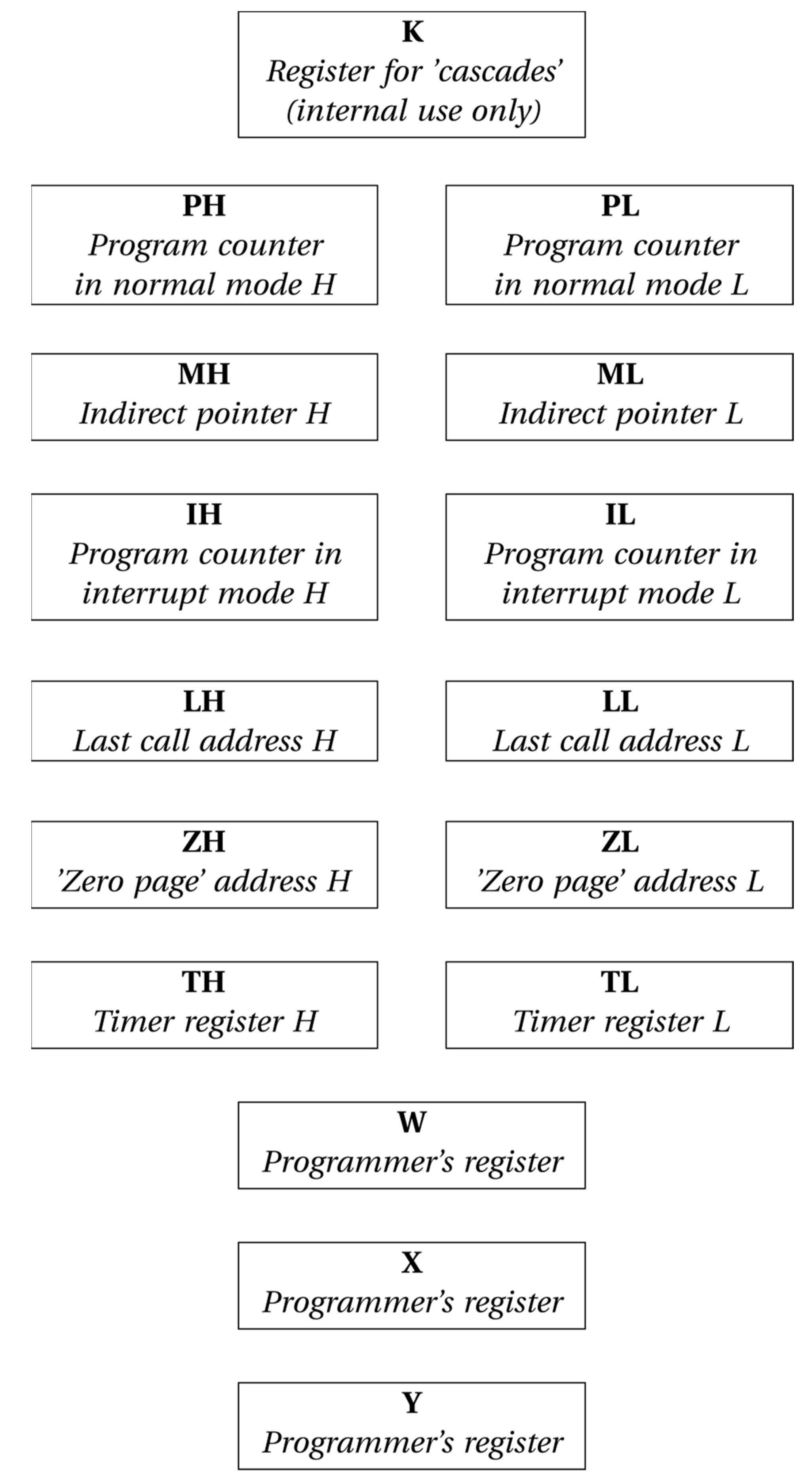
3.1.1. State Registers
The processor features 16 internal 8-bit state registers, as shown in Figure 1. While not accessible to programmers, exceptions include the registers W, X, and Y and the external memory, which can be directly read and written by the user program. Flags Z (zero), N (negative), C (carry), and V (overflow) do not persist between instructions but can be saved with TEST instructions.
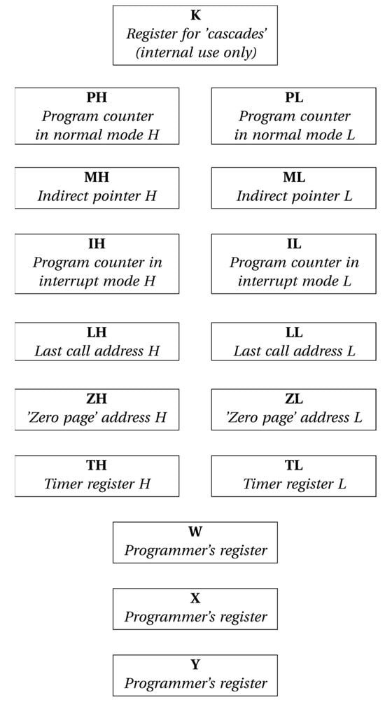
Figure 1.
The Baby8 processor’s 8-bit state registers. High- and low-forming 16-bit addresses.
The complete list of 8-bit state registers is provided in the following, where H denotes a high byte and L denotes a low byte in the case of 16-bit addressing:
- PH/PL: 16-bit (8H/8L) program counter in normal execution mode;
- MH/ML: 16-bit (8H/8L) pointer for indirect “zero page” operands;
- IH/IL: 16-bit (8H/8L) program counter in interrupt mode;
- LH/LL: 16-bit (8H/8L) address saved in the last call instruction;
- ZH/ZL: 16-bit (8H/8L) address of the “zero page” operand;
- TH/TL: 16-bit (8H/8L) timer to define the number of cycles to pause before the next instruction;
- K: 8-bit single register for ’cascades’—values between pairs of instructions;
- W, X, and Y: 8-bit single registers accessible to the programmers for reading and writing.
3.1.2. Basic Syntax
The processor was designed with a two-address architecture, where one address indicates both the destination and one operand, and the second address specifies the other operand. The assembly language syntax is C-like, with an addition represented as:
rD + = rS
3.1.3. K-Cascades
The “cascade” feature changes the destination to be the first operand of the following instruction. A sequence that is incremented by ‘the value pointed to by location 20’ looks like:
X + = *20
W & = X
It can be implemented with the cascade as:
K = X + *20
Y = W & K
Unlike the original code fragment, these two instructions do not erase the value in X. While the architecture is generally two-address, it can function as three addresses (actually four) when needed. The use of “K” in the instruction distinguishes it from a move with some complicated expression to be calculated at assembly time.
3.1.4. Source and Destination
Table 1 shows the source and destination directives in the processor architecture. In theory, the zero page allows access to bytes 0 to 127 of the 256-byte page selected by register ZH. In practice, addresses 12 to 15 access the four input and four output ports. More I/O ports can be memory-mapped to other addresses if needed.

Table 1.
Source and destination directives in Baby8 architecture.
Zero page addresses 0 to 11 access the internal registers W to IH, allowing LL and LH to be saved and restored if more than one level of subroutines is needed. Since ZH can also be changed, the “zero page” can be relocated to any memory location, similar to the 6809 and 65,816 processors. When TL is changed, the timer is started if TL and TH are not both zero, and it is stopped if they are zero.
The two-bit ss and dd fields (see Table 2) in the instruction use values 0, 1, and 2 to encode the registers W, X, and Y, respectively. A value of 3 indicates that a byte follows, encoding the actual address.
Table 2.
Regular and K-cascade basic instructions in Baby8.
When both ss and dd are 3, the first extra byte is for the source, and the second is for the other source/destination. In the case of immediate instructions, the immediate value is the first extra byte, followed by the destination.
Table 3.
Immediate instructions in Baby8.
Table 4.
Control flow instructions in Baby8.
Table 5.
Conditional tests in Baby8.
- The basic operations opcodes;
- The immediate instructions opcodes;
- The control flow instructions opcodes;
- The conditional tests.
3.1.5. Shifts and Rotations
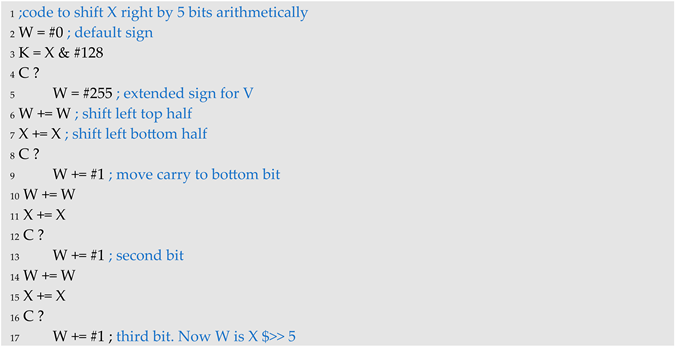
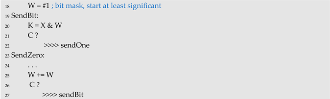
The missing multiplication and division instructions are to be expected for a very small processor (though they can be added as an I/O device if needed), but the lack of shift and rotate instructions might seem limiting. Adding a value to itself is equivalent to a one-bit shift to the left, with the carry indicating the removed bit. Shifting to the right (logical or arithmetic) an 8-bit value by N bits can be achieved by extending (zero or sign) to 16-bits, shifting that to the left by 8-N bits, and using the top byte as the result (Listing 1). Sending a byte with the least significant bit first might seem to require 7 such steps per bit, but the same result can be achieved by shifting a one-bit mask to the left once per step to check each bit from least to most significant (Listing 2).
| Listing 1. Shifts and rotations syntax example in Baby8. |
 |
| Listing 2. Shifts and rotations syntax example in Baby8. |
 |
3.1.6. Interrupt
The interrupt mode uses IH/IL for instruction fetches instead of PH,PL (bit 2 of the register addresses is 1), and zero page addresses go from 144 to 255 instead of from 16 to 127 (bit 7 of addresses is set). The interrupt mode is entered on the next instruction fetch after the interrupt line goes high, unless the previous instruction was a cascade or the current instruction is supposed to be skipped. The interrupt mode ends on the next instruction fetch after the interrupt line goes low, with the same restrictions as described before.
Most processors have interrupt handlers that start at fixed addresses or, more often, as indicated in some tables. In Baby8, the address in IH/IL is simply the instruction following the one that caused the interrupt line to go low at the end of the previous interrupt. This is more like a coroutine scheme where an explicit “yield” instruction is executed. With careful programming, it is possible to speed up response time by having the processor ready to execute in different places for different situations. Any registers used by the interrupt handler should be saved and then restored right before the yield. Having the use of the second half of the zero page makes this easier. Note that the first half can still be accessed with indirect addressing.
3.1.7. Timer
Every instruction is executed in a known number of clock cycles, but to make precise delays even easier, TH/TL implements a 16-bit timer. The timer mode is entered on the next instruction fetch after a write to TL, which results in TH or TL having a non-zero value. The restrictions are the same as entering or leaving interrupt mode.
Instead of fetching instructions, the processor simply decrements TL by one on every clock cycle. When TH/TL reaches zero, the instruction fetch resumes. If TH is not 0 but TL is, then TL is decremented by two (going to 254), and on the next cycle, TH is decremented. If an interrupt arrives while in timer mode, the interrupt is handled, and execution is normal until the interrupt ends. The interrupt handler may reset TH/TL or decrease their values if encountering a longer delay than expected in the user code is an issue.
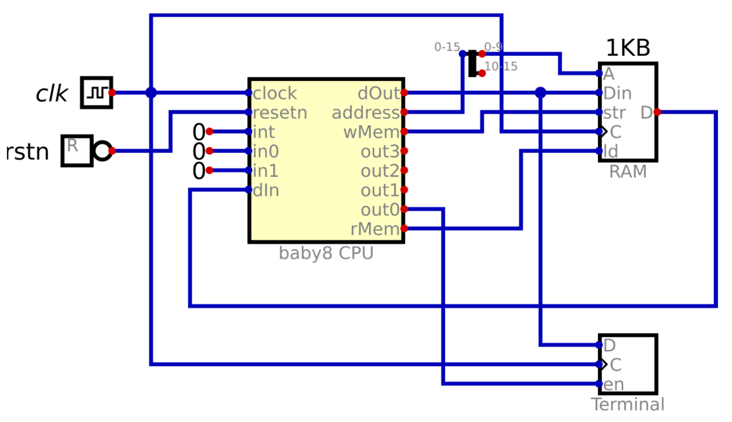
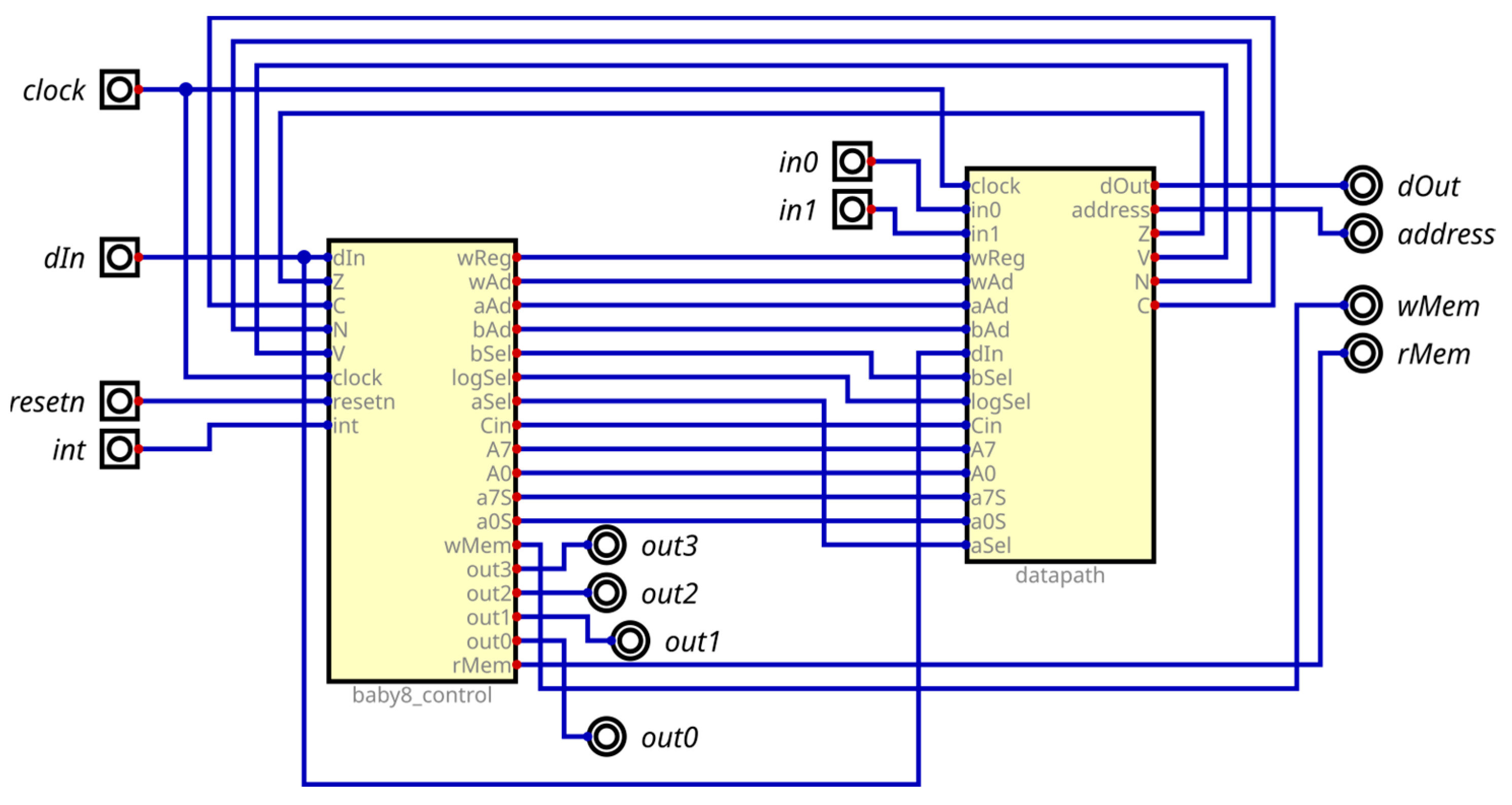
3.2. Custom Processor Design
An advanced digital design and simulation tool named DIGITAL, developed by Neemann, is employed for the design process. The Baby8 processor and its peripherals (RAM block and terminal) are shown in Figure 2, while its internal blocks are given in Figure 3.
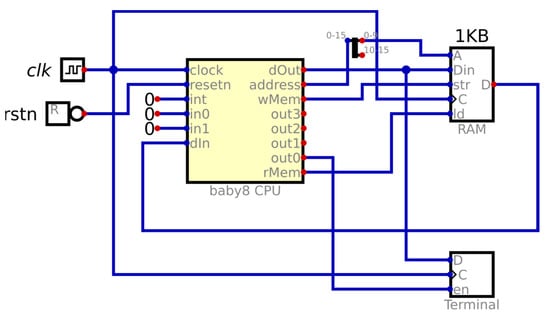
Figure 2.
The Baby8 CPU and its peripheral RAM block and terminal.
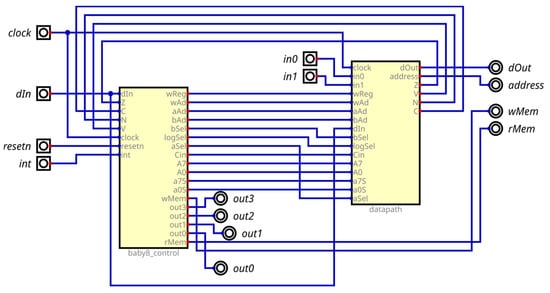
Figure 3.
The combination of the DATAPATH with the CONTROL UNIT forms the CPU.
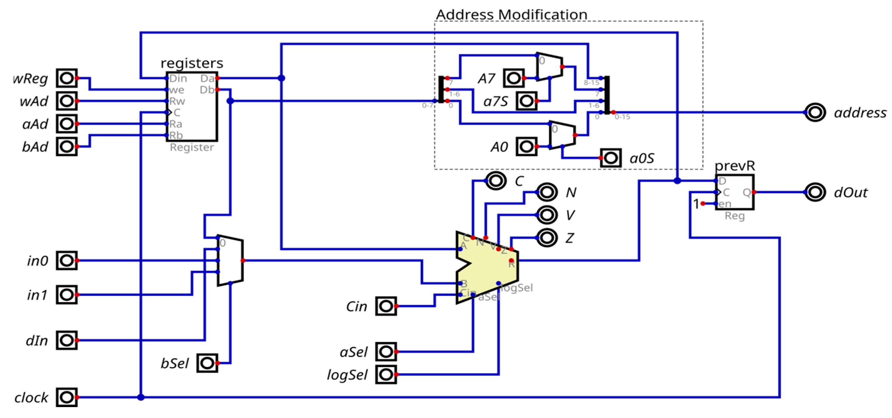
3.2.1. DATAPATH
The heart of the DATAPATH is the ALU (arithmetic logic unit). It can perform a logical operation (AND, OR, XOR, or NOT) between 8-bit inputs A and B, or modify input A. Figure 4 provides an in-depth view of the DATAPATH architecture and its internal components, including the ALU, register bank, multiplexers, address modifier (address modification), and data output register.

Figure 4.
The DATAPATH defines the logic to execute the instructions.
During the native data flow, operand B of the ALU typically originates from the output Db of the register bank. However, it may eventually come from memory or from one of the processor’s two input ports. In turn, the Da and Db outputs of the register bank together form a 16-bit address. Within the region of combinational logic circuits called address modification, the binary values of the addresses are processed. Bit 7 indicates whether the address is direct or indirect, while bit 0 signifies whether it should be used or not incremented.
The address from memory is not always desired, and it can be created from internal operands and/or ALU operations. Logical address modification circuits also serve this purpose. The first 127 memory addresses are allocated for normal programs, and the range between 128 and 255 is utilized by routines called interrupts. Additionally, a data output register is necessary to write to external memory, requiring 24 bits for this operation—16 address bits and another 8 data bits, concatenated at the clock edge, using 2 clock cycles for this operation. Although this operation slightly reduces performance, it enables the utilization of fewer FPGA hardware resources, aligning with the primary objective.
3.2.2. CONTROL UNIT
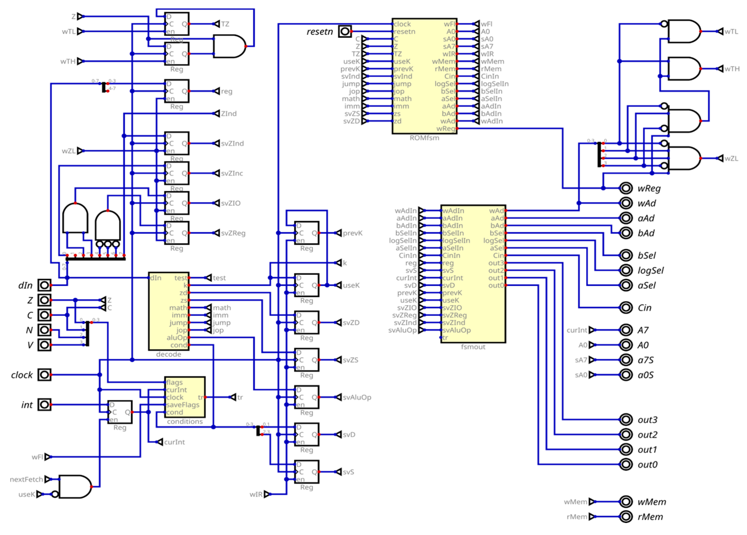
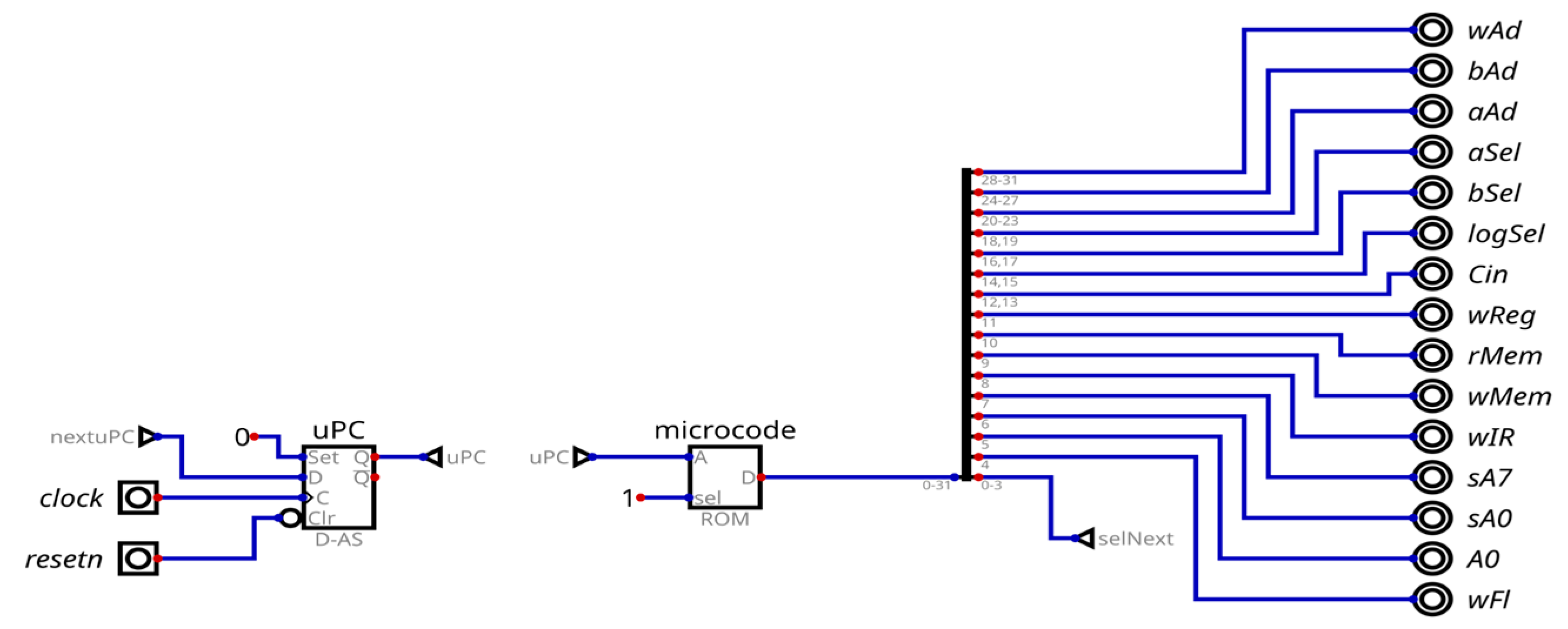
The core of the Baby8 processor control unit is the state machine defined by the ROMfsm block in Figure 5. Internally, it implements the internal ROM generating control signals for decoding (microcode), as specified in Figure 6 and Table 6. This connected finite state machine generates signals needed to use the data path to execute instructions.
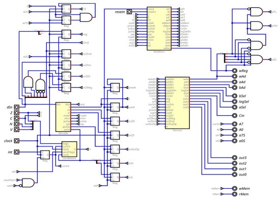
Figure 5.
A decodification combinatorial circuit inside a CONTROL unit.
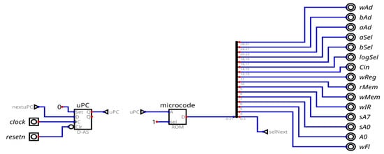
Figure 6.
Internal details of the ROMfsm block, containing the uPC microprogram counter register and the microcode ROM, whose contents are described in Table 6.
Table 6.
Internal ROM generates control signals by decoding OPCODES.
3.2.3. ALU
In the design of the ALU, several factors were meticulously considered to achieve a balance between performance and resource efficiency. The initial step involved defining the logical and arithmetic operations necessary for the application. Another critical aspect focused on the format of the operands to be manipulated.
Ultimately, priority was given to minimizing the area and optimizing the layout, with the reduction of the FPGA circuit area established as a primary project objective. This approach, tailored for FPGA implementation rather than TTL, led to specific decisions contributing to circuit reduction in this particular context. Choosing multiplexers at the input of the adders instead of at the output was one such decision. Motivated by the presence of a 6-input lookup table on the FPGA, this choice makes the circuit more compact for this specific case.
The ALU, showcased in Figure 7, was designed around an 8-bit adder, receiving two 8-bit data and a Cin (carry in) bit. This setup results in a 9-bit output, where 8 bits represent the operation result and 1 bit is the C (carry out).
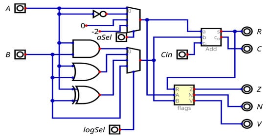
Figure 7.
The ALU combines two operands (A and B) in different ways according to the instructions.
The operations performed by the adder are determined by two multiplexers. The first multiplexer, in short, defines the arithmetic operations. Using the aSel selector, it is possible to choose the operand A, the inverse of A, 0, or -2.
The second multiplexer is mainly responsible for logical operations. Using the logSel selector, it is possible to choose between A and B, A or B, A or B, or just B.
In this way, with this simple circuit, we can perform all the necessary operations in our ALU. To perform a logical operation, we insert bit 0 into the first multiplexer, which will be added to the logic defined by the second multiplexer: AND, OR, or XOR. In this way, it is as if the adder were removed and the result of the logical operation was passed directly to the output.
Now, to perform arithmetic operations, we set the second multiplexer to send the operand B directly to the adder, while the first multiplexer can determine the operation. When we pass A directly, we perform an addition; when passing the inverse of A, we perform a subtraction, but to conduct this operation, we send 1 in Cin so that we have the two’s complement.
4. Results
All the results presented in Table 7 and Table 8 were evaluated using both scripts and data available by the authors in their Github repository. The results are divided into two tables, divided into RISC-V™ and non-RISC-V™ compatibility.
Table 7.
The ASIC and FPGA resources used by the RISC-V processors related to Baby8.
Table 8.
The ASIC and FPGA resources used by the non-RISC-V processors related to Baby8.
We show the main results classified as ASICs, NAND gates, and FPGAs. For the ASICs, we inform the maximum clock frequency, the power consumption, the efficiency, and the effective area of the CORE and DIE (DIE is a small block of semiconducting material on which a given functional circuit is fabricated).
For the NAND gates, we provide the plain number of gates used. And for the FPGAs, we inform the number of LUTs, registers, distributed memories, block memories, and DSP units used for each family of FPGA (Xilinx 7, Cyclone V, ICE 40, Gowin, and ECP 5).
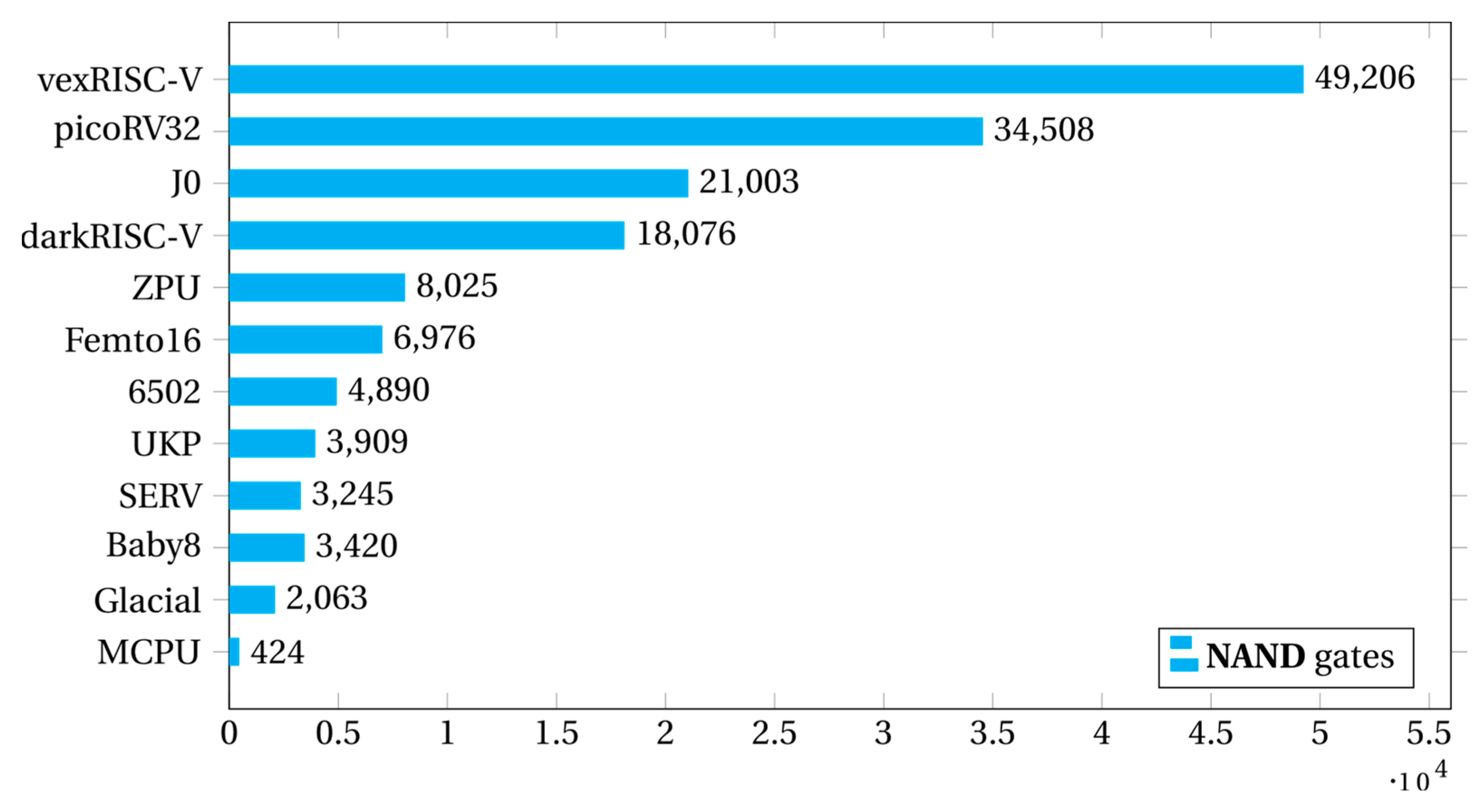
Figure 8 and Figure 9 show the total utilization of the DIE area and the number of NAND gates used by each processor.
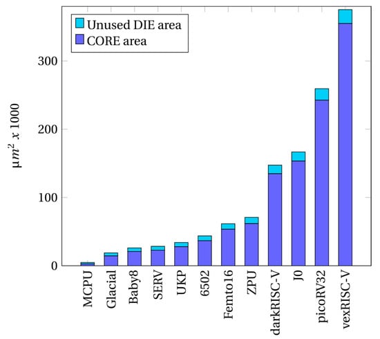
Figure 8.
The utilization of the total DIE area by the CORES processor.
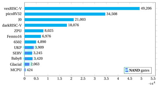
Figure 9.
Soft-core processor resource utilization for the ASICs/FPGAs based on the number of NAND gates.
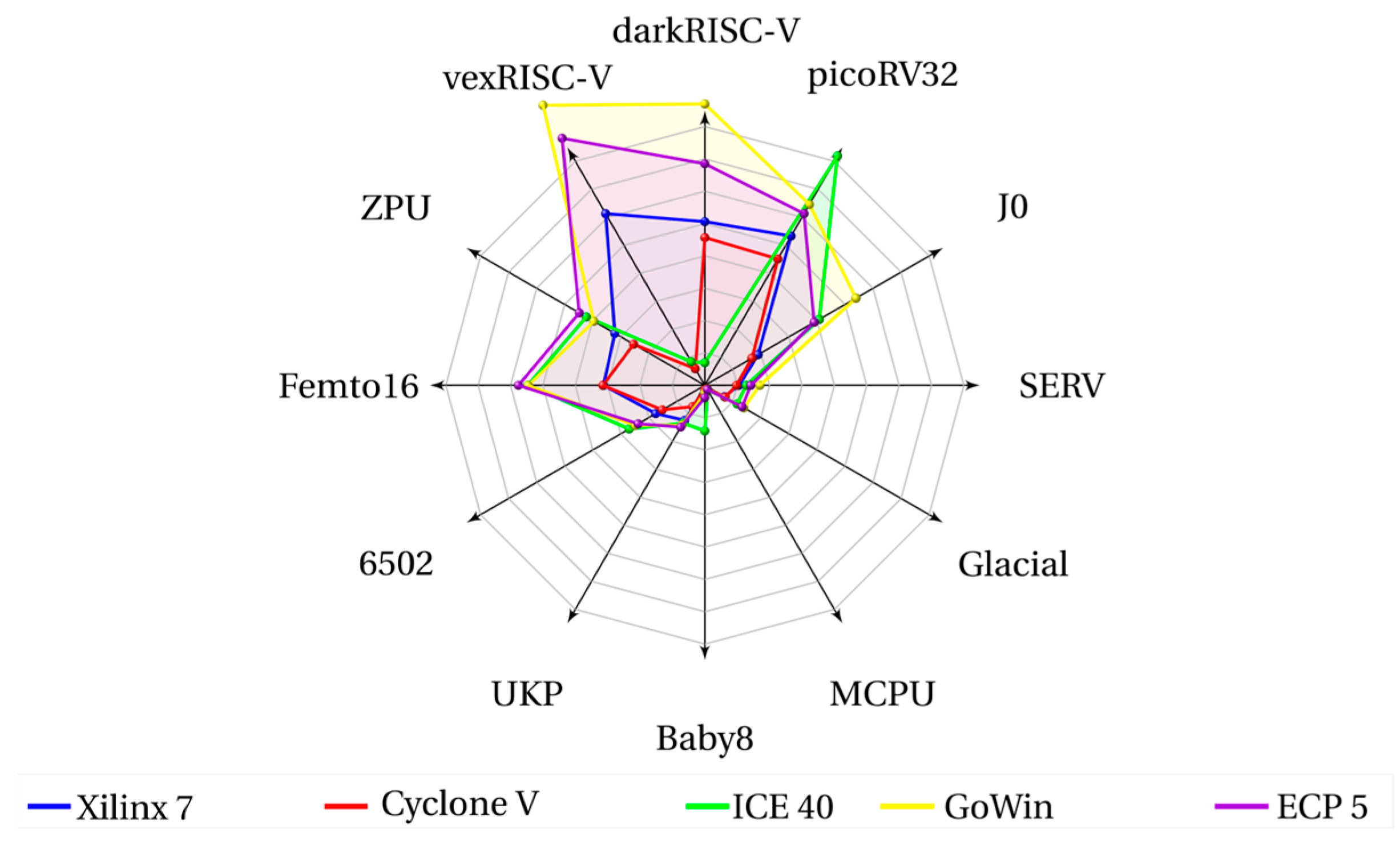
As shown in Figure 10, the number of LUTs can vary greatly depending on the chosen FPGA family for the same processor. The best use of resources is often linked to the improvement of development tools and the integration of the synthesis results generated into their own internal hardware. So a project decision cannot be based only on lower prices of the FPGA chips but also on their efficiency in the synthesis due to a greater use of resources based on the company’s technology.
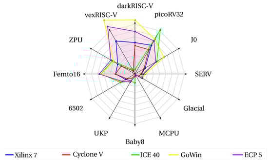
Figure 10.
The proportion of LUTs allocated per soft-core processor and per FPGA model.
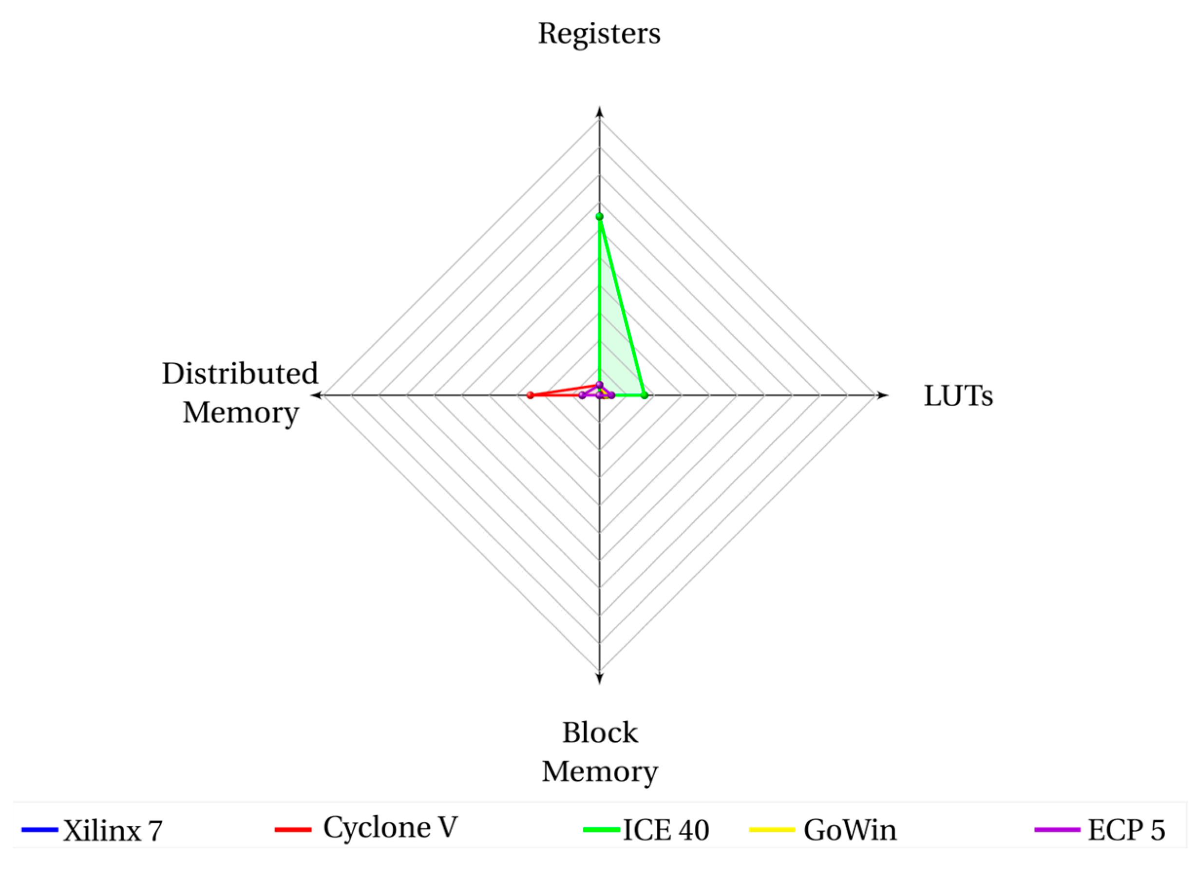
Figure 11 shows an extremely low use of FPGA resources for the I/O generic purpose processor Baby8 (that was exactly our initial goal in this project) in comparison with Figure 12 (darkRISCV) and Figure 13 (J0). Only the FPGA family ICE40 synthesized the Baby8 soft-core processor with a high use of resources.
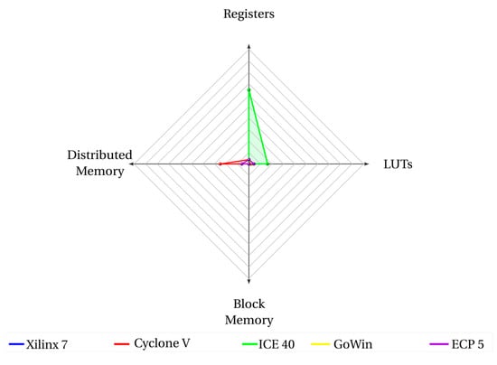
Figure 11.
Proportion of LUTs, registers, distributed memories, block memories, and DSP units allocated for the Baby8 processor per FPGA model.
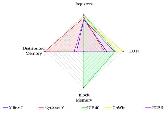
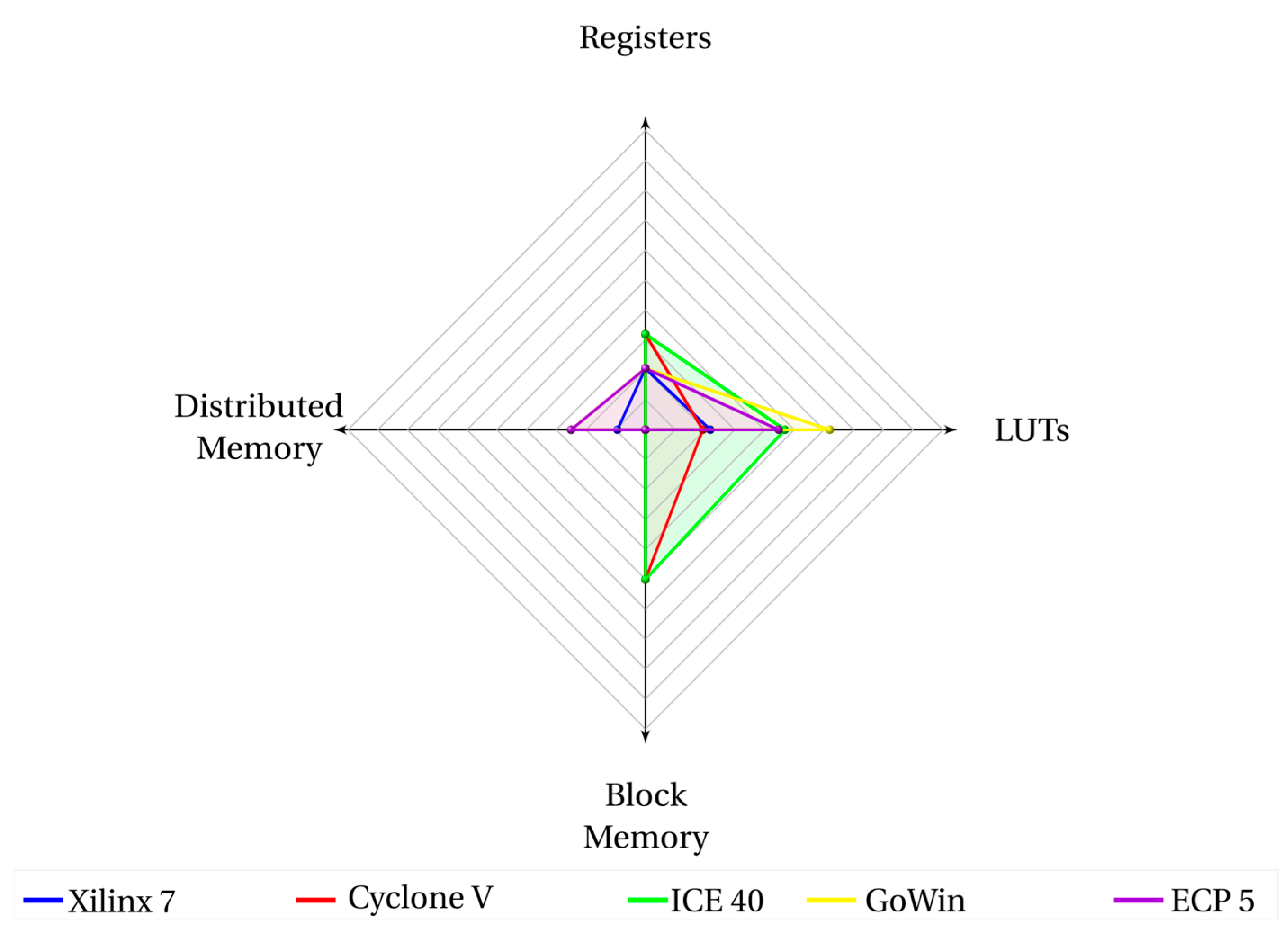
Figure 12.
Proportion of LUTs, registers, distributed memories, block memories, and DSP units allocated for the darkRISC-V processor per FPGA model.
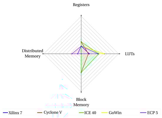
Figure 13.
Proportion of LUTs, registers, distributed memories, block memories, and DSP units allocated for the J0 processor per FPGA model.
One can notice that the same processor, darkRiscV (Figure 10), could be synthesized using more registers or more LUTs, depending on the FPGA family chosen.
The J0 processor is the only processor in this study that used FPGA DSP units for the FPGAs Xilinx 7, Cyclone V, and ECP 5. This is the reason why the FPGAs ICE40 and GoWin are consuming much more LUTs and registers than other ones in J0 on the radar plot of Figure 9. And despite the fact that the J0 processor consumes almost the same number of NAND gates as the darkRISCV processor (Figure 8), it consumes much less of the FPGA’s LUTs and registers due to the use of these FPGA’s DSP units.
4.1. Performance
Although performance is not a measure of resource utilization per se, resource contention certainly impacts directly on the final performance of a processor design.
As much as the objective of this paper is to develop a processor with low resource usage (in terms of internal components for FPGAs or even area for ASICs), we must show in this section a comparative analysis of the final performance of the developed processor compared to the others analyzed.
In Figure 14, we can see that our processor, Baby8, successfully achieves an average performance in maximum clock frequency as well as efficiency in power consumption among all other processors.
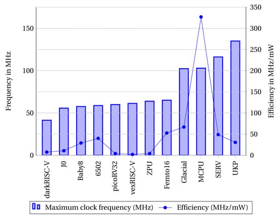
Figure 14.
Maximum clock frequency (MHz) vs. efficiency (MHz/mW) in an ASIC simulation with a 130 nm process and using the worst-case scenario: 1.6 volts at a temperature of 100 °C.
The frequency measurements were performed with OpenLane2 [11,12]. For each project, the OpenLane2 was configured to synthesize using the Sky130A PDK from Skywater and to use a 100 ns clock period (10 MHz) for the timing analysis.
This analysis was performed several times during the chip generation process, including after placement and routing. The timing analysis is done for the best case (low temperature and high supply voltage), the typical case, and the worst case (high temperature and low supply voltage). In addition, the analysis is performed for the minimum, nominal, and maximum delays for the components.
The limiting factor of how high the clock for the device can be is indicated by the worst case setup time slack for the maximum delay with high temperature and low supply voltage. Subtracting this value from the clock period gives us a higher clock than the original 10 MHz.
Synthesis is run again, and the same circuit should result, but the timing analysis will give a different setup slack in the worst case. It might seem that the new number would be zero, but there are several complicating factors, and the actual result will be smaller than the first time but still a positive value. The new number is subtracted from the new clock period, and the process is repeated. This allows a successive approximation to the actual maximum clock possible for each processor.
4.2. Layouts
The chip layouts were also produced using the Open Lane 2 tool [12], and the layouts of the smallest area (MCPU) and largest area (vexRISC-V) processors implemented are shown in Figure 15.
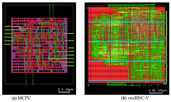
Figure 15.
The smallest area (MCPU) and largest area (vexRISC-V) chip layouts.
5. Discussion
Although our developed Baby8 soft-core processor achieves very good results in performance (~57 MHz) and energy consumption (~2 mW), we need to make sure it can meet the initially proposed requirements of using few FPGA internal resources.
In order to run this analysis, Baby8 results were compared with 6502 results, both implemented in the ICE40 FPGA family.
Baby8 uses practically half as many LUTs (285) as 6502 (544) in the same FPGA. It still uses a bit more registers—136—against 96 of 6502, but does not use any additional memory blocks, despite the fact that 6502 uses seven blocks or memory RAM.
Since both processors are very similar in all other aspects (both are CISC 8-bits with the same power consumption and the same maximum achieved frequency clock), we can consider that the Baby8 architecture could save up to half of the FPGA resources compared with the 6502 for the same features in the project.
6. Conclusions
Our developed soft-core processor architecture successfully achieves the goals of staying tiny and saving nearly half of the resources in FPGA implementation, keeping the same performance and power consumption as similar processors.
Author Contributions
Conceptualization, methodology, software: J.M.d.A.J.; formal analysis, investigation, data curation: M.G.; review, supervision, project administration and funding acquisition: O.H.A.J., M.R.C. and J.P.C. All authors have read and agreed to the published version of the manuscript.
Funding
This research was funded by the Brazilian Ministry of Science, Technology, and Innovations by providing five undergraduate grants in PMN-Design microelectronics program 2B, managed by the Eldorado Institute, Grant #SSJ14547.
Data Availability Statement
All data and software are available online at the authors’ Github repositories: https://github.com/jeceljr/baby8 and https://github.com/jeceljr/SoftCoreCompare accessed on 11 February 2024.
Acknowledgments
The Brazilian Ministry of Science, Technology, and Innovations, Eldorado Institute, Chandler Klüser, Alejandra Victoria Herrera, Hugo Puertas, Beatriz Aimee Teixeira Furtado Braga, Gabriel Valizi, Gabriel Victor Santana, Samuel Rocha Silva, Vinicius Caffeu, and Maximiliam Luppe.
Conflicts of Interest
The authors declare no conflict of interest.
Abbreviations
The following abbreviations are used in this manuscript:
| ALU | Arithmetic logic unit |
| ASIC | Application-specific integrated circuit |
| CISC | Complex instruction set computer |
| CPU | Central processing unit |
| FPGA | Field-programmable gate array |
| I/O | Input/output |
| RAM | Random access memory |
| RISC | Reduced instruction set computer |
References
- Glaser, J.; Wolf, C. Methodology and Example-Driven Interconnect Synthesis for Designing Heterogeneous Coarse-Grain Reconfigurable Architectures. In Proceedings of the Models, Methods, and Tools for Complex Chip Design; Haase, J., Ed.; Springer: Cham, Switzerland, 2014; pp. 201–221. [Google Scholar]
- Shah, D.; Hung, E.; Wolf, C.; Bazanski, S.; Gisselquist, D.; Milanovic, M. Yosys+nextpnr: An Open Source Framework from Verilog to Bitstream for Commercial FPGAs. In Proceedings of the 2019 IEEE 27th Annual International Symposium on Field-Programmable Custom Computing Machines (FCCM), San Diego, CA, USA, 28 April–1 May 2019; pp. 1–4. [Google Scholar] [CrossRef]
- Assumpção, J. Baby8. 2023. Available online: https://github.com/jeceljr/baby8 (accessed on 11 February 2024).
- Patterson, D.A.; Hennessy, J.L. Computer Organization and Design ARM Edition: The Hardware Software Interface; Morgan Kaufmann: Cambridge, MA, USA, 2016. [Google Scholar]
- Hiremath, S.; Chickerur, S.; Dandin, J.; Patil, M.; Muddinkoppa, B.; Adakoli, S. Open-source Hardware: Different Approaches to Softcore implementation. In Proceedings of the 2022 International Conference on Distributed Computing, VLSI, Electrical Circuits and Robotics (DISCOVER), Shivamogga, India, 14–15 October 2022; pp. 76–83. [Google Scholar] [CrossRef]
- SiFive. 2023. Available online: https://www.sifive.com/about (accessed on 11 February 2024).
- Heinz, C.; Lavan, Y.; Hofmann, J.; Koch, A. A Catalog and In-Hardware Evaluation of Open-Source Drop-In Compatible RISC-V Softcore Processors. In Proceedings of the 2019 International Conference on ReConFigurable Computing and FPGAs (ReConFig), Cancun, Mexico, 9–11 December 2019; pp. 1–8. [Google Scholar] [CrossRef]
- Gruin, A.; Carle, T.; Cassé, H.; Rochange, C. Speculative Execution and Timing Predictability in an Open Source RISC-V Core. In Proceedings of the 2021 IEEE Real-Time Systems Symposium (RTSS), Dortmund, Germany, 7–10 December 2021; pp. 393–404. [Google Scholar] [CrossRef]
- Coluccio, A.; Ieva, A.; Riente, F.; Roch, M.R.; Ottavi, M.; Vacca, M. RISC-Vlim, a RISC-V Framework for Logic-in-Memory Architectures. Electronics 2022, 11, 2990. [Google Scholar] [CrossRef]
- Copeland, B. TheManchester Computer: A Revised History Part 2: The Baby Computer. IEEE Ann. Hist. Comput. 2011, 33, 22–37. [Google Scholar] [CrossRef]
- Ghazy, A.A.; Shalan, M. OpenLANE: The Open-Source Digital ASIC Implementation Flow. 2020. Available online: https://woset-workshop.github.io/PDFs/2020/a21.pdf (accessed on 11 February 2024).
- Wang, H.; Li, T.; Li, Y.; Chen, L.; Sima, C.; Liu, Z.; Wang, B.; Jia, P.; Wang, Y.; Jiang, S.; et al. OpenLane-V2: A Topology Reasoning Benchmark for Unified 3D HDMapping. In Proceedings of the Thirty-Seventh Conference on Neural Information Processing Systems Datasets and Benchmarks Track, New Orleans, LA, USA, 10–16 December 2023. [Google Scholar]


Disclaimer/Publisher’s Note: The statements, opinions and data contained in all publications are solely those of the individual author(s) and contributor(s) and not of MDPI and/or the editor(s). MDPI and/or the editor(s) disclaim responsibility for any injury to people or property resulting from any ideas, methods, instructions or products referred to in the content. |
© 2024 by the authors. Licensee MDPI, Basel, Switzerland. This article is an open access article distributed under the terms and conditions of the Creative Commons Attribution (CC BY) license (https://creativecommons.org/licenses/by/4.0/).