Article

A Spiking LSTM Accelerator for Automatic Speech Recognition Application Based on FPGA

1
College of Engineering, Southern University of Science and Technology, Shenzhen 518055, China
2
Shenzhen Institute of Advanced Technology, Chinese Academy of Sciences, Shenzhen 518055, China
3
School of Computer Science and Technology, Huazhong University of Science and Technology, Wuhan 430074, China
*
Author to whom correspondence should be addressed.
Electronics 2024, 13(5), 827; https://doi.org/10.3390/electronics13050827
Submission received: 8 January 2024 / Revised: 7 February 2024 / Accepted: 16 February 2024 / Published: 21 February 2024
(This article belongs to the Section Artificial Intelligence Circuits and Systems (AICAS))

Abstract

:
Long Short-Term Memory (LSTM) finds extensive application in sequential learning tasks, notably in speech recognition. However, existing accelerators tailored for traditional LSTM networks grapple with high power consumption, primarily due to the intensive matrix–vector multiplication operations inherent to LSTM networks. In contrast, the spiking LSTM network has been designed to avoid these multiplication operations by replacing multiplication and nonlinear functions with addition and comparison. In this paper, we present an FPGA-based accelerator specifically designed for spiking LSTM networks. Firstly, we employ a low-cost circuit in the LSTM gate to significantly reduce power consumption and hardware cost. Secondly, we propose a serial–parallel processing architecture along with hardware implementation to reduce inference latency. Thirdly, we quantize and efficiently deploy the synapses of the spiking LSTM network. The power consumption of the accelerator implemented on Artix-7 and Zynq-7000 is only about 1.1 W and 0.84 W, respectively, when performing the inference for speech recognition with the Free Spoken Digit Dataset (FSDD). Additionally, the energy consumed per inference is remarkably efficient, with values of 87 µJ and 66 µJ, respectively. In comparison with dedicated accelerators designed for traditional LSTM networks, our spiking LSTM accelerator achieves a remarkable reduction in power consumption, amounting to orders of magnitude.

1. Introduction

Automatic Speech Recognition (ASR), which converts spoken words into text, has been a prominent research area for decades [1,2]. Its primary objective is the real-time understanding of continuous speech. Nowadays, with the assistance of neural networks [3], ASR technology has been widely integrated into many commercial products like ‘Google Now’ (Google), ‘Siri’ (Apple), and ‘Xiaodu’ (Baidu). The activation of these ASR systems relies on specific wake-up keywords (e.g., ‘Ok Google’, ‘Hey Siri’, and ‘XiaoduXiaodu’). Mobile, audio systems, and other wearable devices often maintain an ‘always-on’ mode, continuously listening for keywords or performing wake-up keyword detection tasks without a dedicated start control. Minimizing the energy consumed by this wake-up keyword detection task is significant in these battery-powered systems. In the context of a mobile phone, let us consider that the battery operates at a voltage of 3.6 V, and the power consumption of the ASR system is 10 W. For a runtime of one hour, the required battery capacity can be calculated as 10 W/3.6 V × 1 h = 2780 mAh. However, typical phone batteries have capacities ranging from 3000 mAh to 5000 mAh. Therefore, the 10 W power consumption is deemed unacceptable, and efforts should be made to minimize it.
One of the widely employed neural networks for speech recognition is the Recurrent Neural Network (RNN), which uses an internal state (memory) to process arbitrary sequences of inputs such as speech. However, traditional RNNs encounter gradient vanishing and explosion during training, especially for tasks like speech recognition involving long sequences [4,5]. Long Short-Term Memory (LSTM) [6] is then developed to address these challenges by employing the forget gate within the LSTM cell to discard irrelevant information. However, due to the extensive matrix–vector multiplication operations within the neural network architecture of LSTM, its execution remains both computation intensive and memory intensive, even in the inference phase [7]. To optimize LSTM for lightweight applications, various technologies have been introduced to save computation, as well as memory footprint [8,9,10]. For example, a model compression technique including parameter pruning and quantization is proposed in ESE to compress the dense weight matrices into sparse ones [8]; C-LSTM is a structured compression technique that not only reduces the LSTM model size but also eliminates the irregularities of computation and memory accesses [10]; The weight parameter generation method based on vector construction has been proposed in [11] to achieve a high compression ratio and produce less precision attenuation. While compression techniques aid in reducing model size and computational requirements, the substantial volume of multiplications and nonlinear functions (e.g., sigmoid and tanh) within the LSTM cell remains a significant energy bottleneck when deploying LSTM networks in battery-powered edge devices.
Inspired by the biological brain, an alternative approach to reducing computational complexity and energy consumption in traditional neural networks, such as LSTM, involves using addition and comparison instead of multiplication and nonlinear functions. Many studies have demonstrated the energy-efficient features of spiking neural networks (SNNs) in both algorithmic approaches [12,13,14] and hardware implementations [15,16,17,18,19,20,21]. Most of these studies primarily focus on spiking convolutional neural networks (S-CNN) and spiking fully connected neural networks (S-FC). On the other hand, Rezaabad et al. proposed a spiking LSTM network (S-LSTM) in which the output of sigmoid gates in each unit is rounded to ‘spike’ or ‘no-spike’ [22]. However, this proposed approach has not been implemented in hardware. In other related works [23,24], the researchers focused on mapping traditional LSTM on neuromorphic chips or hardware accelerators rather than specifically tailored accelerators for spiking LSTM. Specifically, ref. [23] introduces approximation techniques that facilitate the mapping of traditional LSTM to TrueNorth [15], an SNN chip. Arjun et al. [24] employ after-hyperpolarizing (AHP) currents to emulate the function of traditional LSTM cells, realized through a two-compartment version of the LIF neuron model using Intel’s Loihi chip [16].
In this work, we present an FPGA-based hardware accelerator to accelerate the spiking LSTM network. The rest of this paper is organized as follows. Section 2 gives a brief introduction of the traditional LSTM network and spiking LSTM network. In Section 3, the architecture and circuit implementation of the low-power spiking LSTM accelerator are presented. The Spiking LSTM accelerator is further evaluated and compared with some related works in Section 4. Section 5 concludes this paper.

2. Spiking LSTM Network

2.1. Traditional LSTM Network

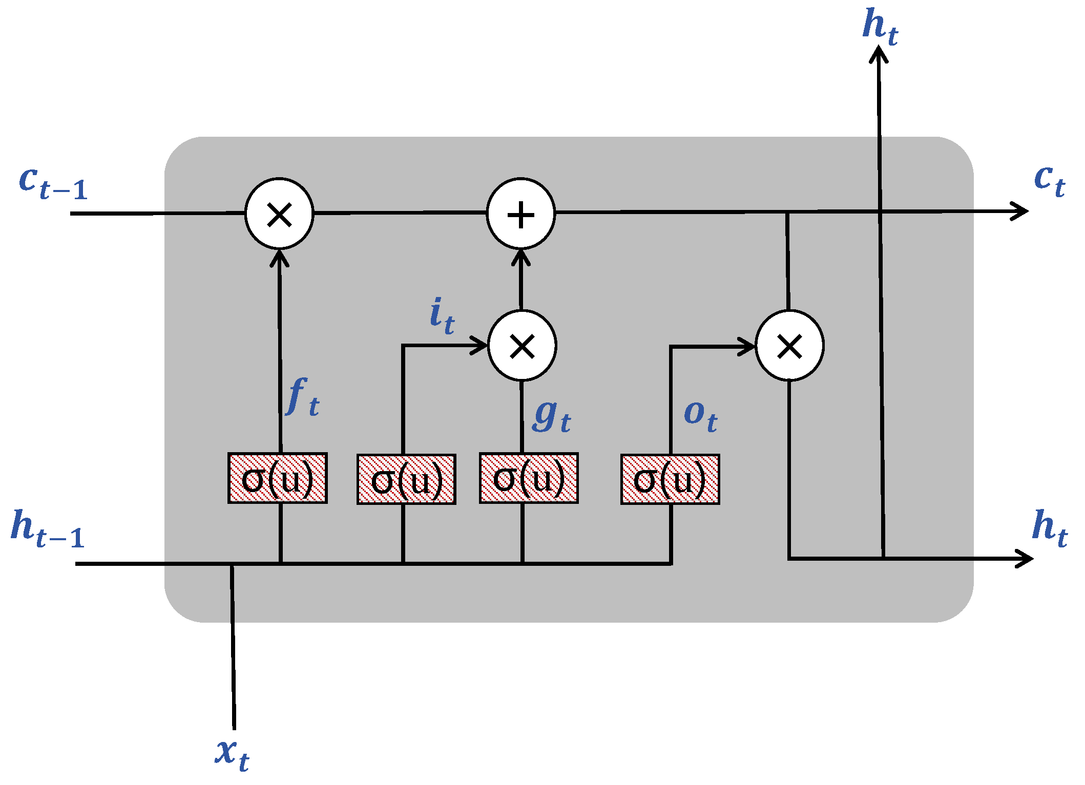
Traditional LSTM [6] is a typical gated RNN. Unlike the RNN cell, the LSTM cell introduces three gates (i.e., input gate i t , output gate o t and forget gate f t ) to regulate the flow of information into and out of the LSTM cell, as shown in Figure 1. These gates effectively address the vanishing gradient problem faced by the RNN network. The state update equations for the traditional LSTM cell are expressed by Equation (1a–f):
f t = σ ( W x f x t + W h f h t 1 + b f )
i t = σ ( W x i x t + W h i h t 1 + b i )
g t = σ ( W x g x t + W h g h t 1 + b g )
c t = f t c t 1 + i t g t
o t = σ ( W x o x t + W h o h t 1 + b o )
h t = o t t a n h ( c t )
The forget gate f t determines what information to discard from a previous state, while the input gate i t decides which part of new information to store in the current state. The cell-state vector c t is determined by the forget gate f t and input gate i t . The output gate o t controls which part of the information in the current state to output h t according to the previous and current states. In contrast to RNN, LSTM introduces the cell-state vector c t to retain current state information for computing the cell’s output at the subsequent time step. Unlike RNNs, which replace the current state with new input information, LSTM maintains relevant information from the previous time step. This enables LSTM networks to preserve long-term dependencies, enhancing their ability to make predictions. Consequently, LSTM achieves higher prediction accuracy for tasks with long sequences of data, such as speech recognition.

2.2. Spiking LSTM Network

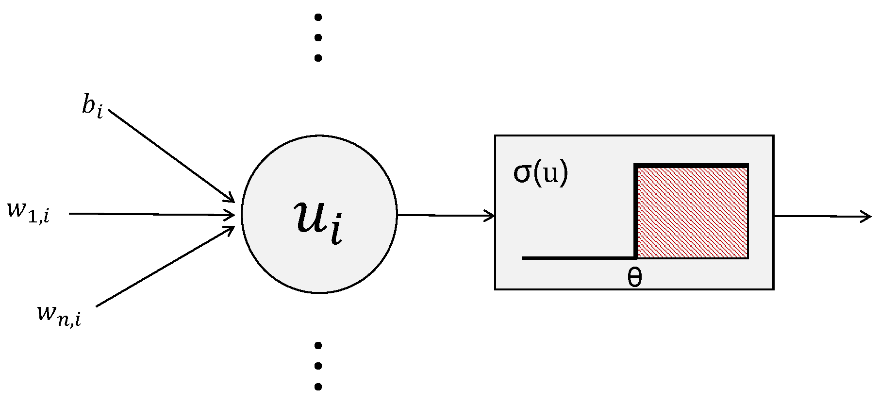
The spiking LSTM network designed for speech recognition comprises 200 spiking LSTM cells in the hidden layer and 10 spiking fully connected (FC) neurons in the output layer. It processes the input speech signal to classify it into 10 classes. In the spiking LSTM cell [22], depicted in Figure 2, spike activation is employed for individual neurons instead of traditional nonlinear functions like sigmoid or hyperbolic tangent. These conventional nonlinear functions inherently demand high energy and hardware costs. Conversely, spike activation regulates each neuron’s output to ‘0’ or ‘1’, avoiding the energy- and hardware-intensive matrix multiplications. This spike activation function is extensively used in spiking neural networks, which will generate or fire a ‘spike’ or ‘1’ if the membrane potential exceeds a predefined threshold at each time step. As demonstrated in Figure 3, when a neuron receives a ‘spike’, the membrane potential u i varies based on its weights ( w 1 , i w n , i ), with the bias b i added to u i before spike generation. σ ( u ) is the spike activation function, mapping the membrane potential of a neuron u to a ‘spike’ if it exceeds the threshold value θ .
Similar to traditional LSTM, the key difference lies in the adoption of spike activation functions in the spiking LSTM. Given a set of spiking inputs x 1 , x 2 , , x t , the state updates of the spiking LSTM are expressed by Equation (2a–f):
f t = σ 1 ( W x f x t + W h f h t 1 + b f )
i t = σ 1 ( W x i x t + W h i h t 1 + b i )
g t = σ 2 ( W x g x t + W h g h t 1 + b g )
c t = f t c t 1 + i t g t
o t = σ 1 ( W x o x t + W h o h t 1 + b o )
h t = o t c t
where ⊙ means element-wise multiplication. W and b denote weight matrices (e.g., W x i is the matrix of weights from the input to the input gate) and bias vectors, respectively. Additionally, σ 1 and σ 2 are spike activations with a distinct threshold value, denoted as θ 1 and θ 2 , respectively. When a neuron generates a spike, the output of the neuron is ‘1’; otherwise, the output of the neuron is ‘0’;. It is important to note that the expression f t c t 1 + i t g t can take on values of 0, 1, or 2. We threshold this output to ‘1’ when it is 1 or 2.

2.3. Training Methodology for Spike LSTM

There are various methodologies for training spiking neural networks. For example, the conversion-based methodology converts a trained artificial neural network to a spiking neural network using weight scaling and normalization [25]. The spike-based backpropagation methodology is similar to backpropagation for artificial neural networks, where a differentiable alternative is required to make error derivatives calculable in spiking neural networks [22,26]. Spike-time-dependent plasticity (STDP) is a bio-inspired unsupervised learning methodology for spiking neural networks, but it is challenging to benchmark [27]. We adopt the spike-based backpropagation methodology for the spiking LSTM [22].
As illustrated in Figure 3, the function σ ( μ ) represents a spike activation, which is nondifferentiable and can potentially disrupt the backpropagation of error. To mitigate this issue, an alternative approximation is employed. The derivative of σ ( μ ) is provided in Equation (3), where f denotes the probability density function, and | u | | θ | signifies the difference between the neuron’s membrane potential and the threshold. This derivative can be effectively relaxed using a Gaussian distribution.
σ ( u ) = lim δ 0 0 E [ σ ( u + δ 0 ) ] = lim δ 0 0 [ f ( δ + δ 0 ) δ 0 × 1 δ 0 + ( 1 f ( δ + δ 0 ) δ 0 ) × 0 ] = f ( δ ) = f ( | u | | θ | )
The output layer of the spiking LSTM network is defined as y = softmax ( w y h t + b y ) , (hardmax replacing softmax during the inference phase to enhance efficiency). The derivative of the loss function for this output layer is expressed in Equation (4), where y label represents the label.
L y t = y t y label
Combining Equations (2a–f) and (4), the weights are updated according to the following equations:
Δ w y = t h t T L y t
Δ w o , x = t σ 1 ( Δ 1 [ w o , h h t 1 + w o , x x t + b o , h + b o , x ] ) x t 1 L o t
Δ w o , h = t σ 1 ( Δ 1 [ w o , h h t 1 + w o , x x t + b o , h + b o , x ] ) h t 1 L o t
Δ w i , x = t σ 1 ( Δ 1 [ w i , h h t 1 + w i , x x t + b i , h + b i , x ] ) x t 1 L i t
Δ w i , h = t σ 1 ( Δ 1 [ w i , h h t 1 + w i , x x t + b i , h + b i , x ] ) h t 1 L i t
Δ w g , x = t σ 2 ( Δ 2 [ w g , h h t 1 + w g , x x t + b g , h + b g , x ] ) x t 1 L g t
Δ w g , h = t σ 2 ( Δ 2 [ w g , h h t 1 + w g , x x t + b g , h + b g , x ] ) h t 1 L g t
Δ w f , x = t σ 1 ( Δ 1 [ w f , h h t 1 + w f , x x t + b f , h + b f , x ] ) x t 1 L f t
Δ w f , h = t σ 1 ( Δ 1 [ w f , h h t 1 + w f , x x t + b f , h + b f , x ] ) h t 1 L f t
During the training phase, the initial values of all weights are drawn from a standard normal distribution, while the initial values of biases are set to zero. We employ the Adam optimizer [28] for training the spiking LSTM network using a learning rate of 0.001. The exponential decay rates for the moment estimates are set to β 1 = 0.9 and β 2 = 0.999 .

2.4. Spike Encoding

We illustrate the performance of the proposed spiking LSTM accelerator on the Free Spoken Digit Dataset (FSDD) [29]. FSDD is an open speech dataset consisting of recordings of English spoken digits ‘0’∼‘9’, sampled at 8 kHz. It comprises recordings of numbers spoken by four different speakers, with a total size of 2000 (each speaker contributing 500 recordings). To effectively represent each sample for classifying, we transform samples using 1D wavelet scattering transform. After applying this preprocessing, each sample becomes a 1D vector size of 336 coming from 10 different classes.
Since spiking LSTM networks process signals in the form of spikes, it is essential to encode the input signal like speech into spikes. We convert speech samples into ON- and OFF-event-based values using Poisson sampling, which utilizes the Poisson distribution. The spike encoding scheme is depicted in Figure 4. The Poisson distribution is suitable for describing the number of random events occurring within a unit time, which aligns well with the nature of spike firing. The Poisson distribution can be defined as follows: within a unit time, events occur on average λ times, with equal probability and mutual independence among events. The probability distribution of events occurring k times within a unit time is mathematically expressed as
P ( X = k ) = e λ λ k k !
where λ represents the average occurrence rate of random events within a unit of time.
This encoding process resulted in the transformation of the speech signal into a sequence containing 336 spikes x [ 335 : 0 ] . As illustrated in Figure 4, this sequence is divided into eight segments x 0 [ 41 : 0 ] x 7 [ 41 : 0 ] , each consisting of a series of 42 spikes. These segments are sequentially input into the system for computation over eight time steps.

3. Proposed Spiking LSTM Accelerator

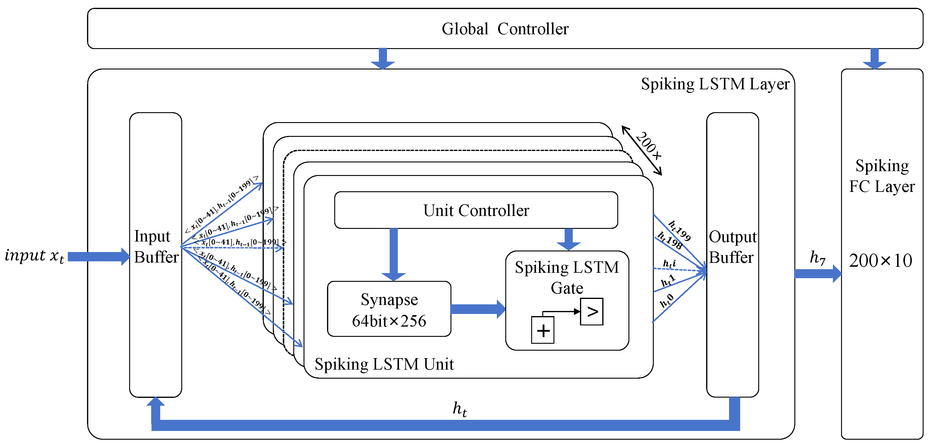
The overall architecture of the proposed spiking LSTM accelerator for spiking LSTM networks’ inference is shown in Figure 5. It mainly consists of the spiking LSTM layer responsible for running hidden layers and the spiking FC layer utilized for the output layer. The global controller manages weight and bias loading into synapse memory and controls the input spike train into the spiking LSTM layer, along with controlling the output speech recognition result.

3.1. Circuit Implementation of the Spiking LSTM Layer

There are 200 spiking LSTM units within the spiking LSTM layer, operating in parallel to accelerate the network’s inference. Each unit comprises a spiking LSTM gate, synapse, and unit controller. The spiking LSTM gate performs computations involved in the state update Equation (2a–f), while the synapse stores the network’s weights.

3.1.1. Low-Cost Spiking LSTM Gate

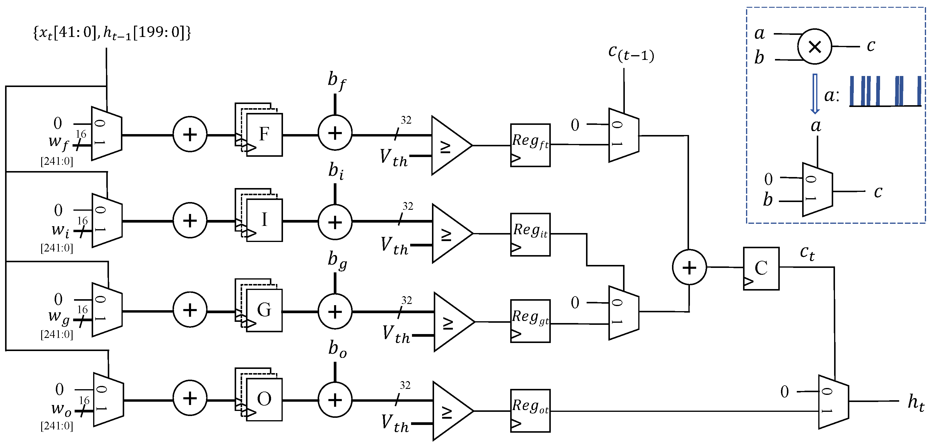
The conventional implementation of the spiking LSTM gate typically involves multipliers due to multiplication operations in the state update Equation (2a–f), leading to high energy and hardware costs. However, considering that the operands of these multiplications, such as x t , h t 1 , c t , c t 1 , g t , and o t , are ‘spike’, which are ‘0’ or ‘1’, we can employ multiplexers (MUXs) instead of multipliers to perform the multiplication operation. Consequently, we propose a low-cost spiking LSTM gate, depicted in Figure 6, wherein the high-cost multipliers are substituted with low-cost MUXs. The power consumption of a MUX could be tens of times lower than that of the multiplier [30].
The unit controller loads the weights from the synapse to the spiking LSTM gate only when the input spike of { x t [ 41 : 0 ] , h t 1 [ 199 : 0 ] } is ‘1’. By doing so, we can save on the weight load operation and reduce energy consumption when the input is ‘0’. Thanks to the low cost of MUXs and the data independence among Equation (2a–c,e), it is advantageous to implement four duplicate circuit blocks comprising MUX, accumulator, adder, register, and comparator. This setup enables the parallel computation of f t , i t , g t , and o t , and their accumulation results are stored in the register R e g f t , R e g i t , R e g g t , and R e g o t , respectively, as shown in Figure 6. Additionally, two MUXs and one adder are implemented to perform Equation (2d) and obtain c t . In the final output of each unit, h t is selected between o t and ‘0’ using a MUX controlled by c t .

3.1.2. Serial–Parallel Processing

The proposed accelerator performs the spiking LSTM network in serial–parallel processing style. The serial processing arises from segmenting each speech signal into eight segments x t [ 41 : 0 ] : x 0 [ 41 : 0 ] x 7 [ 41 : 0 ] , as discussed in Section 2.4. Each segment needs to be processed serially due to data dependence among the eight segments. On the other hand, during each segment processing phase, parallel processing remains available, occurring on two levels: firstly, among the 200 spiking LSTM units depicted in Figure 5, and secondly, within each unit where the state of f t , i t , g t , and o t are updated in parallel, as shown in Figure 6. Compared with the design with one spiking LSTM unit, this serial–parallel processing architecture theoretically reduces the latency by 200 × .
Specifically, the timing diagram illustrating the serial–parallel processing for the spiking LSTM layer is shown in Figure 7. The spiking LSTM layer conducts computations over eight time steps for the recognition of each speech signal, comprising eight segments x t [ 41 : 0 ] : x 0 [ 41 : 0 ] x 7 [ 41 : 0 ] . At each time step t, the current segment x t [ 41 : 0 ] —comprising 42 spikes—and the processing result of the previous time step of 200 spiking LSTM cells (i.e., h t 1 [ 199 : 0 ] ) are fed into each spiking LSTM unit for computation in the current time step. For the initial time step’s computation, h t 1 [ 199 : 0 ] is set to 0. The spiking LSTM layer generates the final result, h 7 [ 199 : 0 ] , during the last time step (i.e., the eighth time step), which is then forwarded to the spiking fully connected output layer.

3.2. Circuit Implementation of the Spiking Fully Connected Layer

The circuit implementation of the spiking fully connected (FC) layer is demonstrated in Figure 8. Since the output of the spiking LSTM layer is a vector with 200 elements ( h 7 [ 199 : 0 ] ) and our target dataset involves 10 classes in the FSDD, this spiking FC layer is configured with 10 neurons and 200 × 10 synapses or weights. To optimize hardware utilization, the 10 neurons are time-multiplexed using a single physical neuron. The synapse and Neuron_Mem are SRAM components employed to store weights and membrane potentials, respectively. The controller checks the element values within h 7 [ 199 : 0 ] and selectively loads the corresponding weights from the synapse for computation only when the element is ‘1’. Once the spiking FC layer completes the computation for all elements in h 7 [ 199 : 0 ] , the index of the neuron with the maximum membrane potential determines the recognized speech result for FSDD. The postprocessing is achieved by iteratively comparing the membrane potentials of the 10 neurons using a 64-bit comparator, as depicted in Figure 8.

3.3. Hardware-Friendly Synapse Deployment

While LSTM gates address the vanishing gradient issue that within RNNs, they require much more weights than fully connected networks, e.g., eight weights in each cell, including W x f [ 41 : 0 ] , W h f [ 199 : 0 ] , W x i [ 41 : 0 ] , W h i [ 199 : 0 ] , W x g [ 41 : 0 ] , W h g [ 199 : 0 ] , and W x o [ 41 : 0 ] , W h o [ 199 : 0 ] . Therefore, it is crucial to minimize the size of the required weights and optimize for deploying on hardware. We quantize the weights of the spiking LSTM network and then efficiently deploy them onto SRAM.

3.3.1. Weight Quantization

We employ a symmetric quantization strategy that quantizes weights in a manner that preserves symmetry around zero. This approach reduces the number of bits needed to represent the weights while minimizing distortion. Specifically, we utilize the torch.quantize_per_tensor [31] provided by PyTorch for implementing this symmetric quantization. The quantization formula is as follows:
Q = r o u n d ( o r i g i n a l _ w e i g h t z e r o _ p o i n t s c a l e )
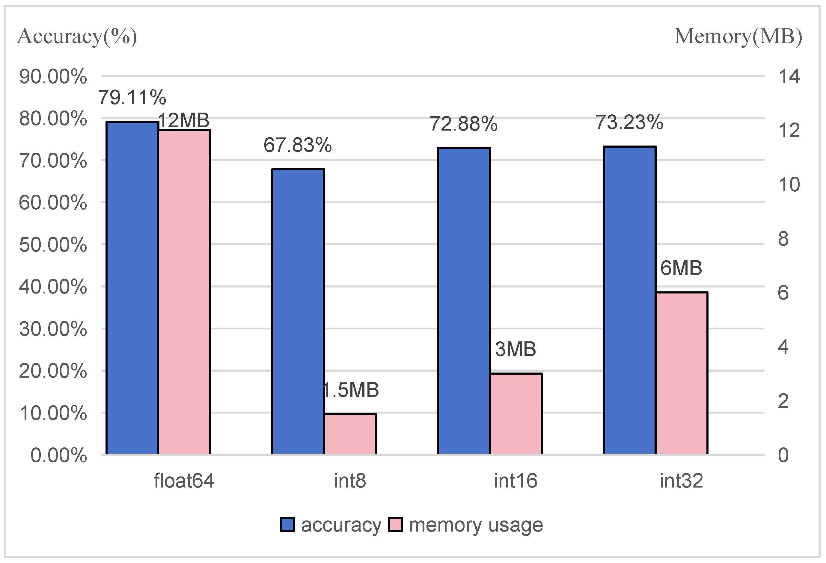
We performed quantization on the 64-bit floating-point (float64) weights of the spiking LSTM layer, converting them into fixed-point numbers represented by 8-bit (int8), 16-bit (int16), and 32-bit (int32) formats. The inference accuracy and memory footprint for each quantization level are depicted in Figure 9. Meanwhile, the weights of the spiking FC layer are quantized into 32-bit (int32) representations, as they only require approximately 8 kB of memory. From Figure 9, it can be seen that a significant decrease in inference accuracy is noted when the weights are quantized to int8. Conversely, quantizing the weights to int16 and int32 demonstrates less than a 0.5% accuracy difference. Therefore, we chose int16 quantization instead of int32 to reduce the memory footprint. The required memory footprint for the spiking LSTM layer is approximately 3 MB. Compared with the trained model, which requires a 12 MB memory footprint, int16 quantization saves 4 × the storage.

3.3.2. Memory Organization for Weight

We utilize 64-bit × 256 SRAM blocks for the spiking LSTM layer’s weight storage. In the spiking LSTM layer illustrated in Figure 10a, 16-bit weights within a single spiking LSTM cell are organized into a group with 64 bits, either W x f , W x i , W x g , W x o or W h f , W h i , W h g , W h o . These organized 64-bit data are stored at the same SRAM address. When a spike with a value of ‘1’ occurs, the four weights within the same spiking LSTM cell can be concurrently loaded for parallel computation. The 32-bit weights of the spiking FC layer are stored in a 32-bit × 2048 SRAM. These weights are arranged based on the neuron order. For example, the weights of the first neuron are located in the address of 0∼199.

4. Experiments and Results

4.1. Experimental Setup

We developed the proposed spiking LSTM accelerator using SystemVerilog, conducted synthesis and implementation through Vivado 2022, and performed evaluations on Xilinx Artix-7 XC7A200t, San Jose, CA, USA and Zynq-7000 XC7Z020 FPGAs, both manufactured with a 28 nm process. For comparison, we employed the Intel(R) Xeon(R) Silver 4214R CPU and the NVIDIA A100 GPU. The inference accuracy for speech recognition is evaluated with the Free Spoken Digit Dataset (FSDD) [29].

4.2. Experimental Results

Table 1 and Table 2 provide detailed hardware resource utilization when implementing the proposed spiking LSTM accelerator on the Artix-7 XC7A200t and Zynq-7000 XC7Z020 FPGA, respectively, operating at a clock frequency of 120 MHz. The power consumption of Artix-7 and Zynq-7000 is only about 1.1 W and 0.84 W, respectively, when performing the inference for speech recognition with FSDD. If the spiking LSTM accelerator is implemented in an advanced process like 10 nm, the power consumption may be reduced by up to 10 × , making it more suitable for battery-powered systems. The latency and accuracy are 78.93 µs and 72.88%, respectively. Due to insufficient BRAM resources on the Zynq-7000 XC7Z020 for spiking LSTM, 256 out of 17400 LUTRAM have been utilized in this case. Furthermore, implementation on the Zynq-7000 XC7Z020 results in lower power consumption, primarily due to its smaller scale compared witj the Artix-7 XC7A200t.
Figure 11 illustrates the algorithmic workflow for obtaining the inference model. Firstly, a spiking LSTM network with a structure of 42-100-10 is developed. Then, it is trained using a spike-based backpropagation training methodology. After training, the trained model is obtained. Lastly, symmetric quantization is adopted to quantize the trained model, resulting in the final inference model.

4.3. Comparison with Other Works

4.3.1. Comparison with CPU and GPU

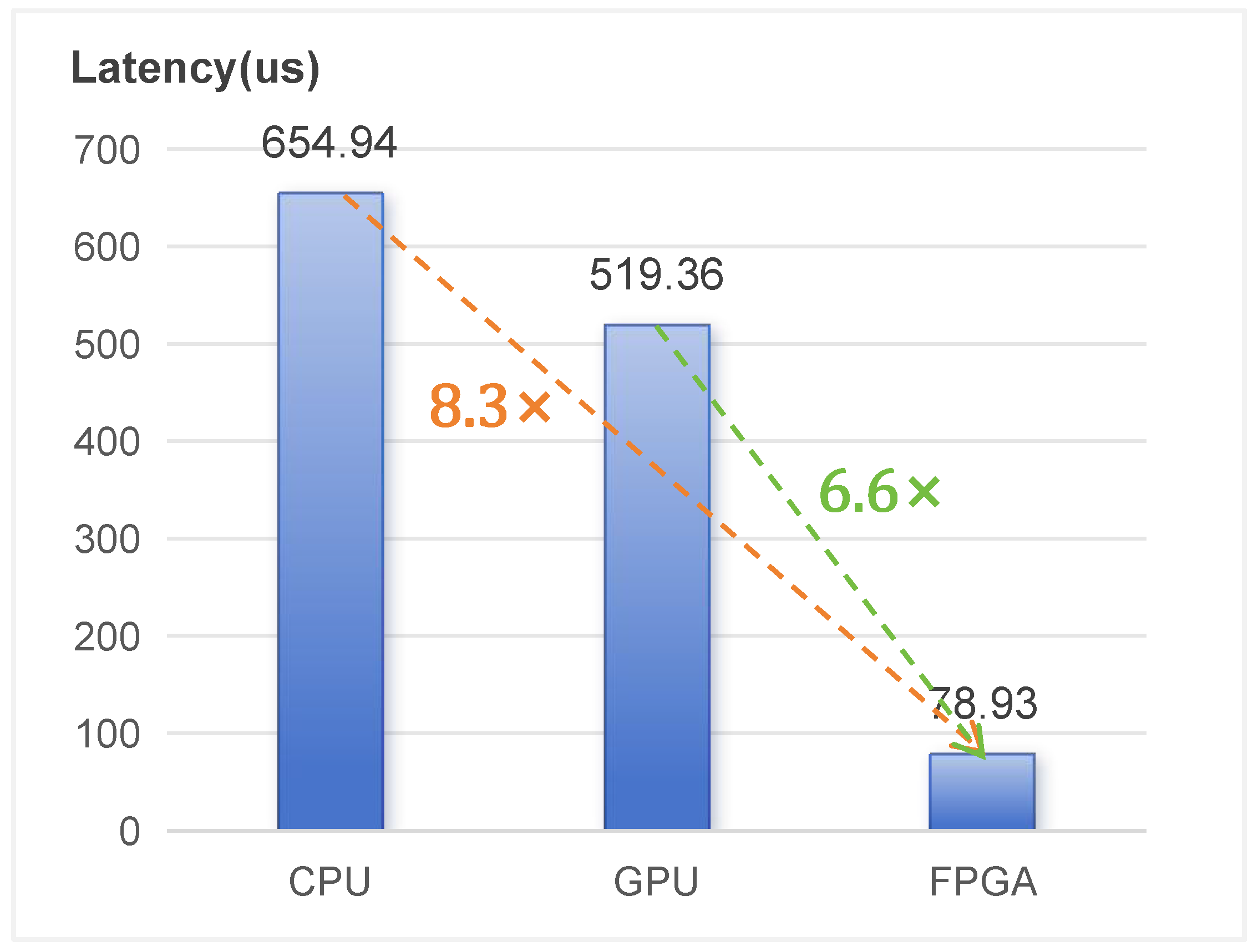
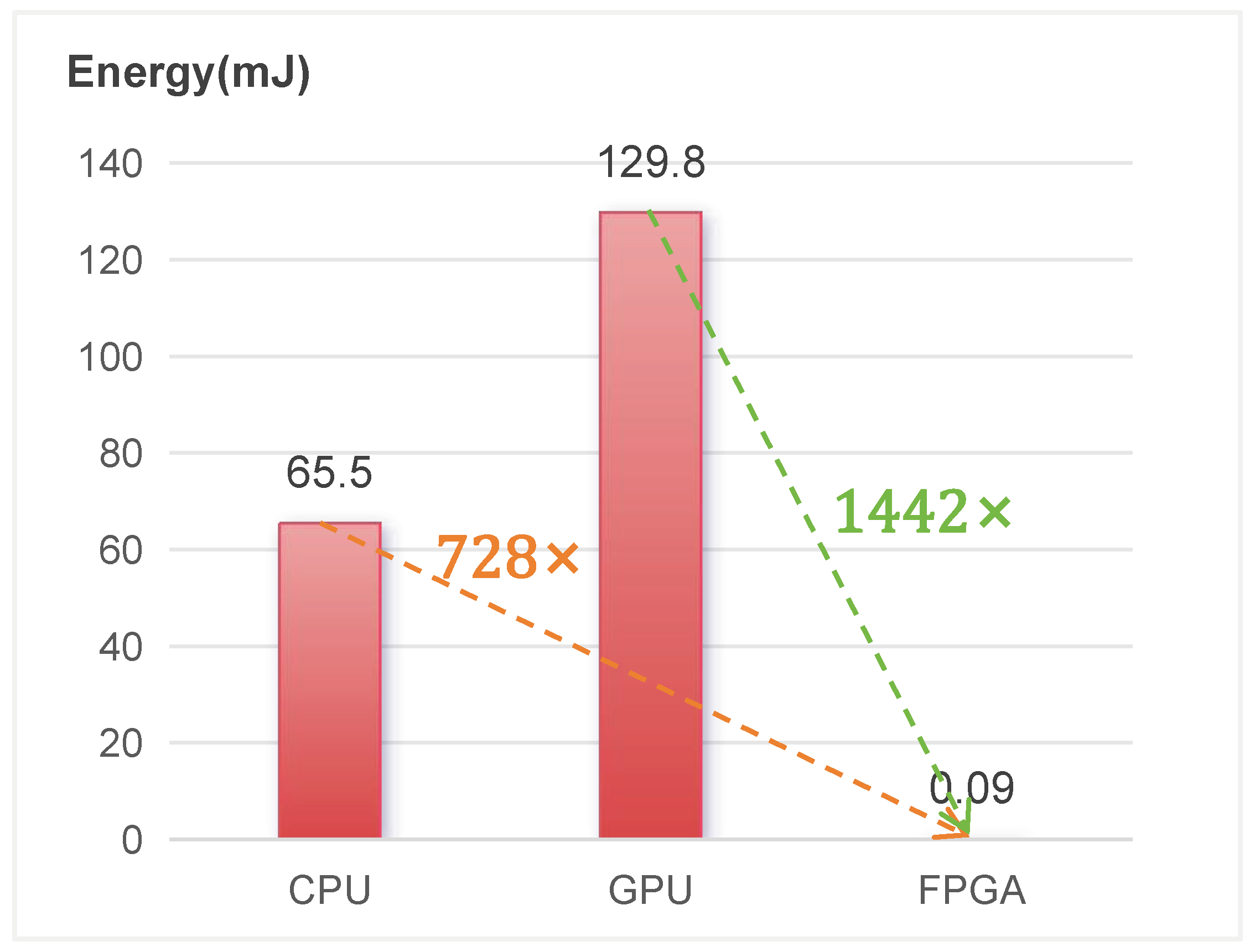
We conducted a comparative analysis between the proposed FPGA-based spiking LSTM accelerator and CPU, as well as GPU, evaluating latency and energy consumption for speech recognition inference. The inference latencies for CPU and GPU were recorded at 654.94 µs and 519.36 µs, respectively. Our FPGA-based spiking LSTM accelerator achieved a remarkable 8.3 × and 6.6 × speed enhancement over CPU and GPU, respectively, as depicted in Figure 12. Moreover, the energy consumed per inference in our Artix-7 XC7A200t-based system exhibited savings of 728 × and 1442 × compared with CPU and GPU, as illustrated in Figure 13.

4.3.2. Comparison with Traditional LSTM Accelerators Based on FPGA

To the best of our knowledge, there is currently no dedicated accelerator designed for spiking LSTM networks. Consequently, we conducted a comparative analysis between our spiking LSTM accelerator and existing accelerators tailored for traditional LSTM networks. The power-intensive matrix–vector multiplication operation inherent in traditional LSTM networks has been replaced by the addition of a spiking LSTM. As indicated in Table 3, the majority of traditional LSTM accelerators require thousands of multipliers or FPGA’s DSP. In contrast, our spiking LSTM accelerator does not require any DSP blocks, resulting in a substantial reduction in power consumption. Our accelerators showcase a power decrease by orders of magnitude when compared with other state-of-the-art accelerators for Automatic Speech Recognition applications. Additionally, our accelerators demonstrate superior energy efficiency in terms of the energy consumed per inference, which is as low as 66 µJ per inference.

5. Conclusions

In this paper, we present a spiking LSTM accelerator to accelerate the inference of the spiking LSTM network for Automatic Speech Recognition application. We implemented this accelerator on Xilinx Artix-7 XC7A200t and Zynq-7000 XC7Z020 FPGA, with a power consumption of 1.1 W and 0.84 W, respectively, when performing the inference for speech recognition with FSDD. The inference latency and accuracy are 78.93 µs and 72.88%, respectively. Its energy efficiency outperforms NVIDIA A100 GPU by 1442×. Additionally, compared with FPGA-based accelerators delicately designed for traditional LSTM networks, our spiking LSTM accelerator achieves a remarkable reduction in power consumption, amounting to orders of magnitude.

Author Contributions

Conceptualization, Y.Y. and T.Y.; methodology, T.Y. and F.D.; resources, Y.Y. and Z.W.; data curation, T.Y., F.D. and C.O.; writing—original draft preparation, T.Y. and Y.Y.; writing—review and editing, C.C. and Z.W. All authors have read and agreed to the published version of the manuscript.

Funding

This work has been supported by Guangdong Basic and Applied Basic Research Foundation (Grant No. 2023A1515012842, Grant No. 2020A1515110495).

Data Availability Statement

Data are contained within the article.

Conflicts of Interest

The authors declare no conflicts of interest.

Abbreviations

The following abbreviations are used in this manuscript:
ASRAutomatic Speech Recognition
LSTMLong Short-Term Memory
SNNSpiking Neural Network
RNNRecurrent Neural Networks
FPGAField Programmable Gate Array

References

  1. Yu, D.; Deng, L. Automatic Speech Recognition; Springer: Cham, Switzerland, 2015; Volume 1. [Google Scholar]
  2. Gondi, S.; Pratap, V. Performance and Efficiency Evaluation of ASR Inference on the Edge. Sustainability 2021, 13, 12392. [Google Scholar] [CrossRef]
  3. Hinton, G.; Deng, L.; Yu, D.; Dahl, G.E.; Mohamed, A.R.; Jaitly, N.; Senior, A.; Vanhoucke, V.; Nguyen, P.; Sainath, T.N.; et al. Deep Neural Networks for Acoustic Modeling in Speech Recognition: The Shared Views of Four Research Groups. IEEE Signal Process. Mag. 2012, 29, 82–97. [Google Scholar] [CrossRef]
  4. Pascanu, R.; Mikolov, T.; Bengio, Y. On the difficulty of training recurrent neural networks. Proc. Mach. Learn. Res. PMLR 2013, 28, 1310–1318. [Google Scholar]
  5. Sak, H.; Senior, A.W.; Beaufays, F. Long short-term memory recurrent neural network architectures for large scale acoustic modeling. In Proceedings of the INTERSPEECH, Singapore, 14–18 September 2014; pp. 338–342. [Google Scholar]
  6. Hochreiter, S.; Schmidhuber, J. Long Short-Term Memory. Neural Comput. 1997, 9, 1735–1780. [Google Scholar] [CrossRef] [PubMed]
  7. Cao, S.; Zhang, C.; Yao, Z.; Xiao, W.; Nie, L.; Zhan, D.; Liu, Y.; Wu, M.; Zhang, L. Efficient and effective sparse LSTM on FPGA with bank-balanced sparsity. In Proceedings of the 2019 ACM/SIGDA International Symposium on Field-Programmable Gate Arrays, Seaside, CA, USA, 24–26 February 2019; pp. 63–72. [Google Scholar]
  8. Han, S.; Kang, J.; Mao, H.; Hu, Y.; Li, X.; Li, Y.; Xie, D.; Luo, H.; Yao, S.; Wang, Y.; et al. Ese: Efficient speech recognition engine with sparse lstm on fpga. In Proceedings of the 2017 ACM/SIGDA International Symposium on Field-Programmable Gate Arrays, Monterey, CA, USA, 22–24 February 2017; pp. 75–84. [Google Scholar]
  9. Wang, M.; Wang, Z.; Lu, J.; Lin, J.; Wang, Z. E-LSTM: An Efficient Hardware Architecture for Long Short-Term Memory. IEEE J. Emerg. Sel. Top. Circuits Syst. 2019, 9, 280–291. [Google Scholar] [CrossRef]
  10. Wang, S.; Li, Z.; Ding, C.; Yuan, B.; Qiu, Q.; Wang, Y.; Liang, Y. C-LSTM: Enabling efficient LSTM using structured compression techniques on FPGAs. In Proceedings of the 2018 ACM/SIGDA International Symposium on Field-Programmable Gate Arrays, Monterey, CA, USA, 25–27 February 2018; pp. 11–20. [Google Scholar]
  11. Li, T.; Gu, S. FPGA Hardware Implementation of Efficient Long Short-Term Memory Network Based on Construction Vector Method. IEEE Access 2023, 11, 122357–122367. [Google Scholar] [CrossRef]
  12. Taherkhani, A.; Belatreche, A.; Li, Y.; Maguire, L.P. DL-ReSuMe: A Delay Learning-Based Remote Supervised Method for Spiking Neurons. IEEE Trans. Neural Netw. Learn. Syst. 2015, 26, 3137–3149. [Google Scholar] [CrossRef] [PubMed]
  13. Hazan, H.; Saunders, D.; Sanghavi, D.T.; Siegelmann, H.; Kozma, R. Unsupervised Learning with Self-Organizing Spiking Neural Networks. In Proceedings of the 2018 International Joint Conference on Neural Networks (IJCNN), Rio de Janeiro, Brazil, 8–13 July 2018; pp. 1–6. [Google Scholar] [CrossRef]
  14. Rathi, N.; Panda, P.; Roy, K. STDP-Based Pruning of Connections and Weight Quantization in Spiking Neural Networks for Energy-Efficient Recognition. IEEE Trans. Comput.-Aided Des. Integr. Circuits Syst. 2019, 38, 668–677. [Google Scholar] [CrossRef]
  15. Akopyan, F.; Sawada, J.; Cassidy, A.; Alvarez-Icaza, R.; Arthur, J.; Merolla, P.; Imam, N.; Nakamura, Y.; Datta, P.; Nam, G.J.; et al. TrueNorth: Design and Tool Flow of a 65 mW 1 Million Neuron Programmable Neurosynaptic Chip. IEEE Trans. Comput.-Aided Des. Integr. Circuits Syst. 2015, 34, 1537–1557. [Google Scholar] [CrossRef]
  16. Davies, M.; Srinivasa, N.; Lin, T.H.; Chinya, G.; Cao, Y.; Choday, S.H.; Dimou, G.; Joshi, P.; Imam, N.; Jain, S.; et al. Loihi: A Neuromorphic Manycore Processor with On-Chip Learning. IEEE Micro 2018, 38, 82–99. [Google Scholar] [CrossRef]
  17. Frenkel, C.; Lefebvre, M.; Legat, J.D.; Bol, D. A 0.086-mm2 12.7-pJ/SOP 64k-Synapse 256-Neuron Online-Learning Digital Spiking Neuromorphic Processor in 28-nm CMOS. IEEE Trans. Biomed. Circuits Syst. 2019, 13, 145–158. [Google Scholar] [CrossRef]
  18. Frenkel, C.; Legat, J.D.; Bol, D. MorphIC: A 65-nm 738k-Synapse/mm2 Quad-Core Binary-Weight Digital Neuromorphic Processor with Stochastic Spike-Driven Online Learning. IEEE Trans. Biomed. Circuits Syst. 2019, 13, 999–1010. [Google Scholar] [CrossRef] [PubMed]
  19. Pu, J.; Goh, W.L.; Nambiar, V.P.; Wong, M.M.; Do, A.T. A 5.28-mm2 4.5-pJ/SOP Energy-Efficient Spiking Neural Network Hardware with Reconfigurable High Processing Speed Neuron Core and Congestion-Aware Router. IEEE Trans. Circuits Syst. I Regul. Pap. 2021, 68, 5081–5094. [Google Scholar] [CrossRef]
  20. Li, S.; Zhang, Z.; Mao, R.; Xiao, J.; Chang, L.; Zhou, J. A Fast and Energy-Efficient SNN Processor with Adaptive Clock/Event-Driven Computation Scheme and Online Learning. IEEE Trans. Circuits Syst. I Regul. Pap. 2021, 68, 1543–1552. [Google Scholar] [CrossRef]
  21. Wang, B.; Zhou, J.; Wong, W.F.; Peh, L.S. Shenjing: A low power reconfigurable neuromorphic accelerator with partial-sum and spike networks-on-chip. In Proceedings of the 2020 Design, Automation & Test in Europe Conference & Exhibition (DATE), Grenoble, France, 9–13 March 2020; pp. 240–245. [Google Scholar] [CrossRef]
  22. Lotfi Rezaabad, A.; Vishwanath, S. Long short-term memory spiking networks and their applications. In Proceedings of the International Conference on Neuromorphic Systems, Oak Ridge, TN, USA, 28–30 July 2020; pp. 1–9. [Google Scholar]
  23. Shrestha, A.; Ahmed, K.; Wang, Y.; Widemann, D.P.; Moody, A.T.; Van Essen, B.C.; Qiu, Q. A spike-based long short-term memory on a neurosynaptic processor. In Proceedings of the 2017 IEEE/ACM International Conference on Computer-Aided Design (ICCAD), Irvine, CA, USA, 13–16 November 2017; pp. 631–637. [Google Scholar] [CrossRef]
  24. Rao, A.; Plank, P.; Wild, A.; Maass, W. A Long Short-Term Memory for AI Applications in Spike-based Neuromorphic Hardware. Nat. Mach. Intell. 2022, 4, 467–479. [Google Scholar] [CrossRef]
  25. Sengupta, A.; Ye, Y.; Wang, R.; Liu, C.; Roy, K. Going Deeper in Spiking Neural Networks: VGG and Residual Architectures. Front. Neurosci. 2019, 13, 95. [Google Scholar] [CrossRef]
  26. Jin, Y.; Zhang, W.; Li, P. Hybrid macro/micro level backpropagation for training deep spiking neural networks. In Proceedings of the 32nd International Conference on Neural Information Processing Systems, Red Hook, NY, USA, 3–8 December 2018; pp. 7005–7015. [Google Scholar]
  27. Roy, K.; Jaiswal, A.; Panda, P. Towards spike-based machine intelligence with neuromorphic computing. Nature 2019, 575, 607–617. [Google Scholar] [CrossRef] [PubMed]
  28. Kingma, D.P.; Ba, J. Adam: A Method for Stochastic Optimization. arXiv 2017, arXiv:1412.6980. [Google Scholar]
  29. Jackson, Z. Free Spoken Digit Dataset (fsdd). Technical Report. 2016. Available online: https://zenodo.org/records/1342401 (accessed on 10 February 2023).
  30. Horowitz, M. Computing’s energy problem (and what we can do about it). In Proceedings of the 2014 IEEE International Solid-State Circuits Conference Digest of Technical Papers (ISSCC), San Francisco, CA, USA, 9–13 February 2014; pp. 10–14. [Google Scholar] [CrossRef]
  31. torch.quantize_per_tensor. Available online: https://pytorch.org/docs/stable/generated/torch.quantize_per_tensor.html (accessed on 11 May 2023).
  32. Que, Z.; Nakahara, H.; Nurvitadhi, E.; Fan, H.; Zeng, C.; Meng, J.; Niu, X.; Luk, W. Optimizing Reconfigurable Recurrent Neural Networks. In Proceedings of the 2020 IEEE 28th Annual International Symposium on Field-Programmable Custom Computing Machines (FCCM), Fayetteville, AR, USA, 3–6 May 2020; pp. 10–18. [Google Scholar] [CrossRef]
  33. Mao, N.; Yang, H.; Huang, Z. An Instruction-Driven Batch-Based High-Performance Resource-Efficient LSTM Accelerator on FPGA. Electronics 2023, 12, 1731. [Google Scholar] [CrossRef]
Figure 1. Traditional LSTM cell.
Electronics 13 00827 g001
Figure 2. Spiking LSTM cell.
Electronics 13 00827 g002
Figure 3. Neuron in the spiking LSTM cell.
Electronics 13 00827 g003
Figure 4. Spiking encoding based on Poisson sampling for FSDD.
Electronics 13 00827 g004
Figure 5. Overall architecture of the spiking LSTM accelerator for automatic speech recognition.
Electronics 13 00827 g005
Figure 6. Low-cost circuit implementation of spiking LSTM gate.
Electronics 13 00827 g006
Figure 7. Timing diagram of the spiking LSTM layer.
Electronics 13 00827 g007
Figure 8. Implementation of spiking fully connected layer.
Electronics 13 00827 g008
Figure 9. Comparison of inference accuracy and memory footprint with int8, int16, and int32 quantizations.
Electronics 13 00827 g009
Figure 10. The weight storage method of the synaptic storage module: (a) Spiking LSTM layer.(b) Output layer.
Electronics 13 00827 g010
Figure 11. The algorithmic workflow for obtaining the inference model.
Electronics 13 00827 g011
Figure 12. The latency comparison using CPU, GPU, and the proposed accelerator.
Electronics 13 00827 g012
Figure 13. The energy comparison using CPU, GPU, and the proposed accelerator.
Electronics 13 00827 g013
Table 1. FPGA hardware resource utilization of the proposed spiking LSTM accelerator on Xilinx Artix-7 XC7A200t.
ResourceUtilizationAvailableUtilization%
LUT36,592133,80027.35
FF24,521269,2009.11
BRAM20236555.34
BUFG123237.50
Table 2. FPGA hardware resource utilization of the proposed spiking LSTM accelerator on Xilinx Zynq-7000 XC7Z020.
ResourceUtilizationAvailableUtilization%
LUT34,57853,20065.00
LUTRAM25617,4001.47
FF22,911106,40021.53
BRAM140140100.00
BUFG123237.50
Table 3. Comparison with other state-of-the-art FPGA-based accelerators.
ESE [8]C-LSTM [10]E-LSTM [9][32][33][11]OursOurs
Year201720182019202020232023--
PlatformXCKU060Virtex-7Arria10GX2800Alevo U50ZCU102XC7A200tXC7Z020
LUT293,920621,201--122,935187,08436,59234,578
FF453,068234,562--407,690290,30424,52122,911
BRAM947942--282610202140
LUTRAM69,9390--553600256
DSP15042347-43684224145700
ArchitectureGoogle LSTMSmall LSTMVanilla LSTM-Google LSTM1024-102442-200-1042-200-10
DatasetTIMITTIMITTIMITUCF101-TIMITFSDDFSDD
Accuracy79.30%75.43%-70.10%--72.88%72.88%
Quant.int12int16int8int8int16int12int16int16
Freq. (MHz)200200200260280200120120
Latency (µs)575.423.933978612.478.9378.93
Power (W)412215.912532.3151.10.84
Energy/Inf. (µJ/I)23371193804125316,0881868766
Disclaimer/Publisher’s Note: The statements, opinions and data contained in all publications are solely those of the individual author(s) and contributor(s) and not of MDPI and/or the editor(s). MDPI and/or the editor(s) disclaim responsibility for any injury to people or property resulting from any ideas, methods, instructions or products referred to in the content.