Article

Fault Ride-Through Method for Interline Power Flow Controller Based on DC Current Limiter

1
School of Electrical Engineering, Sichuan University, Chengdu 610065, China
2
Power Internet of Things Key Laboratory of Sichuan Province, Chengdu 610072, China
3
State Grid Sichuan Electric Power Research Institute, Chengdu 610041, China
4
School of Public Administration, University of Electronic Science and Technology of China, Chengdu 611731, China
*
Author to whom correspondence should be addressed.
Electronics 2024, 13(6), 1038; https://doi.org/10.3390/electronics13061038
Submission received: 16 January 2024 / Revised: 5 March 2024 / Accepted: 6 March 2024 / Published: 11 March 2024

Abstract

:
The interline power flow controller (IPFC) based on a modular multilevel converter with a half-bridge configuration can control the active and reactive power flows of multiple alternating current (AC) lines. However, it forms a multiterminal system on the direct current (DC) side, which leads to DC faults. To reduce the protection and clearance requirements on the DC side of IPFCs, this paper proposes a hybrid current limiter topology suitable for generating a DC-side fault ride-through scheme. The current limiter employs a low-loss branch in steady-state conditions; when the fault occurs, a commutation capacitor and controllable power electronic devices are used to transfer the fault current to the current-limiting branch. To clarify the operating principles of the current limiter, the working states of each stage and electrical stress of each device are analyzed. Different components with varying limiter parameters are also discussed, and optimal parameters to achieve the best limitation effect are discussed. PSCAD simulations show that the proposed limiter can limit the overcurrent effectively, and DC-side fault clearance can be achieved easily with this fault ride-through strategy.

1. Introduction

In recent years, there has been a continuous increase in power demand, leading to a significant mismatch between the power transmission capacity of power lines and the inability of the current grid systems to meet the power demand. To address this issue, a flexible AC transmission system (FACTS) has been proposed previously. The use of power electronics and corresponding control technologies enables flexible and rapid adjustment of the impedance, voltage, and phase of AC systems, which in turn facilitates flexible control of the active and reactive power flows in lines, thus meeting the needs of power grids during operation [1]. Some scholars have also proposed adding Unified Power Quality Conditioners (UPQCs) to transmission lines to solve power quality problems for sensitive load under weak grid conditions and isolated areas or islands connected to the mainland through long submarine cables [2,3].
One of the most typical FACTSs is the unified power flow controller; however, it can only control the active and reactive power in AC lines. With the increasing amount of renewable energy, power fluctuations have become more common. Due to this, power lines suffer from overload, and this is becoming a common problem that needs to be addressed urgently. Thus, more AC lines must be controlled, and an interline power flow controller (IPFC) was proposed.
The IPFC is a new generation of FACTS that possesses powerful power flow control ability [4]. It can quickly and flexibly control the active and reactive power flows of multiple lines, thereby significantly improving the transmission efficiency [5,6,7]. Unlike series or parallel FACTS, the IPFC can have multiple converter stations, each connected by a DC bus. When a fault occurs in the DC bus, the DC current rapidly increases. If the fault current is not limited, it will cause the fault current to be too large, ultimately leading to the IPFC exiting operation.
Specifically, the converter stations of the IPFC are in series with the AC line, whereas they are connected by DC lines on the DC side; this forms a multiterminal system. Therefore, the IPFC suffers from DC faults, analogous to DC grids. It is known that due to the low inertia and low impedance characteristics of DC grids, the DC fault current and its amplitude generally increase sharply during the short-circuit fault period [8,9]. Because DC system fault currents are characterized by fast rising rates, high amplitudes, and no zero-crossing points, they are more challenging to cut off than AC fault currents. Without considering the AC-measured feed-in current, after a short-circuit fault occurs on the DC side of the modular multilevel converter (MMC), the MMC submodule can be equated to a second-order RLC circuit with a rapid increase in the capacitor discharge current and simultaneous large voltage drop. When a DC short-circuit fault causes the bridge arm current or capacitor voltage to exceed the protection threshold, the system enters a blocking state after a short delay, and the IPFC exits the operation. Here, we designed a fault current limiter (FCL) for the DC side of the IPFC. The current limiter is connected in series in the DC line of the IPFC and presents a low-impedance characteristic during normal operation and high-impedance characteristic during a fault on the DC side to limit the fault current rise [10].
Several researchers have conducted extensive studies on current-limiting devices for DC systems. Several strategies have been proposed to solve the DC fault clearance problem. Typically, a DC circuit breaker (DCCB) is used to cut off the faulty line [11]. However, owing to problems with arc extinguishing and insulation technology [12], the increase in maintenance costs caused by the duplication of the interrupting current [13], and increasing metal oxide arrester energy consumption [14,15], it becomes too expensive to solely rely on DCCB to isolate the faulty line of the power grid. Reference [16] proposed a hybrid circuit breaker without load current switching that can reduce the conduction loss during normal operation; however, the rate of fault current rise is significantly fast. Therefore, it is necessary to implement appropriate measures to limit the increase in the fault current before the DCCB operates.
Some scholars have proposed installing smoothing reactors at both ends of the DC line to limit the rate of current increase after a fault. However, the installation of such reactors increases project costs and results in damping characteristics and reduced system stability [17,18]. Therefore, it is crucial to select a suitable fault current limiter for the DC system of an IPFC.
Currently, DC fault current limiters can be categorized into two main groups: superconducting fault current limiters (SFCLs) [19,20,21] and current limiters based on power limiters [22,23]. SFCLs utilize superconducting materials to enhance the line impedance via the quench phenomenon that occurs during a fault to limit the fault current. In [24], a quenching method was proposed for a balanced SFCL using a neutral line to increase the current-limiting rate. However, owing to the difficulty in producing superconducting materials and the high maintenance costs, there are currently few applications in high-voltage DC systems. Power electronics-based current limiters can be further categorized into solid-state fault current limiters (SSFCLs) and hybrid current limiters. SSFCLs have the advantages of a short action time, no arc, no light, and no sound, but they also have the disadvantages of high cost and device loss. Hybrid current limiter combines the advantages of power electronic devices and mechanical switches. References [25,26] present two current limiter topologies for voltage-sourced converter-based high-voltage (VSC-HVDC) faults with parameter design methods and reclosing schemes.
At present, most of the fault current limiter topologies proposed by scholars are aimed at flexible DC power grids, and there is currently no fault current limiter proposed for FACTS equipment, especially the IPFC. The modular multilevel converter-based interline power flow controller (MMC-IPFC) and VSC-HVDC have similar DC structures. When the DC bus is faulty, the discharge mechanism of the MMC submodule is the same. But their operating characteristics are fundamentally different. Existing fault limiters are problematic when used directly in the IPFC. Firstly, the IPFC operates with a bidirectional DC current, so the current limiter needs to have strong bidirectional current capability. In addition, if the fault current reaches the MMC blocking value after the fault, it will cause the IPFC to exit operation. After the IPFC exits, the reactive power of the auxiliary control side of the IPFC will not be controlled, and at the same time, the reactive power and active power of the main control side IPFC will lose control. The existing inductive current limiters still have the limiting inductance connected in series in the circuit when the circuit breaker is activated. This will increase the breaking time of the circuit breaker and the energy consumption of the lightning arrester in the circuit breaker.
Therefore, it is necessary to develop a new type of fault current limiter that is more cost-effective and practical for the IPFC. To solve these problems, this study proposes an FCL topology suitable for DC-side fault ride-through of IPFCs. The novelty of the proposed strategy is as follows.
  • A DC-side fault current limitation method for the IPFC is proposed for the first time, which can assist with the DC-side fault ride-through of the IPFC and effectively limit the fault current.
  • The proposed current limiter can limit the fault current below the MMC blocking current and enable IPFC non-blocking fault ride-through, thereby improving the survival capability of the IPFC. After the circuit breaker cuts off the fault, the IPFC can resume normal operation in a short period of time.
  • The proposed IPFC limiter exhibits low-impedance characteristics in the steady state and low on-state loss, ensuring that the normal operation of the IPFC is not affected.
  • The proposed current limiter only requires the use of thyristors without the need for expensive fully controlled devices. At the same time, the fault current is limited to a lower level, which can greatly reduce the energy consumption of the lightning arrester in the DC circuit breaker. This will reduce the overall cost.
The remainder of this paper is organized as follows. In Section 2, we present the topology of the proposed current limiter followed by an analysis of its action processes of the current limiter in stages. In Section 3, we examine the influence of the device parameters on the current-limiting effect and provide a parameter selection method. Section 4 presents the pre-charge capacitor charging scheme and fast bypass of the current-limiting inductor. In Section 5, the proposed current limiter is validated in a DC and three-terminal IPFC system and compared with other current-limiting schemes. Finally, Section 6 concludes the paper.

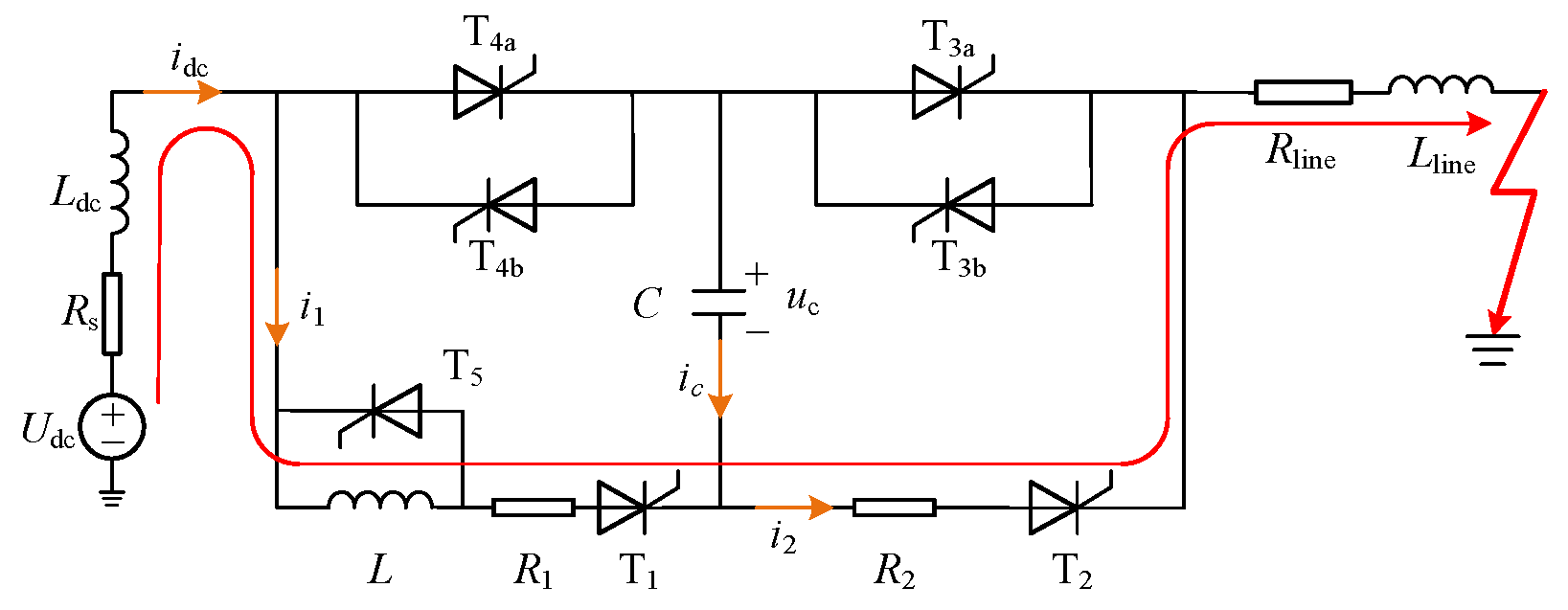
2. Current Limiter Topology and Current-Limiting Process Suitable for IPFC DC Side

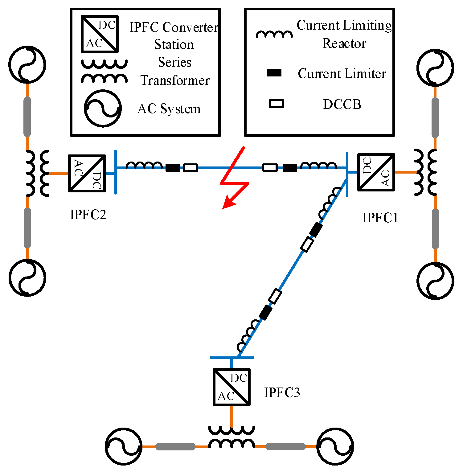
2.1. Topology of IPFC

Figure 1 illustrates a two-terminal IPFC system with converter stations connected by series transformers at each terminal of the DC side. The IPFC has at least one auxiliary control side, whose main function is to maintain the DC-side voltage, and at the same time can control the reactive power flow of the line. The IPFC can have multiple master control sides, with an injection voltage Use superimposed on the voltage source by the voltage generated by the inverter at the converter station. As a result, the IPFC can control the active and reactive power flow of multiple lines on the master control sides.

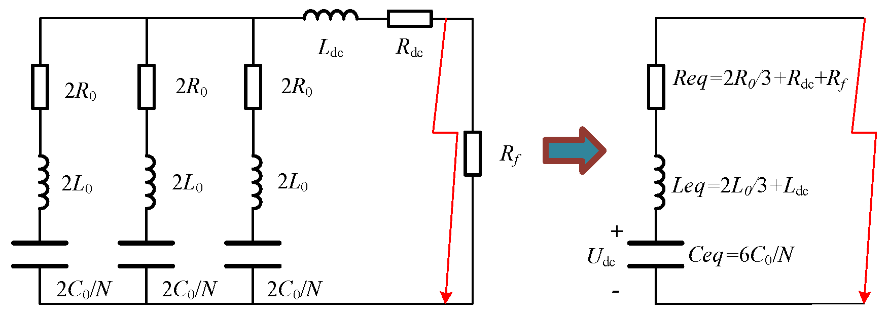
2.2. DC Fault Vulnerability Analysis

The equivalent circuit diagram of the submodule discharge before blocking the MMC-IPFC converter station after a fault is shown in Figure 2. R0 and L0 denote the equivalent resistance and equivalent inductance in a single bridge arm, respectively; C0 is the capacitance value of a single MMC submodule; and N denotes the number of the submodules in the input state. Rdc and Ldc are the equivalent inductance and resistance of the converter up to the fault point, respectively, and Rf is the fault resistance. As the three-phase units of the MMC are identical and connected in parallel, they can be simplified to an RLC second-order equivalent circuit. The figure shows that due to the small impedance in the circuit after the fault, the fault current rises and the DC voltage drops quickly.

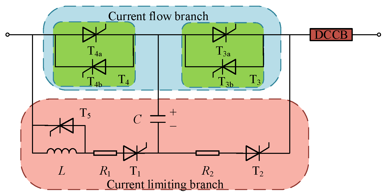
2.3. IPFC Fault Current Limiter Topology

Figure 3 shows the proposed DC fault-current limiter and its connection to the DC circuit breaker. The limiter comprises two main components: the flow branch under normal conditions and the limiter branch. To accommodate the positive and negative currents that occur during the normal operation of the IPFC, the flow branch adopts a structure of two thyristors connected in reverse parallel. The limiter branch comprises three parts: (1) the pre-charge capacitor C, which commutates the fault current to current-limiting path and ensures the reliable shutdown of T3 by pre-charging its voltage; (2) the auxiliary commutation branch comprising auxiliary commutation resistance R2 and thyristor T2, which transfers current from the flow branch to the current-limiting branch and limits the current increase; and (3) the main current-limiting inductor L, current-limiting resistor R1, and thyristors T1 and T5. Inductors L and R1 further suppress the fault current, whereas T5 bypasses inductor L quickly when the circuit breaker operates to reduce the energy consumption of the arrester and the associated costs.

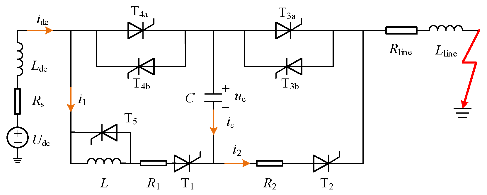
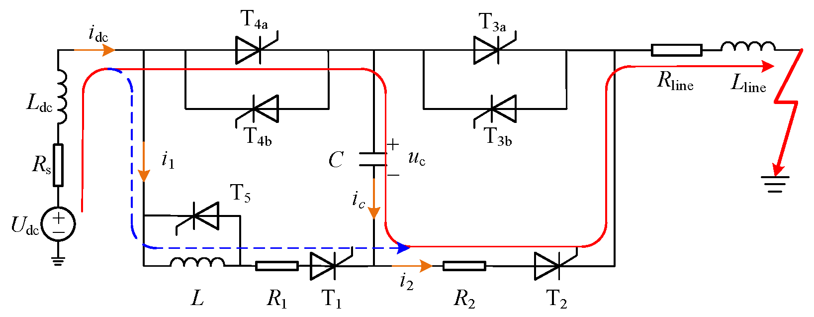
2.4. Action Process and Theoretical Analysis of Current Limiter

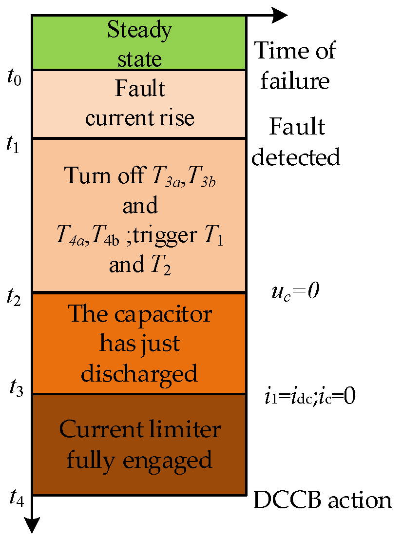
2.4.1. Current Limiter Action Process

The current limiter was positioned at the outlet of the converter. Assuming that the current flows from left to right, the limiter carries both positive and negative currents during normal operation. In the event of a DC-line fault, the converter station supplies power to the current limiter. When the fault current flows from right to left, it increases rapidly. However, when the fault current flows from left to right, it rapidly decreases to zero and then increases again in the positive direction.
  • During normal operation, the thyristors T3 and T4 are in a normal trigger state, and the current flows through the current branch as usual.
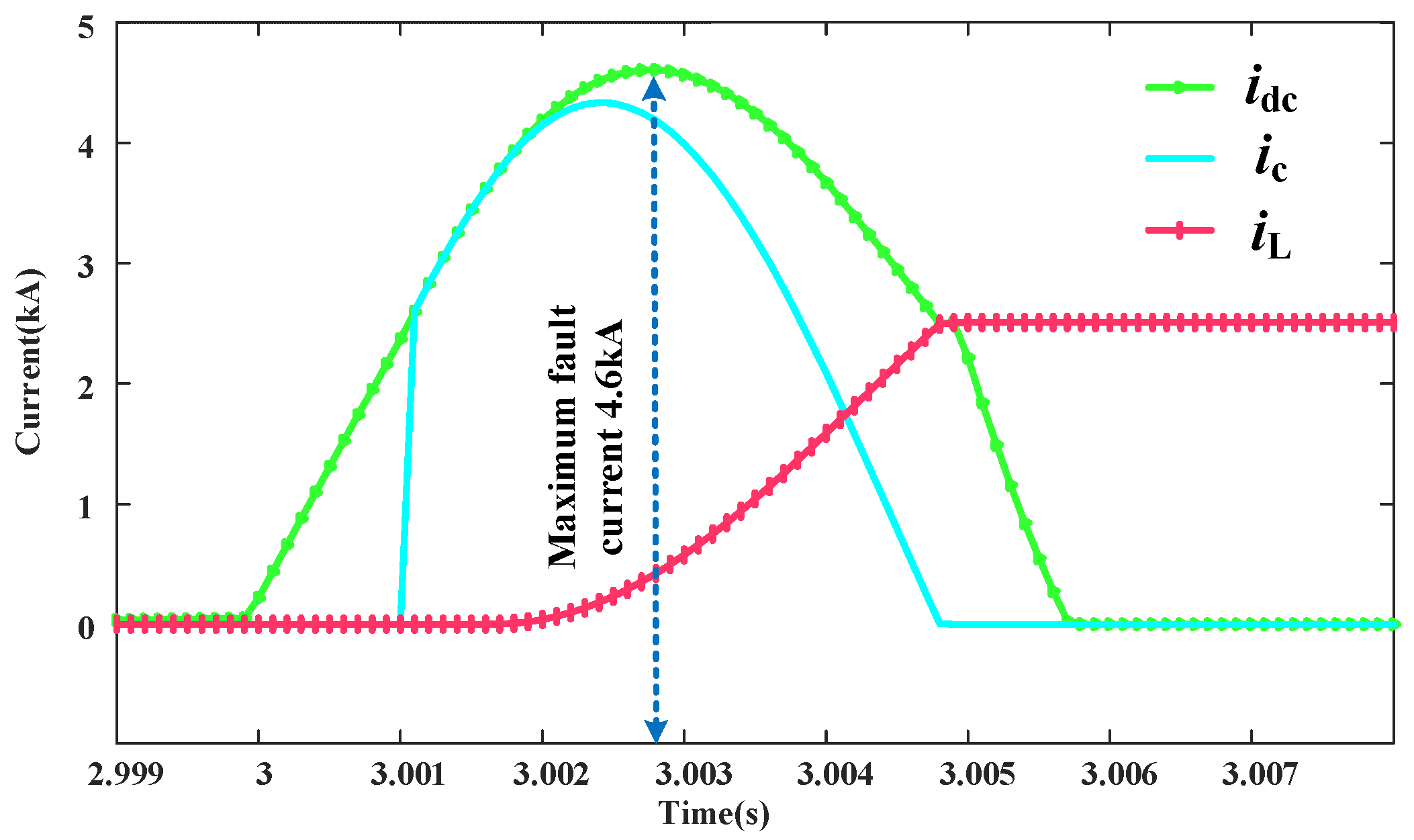
  • When a fault occurs, the current rapidly increases. When the current reaches the fault detection condition, T3 and T4 are turned off, and T2 and T1 are turned on. Thyristor T2 conducts under the forward voltage of the capacitor C, and the current is quickly transferred to the auxiliary commutation branch. After the current of thyristor T3a decreases to zero, capacitor C is not discharged completely, and T3a withstands the reverse voltage of capacitor C for a reliable shutdown.
  • As the voltage of capacitor C drops to zero, the current continues to charge it and thyristor T1 turns on due to the forward voltage, putting the main current-limiting branch into operation. As the current increases, when the sum of the capacitor voltage and resistor R1 voltage exceeds the system voltage, the line current begins to decrease. After T4a current drops to zero, the thyristor is turned off; the voltage across C reaches its maximum value, and the fault current is transferred to the current-limiting branch.

2.4.2. Theoretical Analysis of Current-Limiting Process

Assuming a unipolar ground fault, as shown in Figure 4, occurs on the DC line at time t0, where Ldc represents the current-limiting reactor, RS is the system resistance, and Rline and Lline represent the line impedances as lumped parameters. In this case, the capacitor of the MMC submodule is not considered to be discharged; instead, it is replaced by a DC power supply Udc. At the end of this section, we will present the simulation results applied to IPFC.
(1)
t0t1 fault detection stage
During normal operation, the current passes through the flow branch, resulting in minimal loss of the current limiter. However, in the event of a fault, the current increases sharply and continues to flow through the current branch until reaching the DC grid protection and detection device. Figure 5 illustrates the current path during this stage.
The representation of the dynamic process of the system is as follows:
i dc = U dc R s + R line + ( I n U dc R s + R line ) e ( t t 0 ) / τ 1
where In is the DC current during normal operation and τ1 is the time constant.
τ 1 = L dc + L line R s + R line
(2)
t1t2 current transfer stage
At time t1, the DC current reaches the fault detection condition, triggering T1 and T2 and signaling T3a and T3b to shut down. Owing to the pre-charged capacitor voltage, T2 can bear the forward voltage and commutate the fault current from the current branch to the auxiliary commutation branch. Further, the pre-charged capacitor voltage is added to both ends of T3a, causing the voltage at both ends to reverse and rapidly decrease the anode current. Additionally, the preset voltage of capacitor C is opposite to the line voltage, which aids in reducing the current on the line and absorbing it to the branch where C is located. After the current decreases to zero, the capacitor remains partially charged, and the voltage at both ends is added to the T3a thyristors to ensure a reliable turn-off. To guarantee a reliable thyristor turn-off, the capacitor discharge time should exceed 100 μs. The current path during this stage is shown in Figure 6.
The dynamic description of the process is:
{ U dc = ( R s + R 1 + R line ) i dc + ( L dc + L line ) d i dc d t + u c i dc = C d u c d t
The initial pre-charge value of capacitor C is U0; ignoring the time at which the current in T3a drops to zero, it is approximately considered that the current is immediately transferred to the T2 branch at t1, and T3a is immediately turned off. Let the operating current of the current limiter at time t1 be idc(t1) = ic(t1) = I0. Substituting this into (3), the following can be obtained:
{ U c = U dc + B 1 2 + B 2 2 sin ( ω d ( t t 1 ) + φ 1 ) e α ( t t 1 ) i dc = C ( α 2 + ω d 2 ) ( B 1 2 + B 2 2 ) sin ( ω d ( t t 1 ) + φ 1 + φ 2 ) e α ( t t 1 )
In the formula:
α = R line + R s + R 2 2 ( L dc + L line )
ω d = 1 C ( L dc + L line ) ( R line + R s + R 2 ) 2 4 ( L dc + L line ) 2
B 1 = U dc U 0
B 2 = 1 ω d C I 0 + α ω d B 1
φ 1 = arctan B 1 B 2
φ 2 = arctan ω d α
(3)
t2t3 capacitor commutation stage
At time t2, the discharge of capacitor C is completed and the voltage across it drops to zero. As the system continues to charge the capacitor, its voltage begins to increase. At this point, the T1 thyristor is triggered by the forward voltage, and the current begins to transfer to the main current-limiting branch. Figure 7 illustrates the current path during this process.
At this point, as the current flowing through the T4a thyristors decreases to zero, the fault current is completely transferred to the current-limiting branch, and the current limiter is fully activated on the DC line. Because the voltage at both ends of the capacitor at this point is higher than the system voltage, T4a bears the reverse voltage after current switching to ensure reliable thyristor shutdown. A dynamic description of this process can be obtained by applying Kirchhoff’s voltage law (KVL) as follows:
{ U dc = L dc d i dc d t + R 2 i dc + u c i dc = i 1 + i c i c = C d u c d t u c = L d i 1 d t + R 1 i 1
As capacitor C charges, its voltage uc gradually increases. When the sum of uc and the line resistance voltage exceeds the system voltage Udc, the line current begins to decrease. At this point, the voltage across the current-limiting reactor on the line becomes negative on the left and positive on the right. The capacitor continues to charge until the commutation process ends at time t3, when its voltage exceeds the system voltage.
(4)
t3t4 main current-limiting stage
At time t3, the capacitive current ic drops to zero, and the current is completely transferred to the current-limiting branch, fully switching on the current limiter and entering the main current-limiting stage. The current path for this stage is shown in Figure 8.
The dynamic process of the system at this stage can be expressed as:
i dc = U dc R sum + ( I 2 U dc R sum ) e ( t t 3 ) / τ 2
τ 2 = L sum R sun
where Rsum = Rs + R1 + R2 + Rline and Lsum = Ldc + L + Lline. The calculation method for I2 = idc(t3) is as follows. By substituting uc(t2) = 0 into (4), we can obtain the starting time t2 of the capacitor commutation and line current idc(t2) = I1 at that time. Therefore, the initial condition for (11) is given by (14). By substituting (14) and the condition that the capacitive current ic(t3) = 0 into (11) at time t3, we obtain I2.
{ u c = 0 i 1 = 0 i dc = I 1
To further analyze the reliable turn-off of T4a, we need to consider the voltage at both ends of capacitor C at time t2+t3−. At this time, the voltage is equal to the voltage at both ends of the branch where T1 is located. At time t3, the current in T4a drops to zero and the voltage across the capacitor reaches its maximum value. At time t3+, T4a turns off the capacitive commutation and the process ends. Assuming a negligible line resistance and impedance, we can apply KVL to obtain
{ u T 3 a ( t 3 + t t 4 ) = L d i dc d t + R 1 i dc u c _ max U dc = L d i dc d t + L dc d i dc d t + R 1 i dc + R 2 i dc
From (15), we can obtain:
u T 3 a ( t 3 + t t 4 ) = ( U dc L dc d i dc d t R 2 i dc ) u c _ max
Equation (16) indicates that based on the previous analysis, uc_max is larger than Udc. Therefore, it can be inferred that uT3a(t3+ < t < t4) < 0, which implies that the T3a thyristors will immediately bear the reverse voltage after the capacitive commutation is completed. They can be turned off reliably after withstanding the reverse voltage for a certain period.
The various time nodes of the current-limiting process are shown in Table 1. Figure 9 shows the control strategies for each stage during the operation of the current limiter.

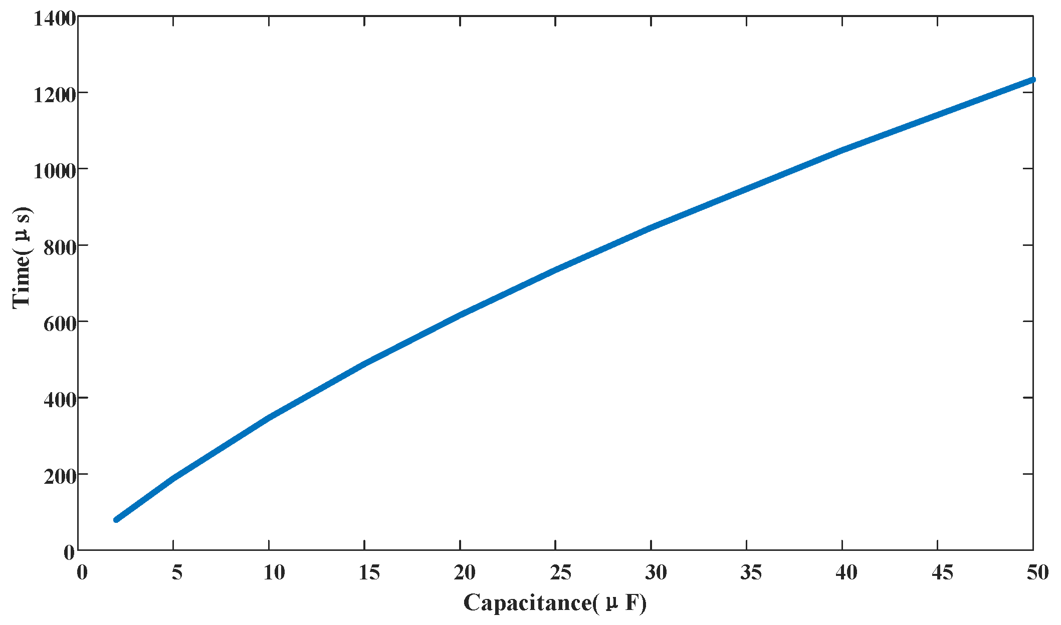
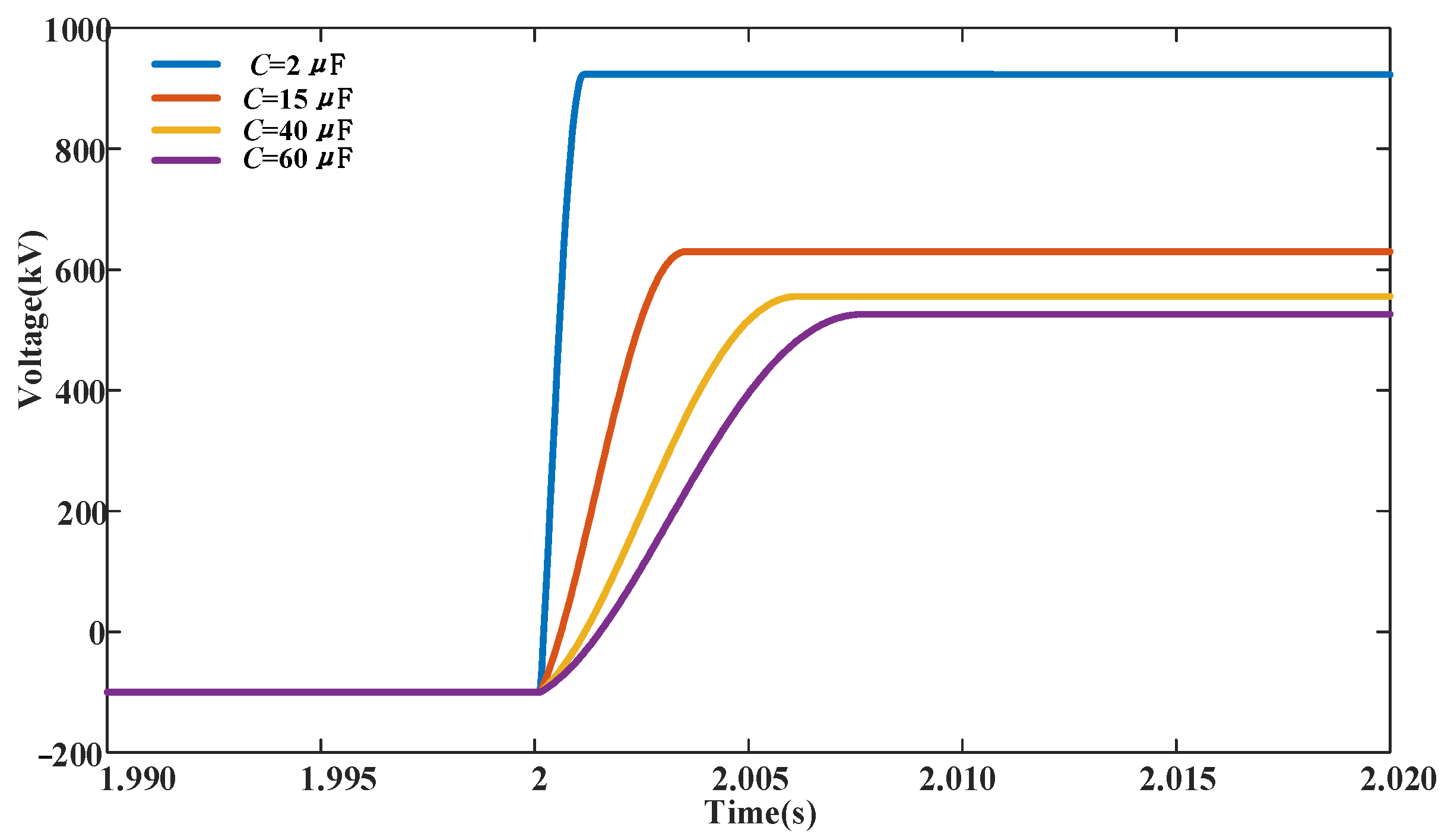
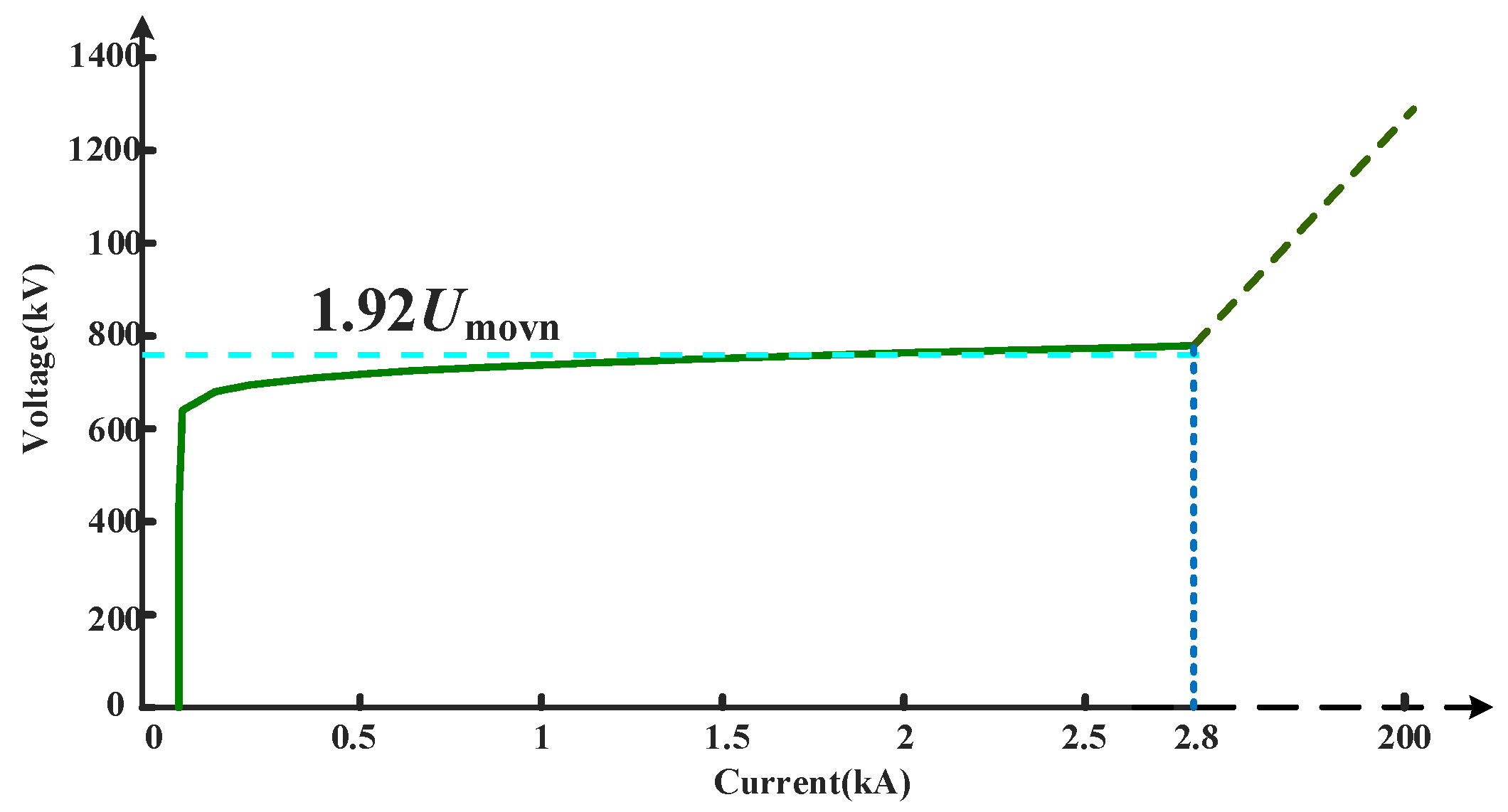
3. Parameter Design of Current Limiter

For the t1–t2 current transfer stage, it is necessary to ensure that the current is commutated to the auxiliary commutation branch. After the commutation is completed, the thyristor must be reliably turned off; that is, T4a must withstand the reverse voltage for a certain period of time.
We first consider that the current can be transferred to the auxiliary commutation branch, assuming that the DC line is a 400-kV system with a rated current of In = 2 kA. The system detects that the fault occurs when the DC current is 20% higher than the system rated value, and idc(t1) = 2.4 kA. To ensure successful commutation, the pre-charge capacitor voltage must satisfy (17):
U 0 i dc ( t 1 ) R 2 > 0
In this study, the pre-charging voltage was set to 100 kV. It can be observed from (17) that when R2 is significantly large, the commutation fails as shown in Figure 10. From Figure 10, we can see that as the resistance R2 increases, the amplitude of the fault current decreases. But when the resistance value increases to a certain extent, the current limiter will fail to perform commutation and lose its current-limiting ability. Therefore, the resistance value of R2 should be less than the value that causes the current limiter to fail commutation. Considering that the function of R2 is to convert the fault current into the limiting current, rather than limit the rise of the fault current, the selected resistance value of R2 does not need to be very large. Therefore, on the basis of considering a certain design margin, economy, and current-limiting effect, we selected a resistor R2 with 20 Ω as the resistance value of the auxiliary commutation resistance.
Figure 11 shows the relationship between the size of the pre-charge capacitor and the time used in the current switching stage, where Δt1 = t2t1; it can be seen that Δt1, that is, the time for discharging the capacitor, will increase with the increase in capacitance. A capacitor of tens of μF can ensure that the discharge time is more than 100 μs and thyristor T3a is turned off.
The selection of the capacitors should also take into account the system characteristics of the t2t3 capacitor commutation stage. We first consider the influence of capacitance on the capacitance commutation time Δt2 = t3t2 and the idc_max of the maximum current in the commutation process. The smaller the capacitance, the faster the charging speed of the line to the capacitor, and the faster the capacitor voltage rises, which will accelerate the current increase on the T1 branch at this stage, which is conducive to the completion of capacitor commutation; at the same time, it will also reduce idc to decrease the value of idc_max. The relationship between the value of C and Δt2 and idc_max is shown in Figure 12, and the results are consistent with the above inference.
However, considering the capacitor voltage after the capacitor is charged, it is easy to know from the analysis that the smaller the capacitor, the more obvious the charging effect, and the higher the voltage across the capacitor after commutation is completed. Figure 13 shows the voltage change for different capacitance values during the current-limiting process, which proves the correctness of the above inference.
For the parameter selection of commutation capacitor C, the first consideration should be to ensure the reliable shutdown of the thyristor T3a. Otherwise, the fault current will still flow through the current branch, and the current limiter will lose its current-limiting ability. From Figure 11, it can be seen that Δt1 increases with the increase in capacitance value. On the basis of considering twice the threshold, capacitance exceeding 5 μF can ensure reliable turnoff of the thyristor. In addition, commutation capacitors can also affect the fault current and the magnitude of Δt2. From Figure 12, it can be seen that as the capacitance value increases, the values of Δt2 and idc_max will both increase. To ensure that MMC does not lock during fault, idc_max should be limited to below 6 kA. Figure 13 also shows the variation in commutation capacitor voltage with the change in capacitance value. A too-small capacitance value can cause the capacitance voltage to be too high, causing more insulation problems for the components. Considering the above reasons, the commutation capacitance was taken as 20 μF.

4. Pre-Charge Capacitor Charging Scheme and Current-Limiting Inductor Fast Bypass Technology

4.1. Pre-Charging Capacitor Charging Scheme

Currently, for high-voltage capacitor charging in DC systems, external DC/DC converters and laser energy delivery are generally used. These systems require additional large investments, and at the same time, cause significant security and control problems. In this study, a topological structure was added to charge the capacitors. The charging method is illustrated in Figure 14, where Tchar is the switch of the pre-charging circuit; Cchar is the variable capacitor, whose purpose is to control the pre-charging voltage of the commutation capacitor; and the R1 resistor in the charging circuit can limit the charging current. This method utilizes the existing system structure to charge the commutation capacitor, and can monitor the voltage of the capacitor while the system is running to ensure that the voltage is maintained at a normal level.

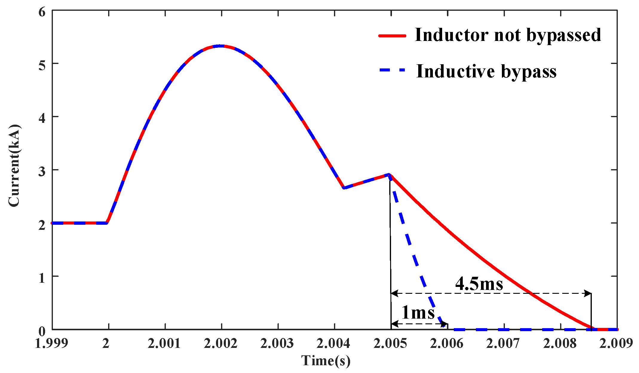
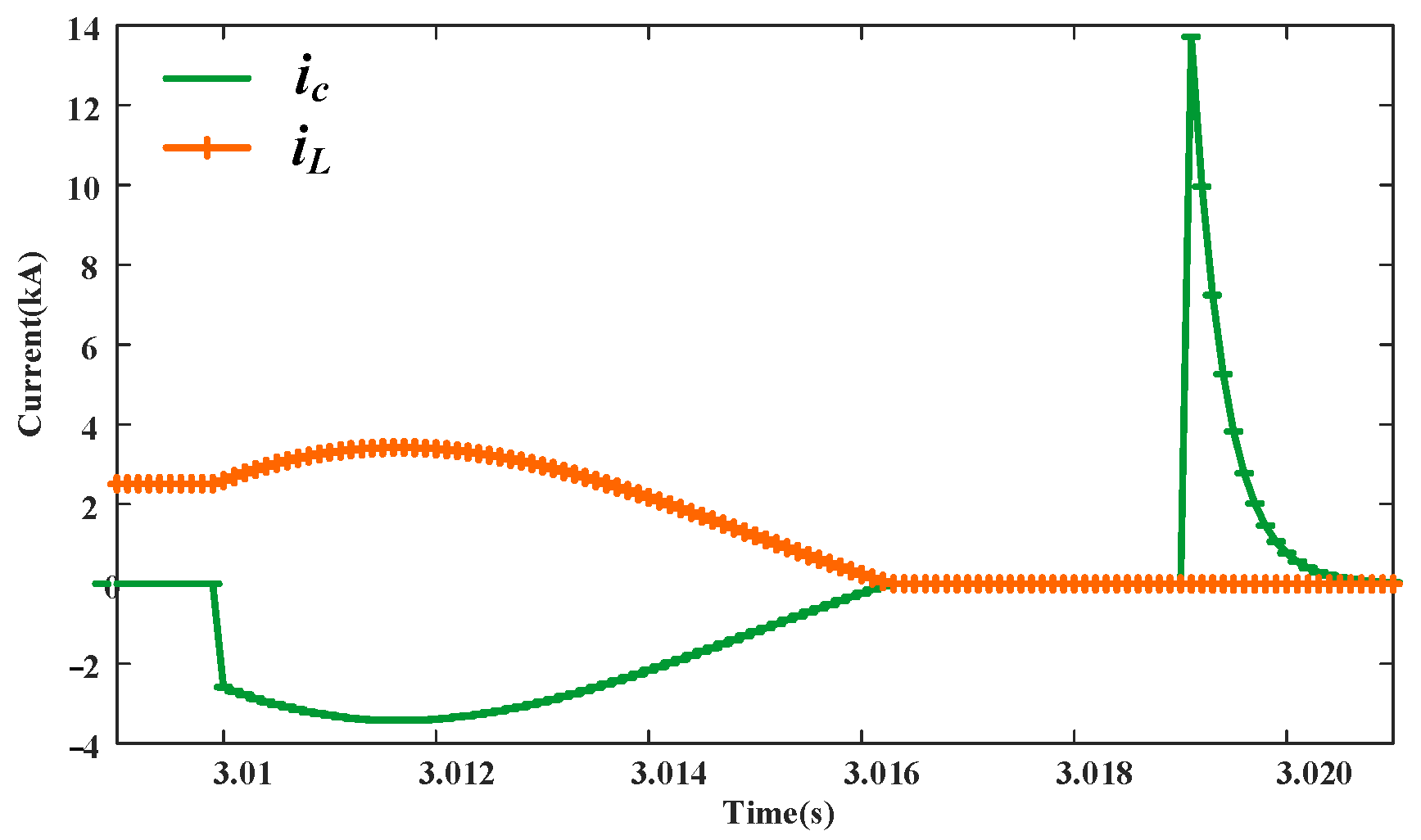
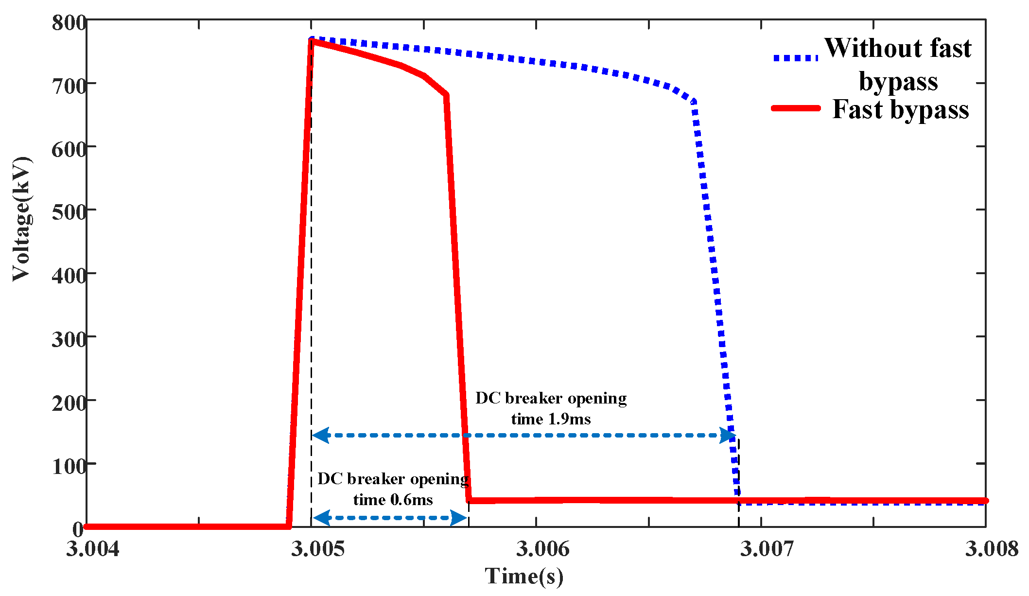
4.2. Current-Limiting Inductor Fast Bypass Technology

4.2.1. Inductive Fast Bypass Method

The DC current limiter curbs the escalation of the fault current following a fault and provides a window for fault detection. Once a faulty line is identified, the DC circuit breaker on the line can interrupt the fault current.
Considering the ABB hybrid DCCB as an example, the arrester kicks in and consumes energy immediately after the operation of the main circuit breaker, causing the line fault current to drop instantaneously. However, in the current limiter scheme outlined in this paper, the main current-limiting inductance L remains connected in series with the faulty circuit even after the circuit breaker is tripped, thereby hindering the attenuation of the fault current. To address this issue, this paper proposes the use of current-limiting inductance fast-bypass technology, which bypasses the current-limiting inductance L once the circuit breaker operates, effectively removing it from a faulty circuit. This reduced the cutoff time of the circuit breaker and the energy absorbed by the arrester. After the fault is cleared, the pre-charged capacitor is activated, forming an energy transfer loop that eventually dissipates the energy stored in the inductor. The specific process is described below.
(1)
Once the system experiences failure, the current limiter is activated in the fault circuit using the sequence of actions outlined in the previous section. This is repeated until the capacitor commutation current limiter was completely operational. Further refinement of the system may be required to ensure optimal performance in the event of future failure.
(2)
Fast bypass of current-limiting inductor.
When a fault is detected by the system protection mechanism, the IGBT in the DCCB transfer branch is deactivated, causing the arrester to begin consuming energy, resulting in a rapid decrease in the fault current. At this point, the voltage across the current-limiting inductor suddenly becomes negative on the left and positive on the right. When T5 is triggered, the inductance L is bypassed and the current in L remains constant while the energy is temporarily stored in the loop. Because of the arrester, the fault circuit current continues to decrease until it reaches the operational value of the isolation switch, at which point the switch is triggered and the fault is fully removed from the line. Further system improvements may be required to optimize the performance in the event of future faults.
(3)
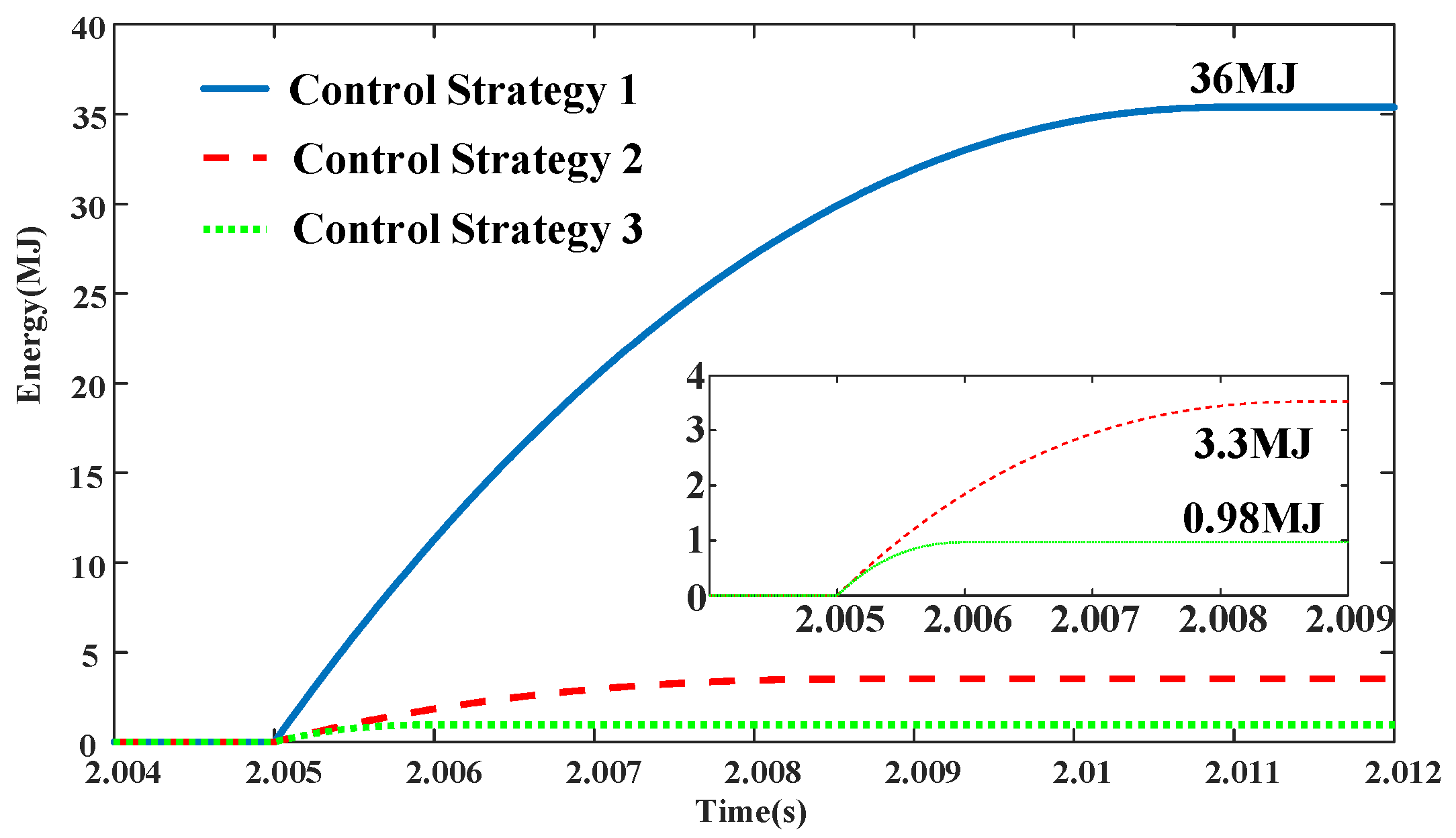
Energy consumption of current-limiting inductor.
Once the fault has been cleared, the inductance L retains 0.5LI32 of the magnetic field energy, and a circulating current is formed with T5. This current must be consumed, and the following method is used. After the fault is cleared, T4b and T1 are triggered, and the voltage across capacitor C is added to both ends of T5, causing it to shut off owing to the reverse voltage. The current then flows through L, T1, C, and T4b to form a loop. The current in the inductor gradually decreases to zero. As L is a 100 millihenry inductance and C is a ten-microfarad capacitor, the voltage across the capacitor returns to the lower positive and upper negative polarities after the discharge of L is complete. At this point, because of the thyristor in the loop, the capacitor no longer discharges, and the energy in the inductor is transferred to the capacitor along with a portion of the energy consumed by resistor R1. T2 and T3b are triggered again, and the remaining energy in the capacitor is consumed by resistor R2. Further refinement may be necessary to ensure optimal system performance.

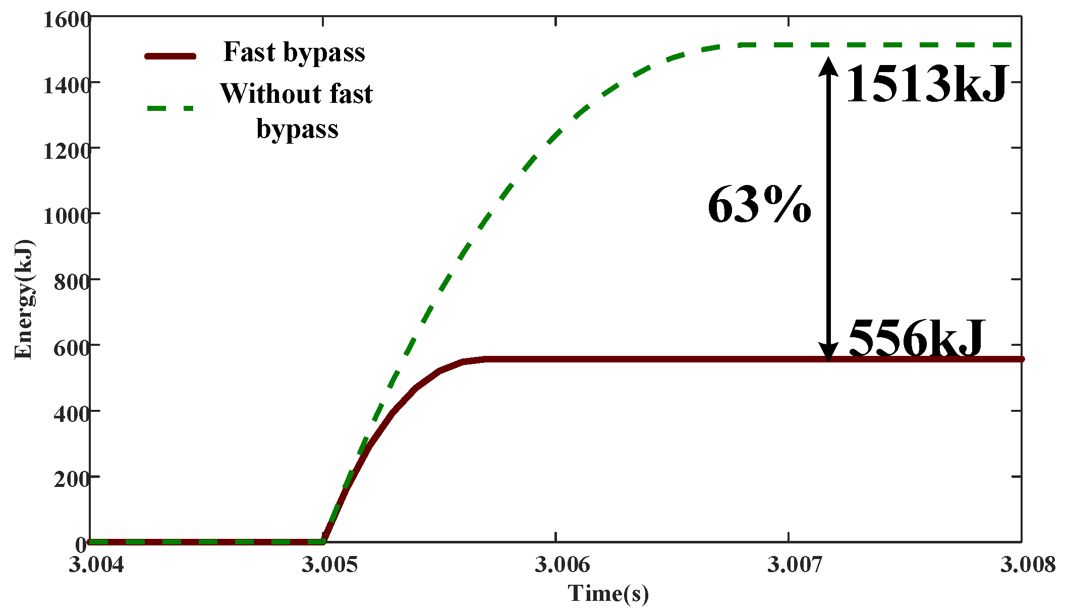
4.2.2. Approximate Calculation of Arrester Energy Consumption Reduction

At time t4, the transfer branch IGBT in the DCCB is controlled to turn off, and the arrester begins to consume energy, assuming that the line current drops to zero at time t5. This period was calculated as Δt3 = t5t4. To calculate the effect of the current-limiting inductor fast bypass on the energy consumption of the arrester, it was necessary to simplify its working characteristics. Figure 15 shows the I–V characteristic curve of the arrester, where V is the unit value of the terminal voltage of the arrester, and its reference value is the rated voltage Umovn of the arrester. When the current flowing through the arrester changes, the voltage at both ends also changes; however, at a current of several kiloamperes, the voltage value can be approximated as kUmovn, where k is a constant. In this study, k was set as 1.92. To ensure a complete representation of the I–V curve, the portion of the graph where the current exceeds 2.8 kA is shown as a dashed line.
Without using the current-limiting inductance fast bypass scheme and ignoring the line impedance and system resistance after DCCB action, the following can be obtained from the KVL:
U dc = ( L + L dc ) d i dc d t + ( R 1 + R 2 ) i dc + k U movn
From (12), it can be obtained that idc(t4) = I3. Combined with (18), the current at this stage can be approximated as:
i dcL _ 1 = I 3 e t / τ L _ 1
In the formula:
{ i dcL _ 1 = I 3 e t / τ L _ 1 τ L _ 1 = L + L dc R 1 + R 2
In the same manner, after adopting the thyristor fast bypass scheme:
{ i dcL _ 0 = I 3 e t / τ L _ 0 τ L _ 0 = L dc R 1 + R 2
At time Δt3, ignoring the energy consumed by the line impedance and system resistance in the above two cases, the following can be obtained through energy conservation:
{ 0 Δ t 3 _ 1 U dc I 3 e t / τ L _ 1 d t + 1 2 ( L + L dc ) I 3 2 = E mov 1 + 0 Δ t 3 _ 1 ( R 1 + R 2 ) I 3 2 e 2 t / τ L _ 1 d t 0 Δ t 3 _ 0 U dc I 3 e t / τ L _ 0 d t + 1 2 L dc I 3 2 = E mov 1 + 0 Δ t 3 _ 0 ( R 1 + R 2 ) I 3 2 e 2 t / τ L _ 0 d t
Emov1 and Emov2 are divided into the energy absorbed by the surge arrester without bypassing the inductor and after bypassing. As the current finally decreases to zero, the integral interval of the integral term in the above formula can be approximated as (0 ∞). From the above formula, it can be observed that the energy consumption reduction in the arrester owing to the bypass of the current-limiting inductance L is
Δ E = U dc I 3 ( τ L _ 1 τ L _ 0 ) + 1 2 L I 3 2 1 2 ( R 1 + R 2 ) I 3 2 ( τ L _ 1 τ L _ 0 )
Since idc is still in the rising stage when DCCB operates, the inductance has to divide the voltage, and thus, Udc > (R1 + R2)I3. It can be seen from Formula (23) that fast bypassing the current-limiting inductance of the line can reduce the energy consumption of the arrester by a considerable extent.

5. Model Validation

5.1. DC System Verification

This section validates the current-limiting method previously discussed for single-ended DC systems. Theoretical and simulation results were compared to confirm the accuracy of the analysis of the current limiter action process. Additionally, the bypass effect of the current-limiting inductor was demonstrated.
The simulation system is illustrated in Figure 16. The rated DC voltage of the system is Udc = 400 kV, the rated DC current is In = 2 kA, and the current-limiting reactor is Ldc = 0.15 H, ignoring the system internal resistance and current-limiting impedance. The parameters of the current limiter are as follows: L = 0.4 H, R1 = 60 Ω, R2 = 20 Ω, C = 20 μF, and the capacitor pre-charge voltage U0 = 100 kV; the I–V curve of the arrester is shown in Figure 15, and the rated voltage is 400 kV. At t = 2.0 s, a unipolar ground fault occurs in the system. When the current exceeds the rated value by 20%, the current limiter is activated. The action of the current limiter is described above. The key parameters of the current-limiting process are shown in Figure 16. In the figure, the simulation results are represented by solid lines, and the numerical calculation results are represented by dotted lines.
It can be seen from Figure 16 that the theoretical numerical calculation results are relatively close to the model simulation results, which proves the correctness of the state analysis in each time period after the current limiter is activated, as described in the Section 2 of this paper. It can be seen from the figure that the capacitor voltage uc is the voltage across the thyristor T3a in the current commutation stage, and the time required for this stage is Δt1 = 600 ns, which can ensure the reliable shutdown of the thyristor. After the current limiter is fully engaged, uc becomes higher than the system voltage by 206 kV, which can ensure that the voltage at both ends of T4a is negative on the left and positive on the right, ensuring its reliable shutdown. The analysis of the above two points proves the rationality of the parameter selection analysis described in the Section 3 of this paper.
In Figure 16, the third figure corresponds to the derivation of the idc value in the Section 2. From the figure, it can be seen that the calculated values of the fault current I0, I1, I2 at each time node proposed in Section 2 have a small error compared to the simulation values. Therefore, it is reasonable to use the mathematical model in Section 2 for the selection of component parameters in Section 3.
Next, we analyzed the consumption of energy stored in the current-limiting inductance L due to the bypass after the circuit breaker operates. As shown in Figure 16, the circuit breaker operates at t = 2.005 s; the inductor current remains unchanged due to the withdrawal of the fault circuit iL by the fast bypass, and the capacitance uc also remains unchanged. Figure 17 and Figure 18 show the changes in the inductor current and capacitor voltage during inductor energy transfer and consumption after the circuit breaker operates. Then, T4b and T1 are triggered at time t6. As iL and uc are in the same direction, the current first increases. After the capacitor discharge ends, the inductor charges the capacitor, and the current decreases. Finally, all the energy in the inductor is transferred to the capacitor, and the capacitor voltage becomes positive at the bottom and negative at the top. T2 and T3b are triggered at t7; the energy in the capacitor is consumed by R2 and its voltage drops to zero. This process is the same as that in the analysis in the Section 4, which proves the correctness of the theoretical analysis.
To verify the performance of the current limit proposed in this study, Figure 19 shows the fault current curves under the two conditions of current limiter action and non-action. It can be observed that the fault current decreases significantly after the current limiter is used. The current will be 12.73 kA less when the current limiter operates 5 ms after the fault occurs than when the current limiter does not operate.
Figure 20 compares the line currents in the two cases in which the current-limiting inductor in the current limiter is bypassed after the DCCB action. It can be seen that if the inductor is still in the loop when the DCCB operates, the DCCB disconnection time is 3.6 ms. After the current-limiting inductor is bypassed, the DCCB disconnection time is 1 ms; that is, the current-limiting inductor bypass technology can reduce the disconnection time by 2.6 ms. Figure 21 compares three control strategies after a fault occurs: (1) the current limiter does not operate; (2) the current limiter operates but the inductor does not bypass; (3) the current limiter operates and the inductor is bypassed. In these three cases, it can be seen that the investment in the current limiter and the application of the current-limiting inductance bypass technology can significantly reduce the energy consumption of the arrester when the DCCB operates and also reduce the cost of the arrester.

5.2. Three-Terminal IPFC DC Side Simulation Verification

Figure 22 shows a schematic of the 400-kV three-terminal IPFC power grid topology, where IPFC1 is the auxiliary control side, and IPFC2 and IPFC3 are the main control sides. The specific parameters are listed in Table 2. When the IPFC operates in the aforementioned state, only a small current passes through the DC side. Using the current limiter parameters determined by the analysis in Section 2, a two-pole short-circuit fault occurs between stations IPFC1 and IPFC2 at t = 3 s. The fault setting between IPFC1 and IPFC2 has a similar conclusion as the fault setting between IPFC1 and IPFC3. In this simulation example, the fault is set between IPFC1 and IPFC2.
Figure 23 shows the simulation results of the main branch current after the fault when the current limiter and DCCB proposed in this study operate and the current-limiting inductor fast bypass strategy described above is adopted. The change in current is the same as that of the current limiter applied to the ideal DC circuit described above. The main difference is that the IPFC works in the state shown in Table 2; the current on the DC line is significantly small, and thus, the current rises approximately from zero after the fault. The time of the capacitor commutation stage is obviously shorter, which is due to the capacitance of the submodule of the converter station.
Figure 24 and Figure 25 show the main current and capacitor voltage, respectively, after the current-limiting inductor was quickly bypassed after the IPFC fault. Its voltage and current changes are the same as those of the current limiter applied to the ideal DC system described in Section 5.1, where the capacitor current ic in Figure 24 has a spike. Triggering T2 and T3b, the capacitor and R2 form a loop, and the remaining energy in the capacitor can be consumed by resistor R2. The current in the energy consumption process is relatively large; however, because of the use of a thyristor control, it can pass through a relatively large current.
To verify the current-limiting effect of the proposed current limiter applied to the IPFC DC side, Figure 26 shows the reverse results of the three cases. In Figure 26, the three cases are as follows: (1) the current limiter does not operate, (2) the current limiter operates but the inductor does not bypass, and (3) the current limiter operates and the inductor is bypassed. When the current limiter was not used, the fault current was suppressed and increased until it reached 6 kA to lock the IPFC submodule. At this time, the discharge circuit is equivalent to a disconnection, and the current changes to zero. Simultaneously, owing to the blockage of the IPFC submodule, the IPFC exits operation and cannot regulate the power flow further.
As shown in Figure 27, when the DCCB operates, the maximum voltages at both ends of the arrester are approximately the same, and the voltage decreases faster when the current-limiting inductor fast-bypass control method is adopted. From the I–V characteristic curve of the arrester, it can be seen that adopting this control strategy can accelerate circuit breaker cutoff and ultimately enable the faster disconnection of the line. Because the current flowing through the arrester is the same as that when the DCCB operates, if the current drops faster, the circuit breaker can disconnect the line faster, and the energy consumption of the arrester will also be significantly reduced. Figure 28 shows the power consumption of the arrester for the two cases. The energy consumption of the surge arrester using the current-limiting inductive fast bypass scheme was 63% lower than that of the unused fast bypass scheme. In short, the current limiter suitable for IPFC proposed in this paper can limit the fault current and significantly reduce it, avoiding the blocking of IPFC submodules due to overcurrent. This causes the IPFC to exit operation, thus losing the control function of line power and the inductor bypass scheme of the current limiter. This reduces the breaking time and energy consumption of the arrester.
The voltage on the DC side will drop after a fault occurs, because the capacitor of the IPFC submodule is discharged through the short circuit; on the DC line without a fault, the current will change owing to the voltage drop, but it will not exceed the operating condition of the circuit breaker. This is because the drop in the DC bus voltage causes a decline in the power control capability of the main control line and fluctuation of the AC line power. After the circuit breaker operates, the auxiliary control-side IPFC loses the ability to control the voltage at its two ends, and the voltage at both ends will be commutated by the IPFC. This is because the main control-side IPFC connected to it loses the connection line with the auxiliary control-side IPFC. Considering the impact of the substation control mode, the auxiliary control-side IPFC re-establishes a stable DC bus voltage, and the other main control-side IPFC converter stations gradually restore the ability to control the power flow of the line.
Figure 29 shows the change in the DC voltage of each IPFC converter station after a fault occurs. Because the circuit breaker cuts off the connection line between the IPFC1 and IPFC2 stations after the circuit breaker, the IPFC2 DC voltage cannot be received by the auxiliary control side after the line is disconnected. In the control of converter station IPFC3, its voltage will eventually increase to approximately 540 kV after a sudden drop. By contrast, IPFC1 is still connected to IPFC3 through a DC line, and its voltage will stabilize at 400 kV after a period of oscillation. In Figure 29, the voltages at stations IPFC1 and IPFC2 exhibit a spike at t = 3.005 s, which is caused by the action of the arrester of the circuit breaker. Figure 30 shows the change in the DC-line current between IPFC1 and IPFC3 after the fault, and the DC-line current between IPFC1 and IPFC3 is described in detail above. As shown, after the fault occurs, the current rises, attenuates, oscillates, and finally returns to the state before the fault occurs. The oscillation attenuation of the current occurs because the IPFC submodule capacitance in the discharge circuit and the current-limiting inductance on the line can be equivalent to a second-order discharge circuit.

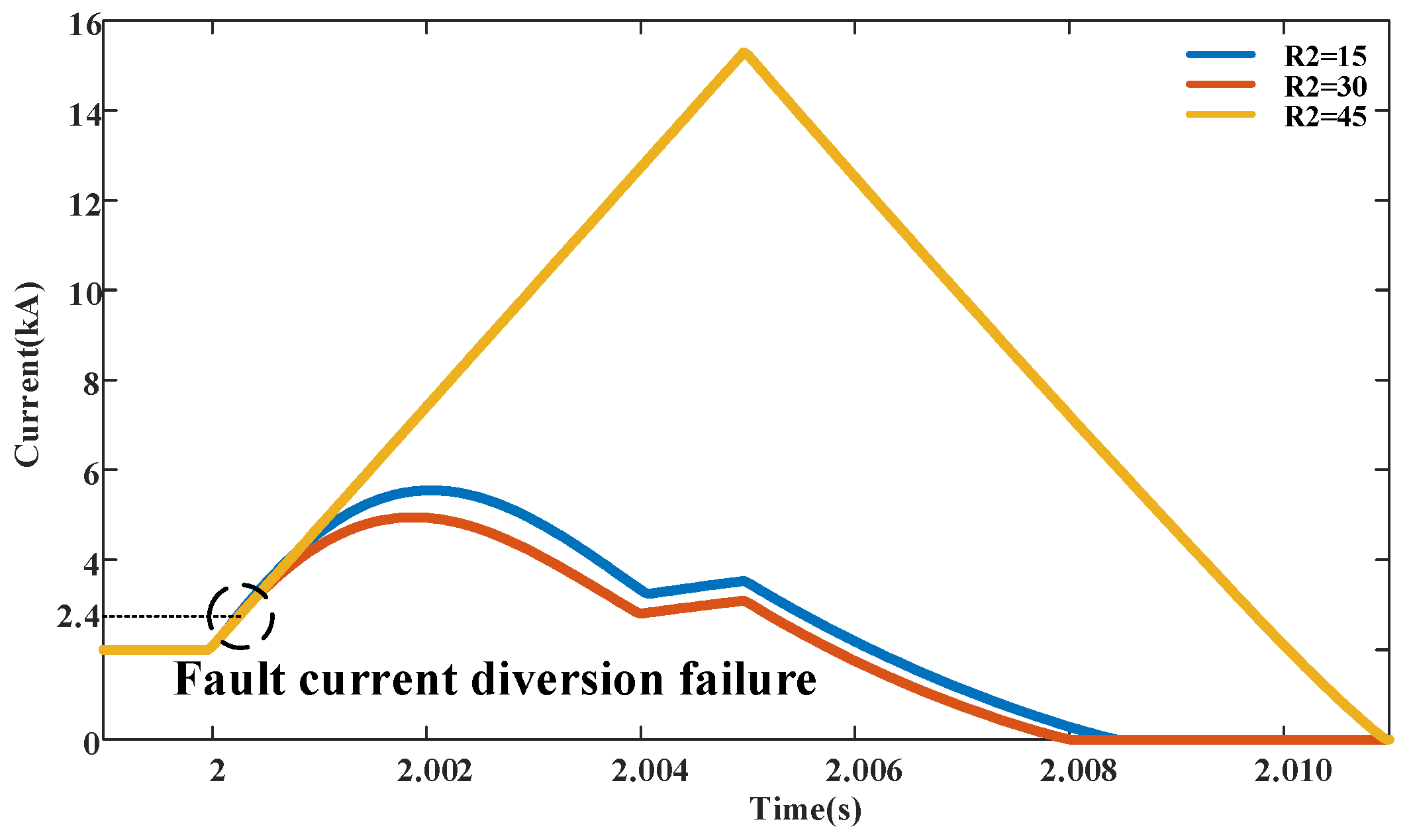
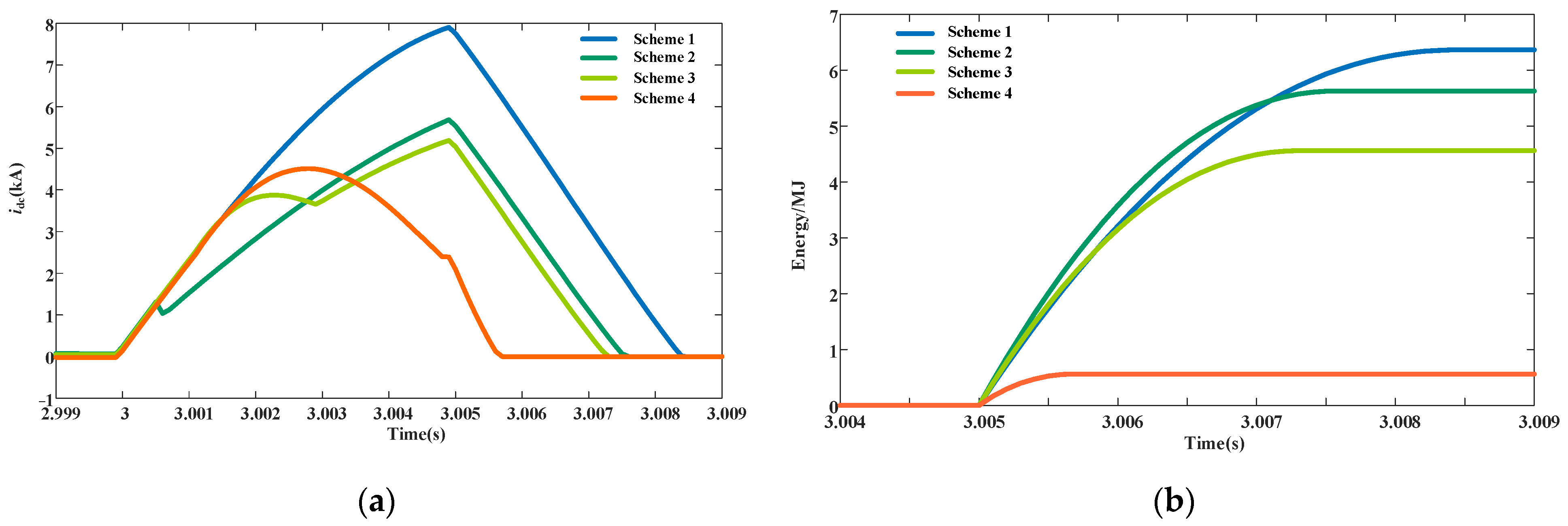
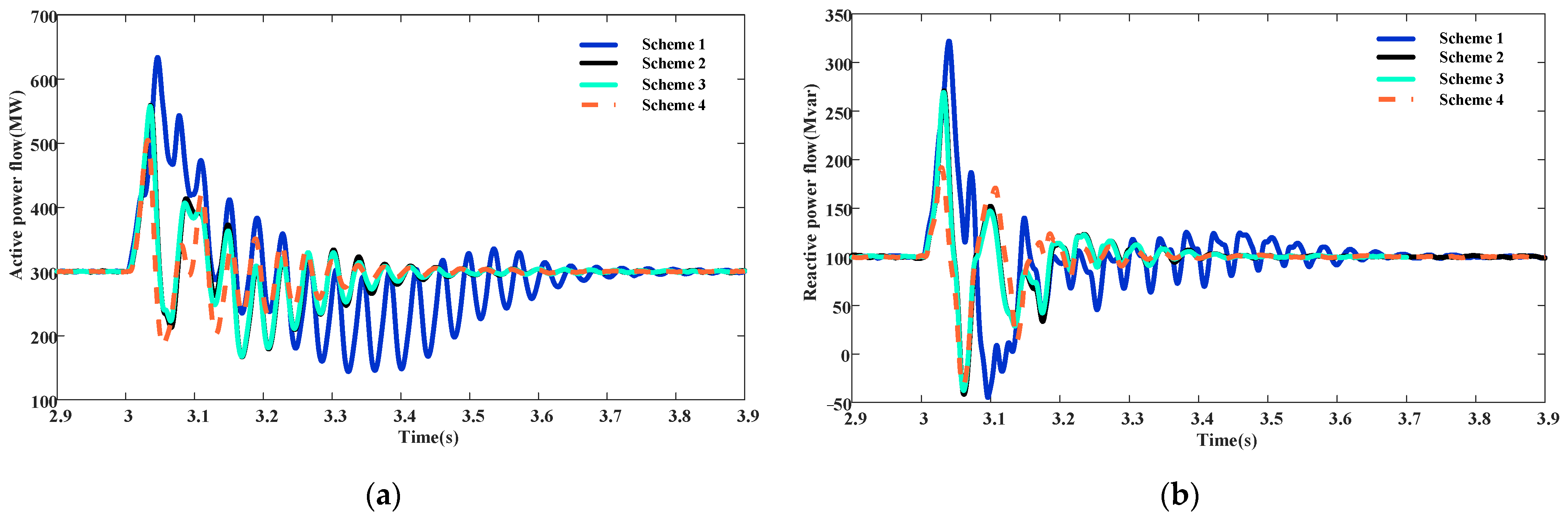
5.3. Comparison and Verification with Other Fault Current Limiters

To further verify the performance of the FCL scheme proposed in this paper, the typical DC circuit breaker proposed by ABB [27] was used as scheme 1. The inductive solid-state fault current limiter proposed in [22] was used as scheme 2, the FCL based on the pre-charge commutation capacitor proposed in [28] was used in scheme 3, and the current limiter proposed in this paper was used as scheme 4 for performance analysis. These four FCLs were built into the three-terminal IPFC system, as shown in Figure 22. The simulation results of the four schemes are shown in Figure 31, with a DC-side fault occurring in the system.
The fault–current waveforms of the four schemes are shown in Figure 31a. Scheme 1 did not use a current-limiting device. The peak value of the fault current is the highest among the four schemes. Schemes 2 and 3 use the surge arrester and phase-change capacitor to force the current to be transferred to the current-limiting branch, and the current-limiting inductor in the current-limiting branch is used to limit the rise in the fault current. Scheme 4 places a pre-charged capacitor into the fault current transfer stage, and the capacitor voltage increases during the transfer process and reduces the voltage difference between the converter station and the line side, forcing the fault current to fall and limiting the fault current peak. At t = 3.005 ms of circuit breaker operation, the fault current drop rates of schemes 1, 2, and 3 are basically the same; scheme 4 adopts the thyristor fast bypass strategy, and the current-limiting inductor exits the current-limiting loop, so the fault current drop rate is fast, and the circuit breaker shutdown time is short.
The surge arrester discharge–energy waveforms for the four schemes of are shown in Figure 31b. In scheme 1, the fault current is the highest, and the arrester needs to discharge all the energy. Moreover, the arrester’s discharge energy requirements are the highest. In scheme 2 and scheme 3, the current-limiting inductor reduces the peak current, thereby reducing the arrester discharge energy. In scheme 3, the current-limiting resistor also consumes part of the energy, which further reduces the discharge energy. In scheme 4, in the bypass current-limiting inductance, the arrester discharge energy is significantly reduced. Scheme 4 adopts the fast bypass strategy of the current-limiting inductor, which significantly reduces the arrester discharge energy.
The three-terminal IPFC system proposed in this study still has one side of the master IPFC that can operate normally after fault resection. The effects on the non-faulty side after fault removal in the four schemes are shown in Figure 32. Figure 32a,b show the control ability of the non-fault-side IPFC for active and reactive power flows, respectively. Among the first three schemes, scheme 4 had the smallest fluctuation in power flow and the fastest recovery. Therefore, scheme 4 can minimize the power system disturbances caused by the fault and is beneficial for power system stability.

6. Conclusions

To assist with the IPFC’s DC-side fault ride-through strategy, this paper proposes a new hybrid current limiter topology, analyzes each stage of its current-limiting process, and proposes a device parameter selection scheme. Based on the above analysis, the following conclusions can be drawn.
(1)
The proposed IPFC current limiter can limit the DC-side short-circuit current below the blocking protection threshold such that a non-blocking fault ride-through can be realized. This improves the survivability of the IPFC under fault conditions.
(2)
The operation loss of the current limiter proposed in this study is low. Compared to other current limiters that use fully controlled devices, the current limiter proposed in this article only uses thyristors, greatly reducing the cost.
(3)
By adopting the thyristor fast bypass scheme proposed in this study, the current limiter can further reduce the energy consumption of the arrester during the circuit breaker operation, which further reduces the investment cost of the circuit breaker.
(4)
After the circuit breaker operates, the IPFC using the proposed strategy can restore the DC voltage stability and control ability in a short time.
(5)
In this paper, we propose and validate an FCL for the IPFC. However, post-fault reclosing and the corresponding control strategies were not studied. Future research should focus on post-fault reclosing and control strategies to enhance the post-fault survivability of the IPFC.

Author Contributions

Investigation, J.L. and B.L.; methodology, J.L.; validation, J.L.; writing—original draft preparation, J.L.; writing—review and editing, J.L., H.S., B.L., Q.J., Y.Y., Y.Z., T.L. and C.N.; supervision, B.L. All authors have read and agreed to the published version of the manuscript.

Funding

This work was supported by the General Project of Natural Science Foundation of Sichuan Province under Grant 2022NSFSC0262. And it is also supported by the Opening Fund of Power Internet of Things Key Laboratory of Sichuan Province (No. PIT-F-202311, The Novel Adaptive Recovery Technology for the New Power Systems Based on Dynamic Measurement).

Data Availability Statement

The raw data supporting the conclusions of this article will be made available by the authors on request.

Conflicts of Interest

The authors declare no conflicts of interest.

References

  1. Wang, Z.; Mu, L. Microgrid Fault Detection Method Coordinated with a Sequence Component Current-Based Fault Control Strategy. Prot. Control Mod. Power Syst. 2024, 9, 81–93. [Google Scholar] [CrossRef]
  2. Simatupang, D.P.; Choi, J. Integrated Photovoltaic Inverters Based on Unified Power Quality Conditioner with Voltage Compensation for Submarine Distribution System. Energies 2018, 11, 2927. [Google Scholar] [CrossRef]
  3. Simatupang, D.P.; Choi, J. PV Source Inverter with Voltage Compensation for Weak Grid Based on UPQC Configuration. In Proceedings of the 2018 IEEE 18th International Power Electronics and Motion Control Conference (PEMC), Budapest, Hungary, 26–30 August 2018; pp. 421–427. [Google Scholar]
  4. Xie, B.; Li, Z.; An, Y.; Zhao, J. The Coordinated Droop Control Strategy for Interline Power Flow Controller. In Proceedings of the 2022 IEEE 6th Conference on Energy Internet and Energy System Integration (EI2), Chengdu, China, 11–13 November 2022; pp. 849–852. [Google Scholar]
  5. Sau-Bassols, J.; Zhao, Q.; García-González, J.; Prieto-Araujo, E.; Gomis-Bellmunt, O. Optimal Power Flow Operation of an Interline Current Flow Controller in an Hybrid AC/DC Meshed Grid. Electr. Power Syst. Res. 2019, 177, 105935. [Google Scholar] [CrossRef]
  6. Ebeed, M.; Kamel, S.; Jurado, F. Determination of IPFC Operating Constraints in Power Flow Analysis. Int. J. Electr. Power Energy Syst. 2016, 81, 299–307. [Google Scholar] [CrossRef]
  7. Ghorbani, A.; Soleymani, S.; Mozafari, B. A PMU-Based LOE Protection of Synchronous Generator in the Presence of GIPFC. IEEE Trans. Power Deliv. 2016, 31, 551–558. [Google Scholar] [CrossRef]
  8. Yanfang, F.; Yuehua, L.; Long, M.; Zhijun, C. Research on Specific Fault Analysis and Protection Countermeasures of AC/DC Hybrid System. In Proceedings of the 16th IET International Conference on AC and DC Power Transmission (ACDC 2020), Online, 2–3 July 2020; Volume 2020, pp. 1910–1915. [Google Scholar]
  9. Liu, G.; Xu, F.; Xu, Z.; Zhang, Z.; Tang, G. Assembly HVDC Breaker for HVDC Grids With Modular Multilevel Converters. IEEE Trans. Power Electron. 2017, 32, 931–941. [Google Scholar] [CrossRef]
  10. Taherzadeh, E.; Radmanesh, H.; Javadi, S.; Gharehpetian, G.B. Circuit Breakers in HVDC Systems: State-of-the-Art Review and Future Trends. Prot. Control Mod. Power Syst. 2023, 8, 38. [Google Scholar] [CrossRef]
  11. Wang, Y.; Yuan, Z.; Wen, W.; Ji, Y.; Fu, J.; Li, Y.; Zhao, Y. Generalised Protection Strategy for HB-MMC-MTDC Systems with RL-FCL under DC Faults. IET Gener. Transm. Distrib. 2018, 12, 1231–1239. [Google Scholar] [CrossRef]
  12. Lin, W.; Jovcic, D.; Nguefeu, S.; Saad, H. Protection of Full Bridge MMC DC Grid Employing Mechanical DC Circuit Breakers. In Proceedings of the 2017 IEEE Power & Energy Society General Meeting, Chicago, IL, USA, 16–20 July 2017; pp. 1–5. [Google Scholar]
  13. Wang, T.; Chu, X.; Hussain, K.S.T.; Gao, J. Fault Control and Line Protection Strategy for LVDC Microgrids Based on Modified High-Frequency-Link DC Solid State Transformer. Int. J. Electr. Power Energy Syst. 2022, 140, 108052. [Google Scholar] [CrossRef]
  14. Xu, J.; Wu, D.; Li, J.; Zhao, X.; Jia, X. The Voltage Clamping Based DC Circuit Breaker With Decoupled Fault Isolation and Energy Dissipation Processes. IEEE Trans. Power Deliv. 2021, 36, 64–73. [Google Scholar] [CrossRef]
  15. Pan, Y.; Chen, L.; Yuan, Z.; Xu, M.; Liu, L.; Li, G. Research on Current Limiting and Energy Limiting Technology for DC Power Grid Fault. Proc. CSEE 2020, 40, 2006–2015. [Google Scholar] [CrossRef]
  16. Zhu, J.; Zeng, Q.; Guo, X.; Jia, H.; Cui, B.; Wei, T. Multiport Current Injection Hybrid DC Circuit Breaker With Simple Bridge Arm Circuit. IEEE Trans. Ind. Electron. 2023, 70, 9882–9892. [Google Scholar] [CrossRef]
  17. Wang, W.; Barnes, M.; Marjanovic, O.; Cwikowski, O. Impact of DC Breaker Systems on Multiterminal VSC-HVDC Stability. IEEE Trans. Power Deliv. 2016, 31, 769–779. [Google Scholar] [CrossRef]
  18. Beerten, J.; D’Arco, S.; Suul, J.A. Identification and Small-Signal Analysis of Interaction Modes in VSC MTDC Systems. IEEE Trans. Power Deliv. 2016, 31, 888–897. [Google Scholar] [CrossRef]
  19. Xia, D.; Qiu, Q.; Zhang, Z.; Liu, S.; Xia, Z. Magnetic Field and Characteristic Analysis of the Superconducting Fault Current Limiter for DC Applications. IEEE Trans. Appl. Supercond. 2018, 28, 5601405. [Google Scholar] [CrossRef]
  20. Steurer, M.; Frohlich, K.; Holaus, W.; Kaltenegger, K. A Novel Hybrid Current-Limiting Circuit Breaker for Medium Voltage: Principle and Test Results. IEEE Trans. Power Deliv. 2003, 18, 460–467. [Google Scholar] [CrossRef]
  21. Ma, T.; Dai, S.; Song, M.; Li, C. Electromagnetic Design of High-Temperature Superconducting DC Bias Winding for Single-Phase 500 kV Saturated Iron-Core Fault Current Limiter. IEEE Trans. Appl. Supercond. 2018, 28, 5200805. [Google Scholar] [CrossRef]
  22. Fereidouni, A.R.; Vahidi, B.; Hosseini Mehr, T. The Impact of Solid State Fault Current Limiter on Power Network With Wind-Turbine Power Generation. IEEE Trans. Smart Grid 2013, 4, 1188–1196. [Google Scholar] [CrossRef]
  23. Radmanesh, H.; Fathi, S.H.; Gharehpetian, G.B.; Heidary, A. Bridge-Type Solid-State Fault Current Limiter Based on AC/DC Reactor. IEEE Trans. Power Deliv. 2016, 31, 200–209. [Google Scholar] [CrossRef]
  24. Jeong, J.-S.; Choi, H.-S. A Study on Increasing the Capacity of Transformer-Type Superconducting DC Circuit Breaker. IEEE Trans. Appl. Supercond. 2023, 33, 5500405. [Google Scholar] [CrossRef]
  25. Yang, S.; Xiang, W.; Lu, X.; Zuo, W.; Wen, J. An Adaptive Reclosing Strategy for MMC-HVDC Systems With Hybrid DC Circuit Breakers. IEEE Trans. Power Deliv. 2020, 35, 1111–1123. [Google Scholar] [CrossRef]
  26. Tao, C.; Wang, W.; Li, T.; Zhang, J. Current Limiting Hybrid DC Circuit Breaker Based on Capacitor Commutation. Dianwang JishuPower Syst. Technol. 2023, 47, 5138–5146. [Google Scholar] [CrossRef]
  27. Bucher, M.K.; Wiget, R.; Andersson, G.; Franck, C.M. Multiterminal HVDC Networks—What Is the Preferred Topology? IEEE Trans. Power Deliv. 2014, 29, 406–413. [Google Scholar] [CrossRef]
  28. Zhang, C.; Wu, D.; Chen, K.; Li, J.; Xu, J.; Zhao, C. DC Fault Current Limiter Based on Precharge Commutation Capacitor. Zhongguo Dianji Gongcheng Xuebao Proc. Chin. Soc. Electr. Eng. 2019, 39, 54–62. [Google Scholar] [CrossRef]
Figure 1. Two-terminal IPFC system.
Electronics 13 01038 g001
Figure 2. Submodule capacitive discharge equivalent circuit.
Electronics 13 01038 g002
Figure 3. Current limiter topology.
Electronics 13 01038 g003
Figure 4. DC line fault equivalent circuit.
Electronics 13 01038 g004
Figure 5. t0t1 fault current path.
Electronics 13 01038 g005
Figure 6. Fault current path during t1t2 period.
Electronics 13 01038 g006
Figure 7. Fault current path during t2t3 period.
Electronics 13 01038 g007
Figure 8. Fault current path during t3t4 period.
Electronics 13 01038 g008
Figure 9. Fault current limiter control action process.
Electronics 13 01038 g009
Figure 10. Influence of resistor R2 on the current-limiting effect.
Electronics 13 01038 g010
Figure 11. Effect of capacitance on Δt1.
Electronics 13 01038 g011
Figure 12. Relationship between C, Δt2, and idc_max.
Electronics 13 01038 g012
Figure 13. Voltage variations for different commutation capacitors.
Electronics 13 01038 g013
Figure 14. Capacitor charging scheme.
Electronics 13 01038 g014
Figure 15. Arrester I–V curve.
Electronics 13 01038 g015
Figure 16. Comparison of theoretical calculation results and simulation results in the current-limiting process.
Electronics 13 01038 g016
Figure 17. Current through the current-limited inductor.
Electronics 13 01038 g017
Figure 18. Commutation capacitor voltage.
Electronics 13 01038 g018
Figure 19. Comparison of current-limiting effect.
Electronics 13 01038 g019
Figure 20. Comparison of currents for different control strategies.
Electronics 13 01038 g020
Figure 21. Comparison of the arrester energy consumption under different control strategies.
Electronics 13 01038 g021
Figure 22. Schematic of three-terminal IPFC grid.
Electronics 13 01038 g022
Figure 23. Key current value after current limiter action.
Electronics 13 01038 g023
Figure 24. Critical current value after current limiter fast bypass.
Electronics 13 01038 g024
Figure 25. Commutation capacitor voltage after current limiter fast bypass.
Electronics 13 01038 g025
Figure 26. Current comparison under different conditions.
Electronics 13 01038 g026
Figure 27. Comparison of surge arrester voltages under different conditions.
Electronics 13 01038 g027
Figure 28. Energy consumption of arresters under different conditions.
Electronics 13 01038 g028
Figure 29. DC-side voltages at each converter station.
Electronics 13 01038 g029
Figure 30. Nonfaulted line current after fault.
Electronics 13 01038 g030
Figure 31. (a) Comparison of fault currents; (b) comparison of arrester energy consumption.
Electronics 13 01038 g031
Figure 32. (a) Active power flow; (b) reactive power flow.
Electronics 13 01038 g032
Table 1. Each time node and characteristics of the current limiter.
Time FrameNode Features
t0Time of failure
t1Fault detected
t2uc = 0; the capacitor has just discharged
t3i1 = idc; ic = 0; the current limiter is fully engaged
t4DCCB action
Table 2. DC grid parameters.
Converter StationNumber of Bridge Arm SubmodulesSubmodule Capacitance/μFBridge Arm Reactance/mHControl Strategy
IPFC12003000100Udc = 400 kV
Q = 0 MVar
IPFC22003000100P = 400 MW
Q = 200 MVar
IPFC32003000100P = 300 MW
Q = 100 MVar
Disclaimer/Publisher’s Note: The statements, opinions and data contained in all publications are solely those of the individual author(s) and contributor(s) and not of MDPI and/or the editor(s). MDPI and/or the editor(s) disclaim responsibility for any injury to people or property resulting from any ideas, methods, instructions or products referred to in the content.

