Article

Enhancing the Performance of GaN-Based Light-Emitting Diodes by Incorporating a Junction-Type Last Quantum Barrier

School of Integrated Circuits, Anhui University, Hefei 230601, China
*
Authors to whom correspondence should be addressed.
Electronics 2024, 13(7), 1399; https://doi.org/10.3390/electronics13071399
Submission received: 15 March 2024 / Revised: 3 April 2024 / Accepted: 4 April 2024 / Published: 8 April 2024

Abstract

:
In this paper, an n-i-p-type GaN barrier for the final quantum well, which is closest to the p-type GaN cap layer, is proposed for nitride light-emitting diodes (LEDs) to enhance the confinement of electrons and to improve the efficiency of hole injection. The performances of GaN-based LEDs with a traditional GaN barrier and with our proposed n-i-p GaN barrier were simulated and analyzed in detail. It was observed that, with our newly designed n-i-p GaN barrier, the performances of the LEDs were improved, including a higher light output power, a lower threshold voltage, and a stronger electroluminescence emission intensity. The light output power can be remarkably boosted by 105% at an injection current density of 100 A/cm2 in comparison with a traditional LED. These improvements originated from the proposed n-i-p GaN barrier, which induces a strong reverse electrostatic field in the n-i-p GaN barrier. This field not only enhances the confinement of electrons but also improves the efficiency of hole injection.

1. Introduction

Nitride light-emitting diodes (LEDs) have garnered increasing attention and extensive amounts of research due to their low power consumption and compact size [1,2,3]. One common problem facing GaN-based LEDs is that the electrons can be easily injected from the active regions into the p-GaN region, which decreases the recombination of the carriers within the active regions, owing to the high mobility and small effective mass of the electrons. This issue significantly limits these devices’ performances. To solve this problem, a novel electron-blocking layer (EBL) made of AlGaN with a wide band gap was inserted among the active regions and the p-type GaN cap region [4,5,6,7,8]. However, this method alone is not effective in suppressing the injection of the electrons to the p-type GaN cap layer. Moreover, it creates an obstruction within the movement of holes from the p-type GaN cap layer towards the active regions. To enhance the efficacy of hole injection from the p-GaN region into the active regions, concepts such as AlInGaN EBL [9], undope BGaN/BAlN EBL [10,11], Graded EBL [12,13], quantum barrier [14], triangular EBL [15], and band offset [16] devices have been reported. These works focused on finding a proper EBL, which in general required an additional hetero epitaxial deposition, making them difficult to realize due to the lattice mismatch. The EBL is primarily utilized for engineering the energy band of the multiple quantum wells (MQWs) in close proximity to the p-GaN cap layer, thereby enhancing both electron and hole concentrations and subsequently improving the electrical and optical characteristics of nitride LEDs [17,18,19,20].
The aforementioned studies show that researchers have enhanced the carrier injection efficiency by improving wider-bandgap EBL, but for GaN-based LEDs, it is not sufficient to optimize a single p-EBL. Alternatively, it is conceivable that a favorable polarization charge may exist at the interface where the final quantum barrier meets the EBL with a wider bandgap. This occurrence can be attributed to a negative difference in heterointerface polarization [21]. The existence of this positive charge has an effect on bending the last quantum barrier bands, leading to a reduction in the effective electron barrier and an increase in the effective hole barrier. Consequently, it may significantly compromise both the electron blocking and hole injection processes, ultimately resulting in a diminished optical power and efficiency [22]. As a result, many strategies aimed at improving the amount of droop utilize either an Al composition gradient [23,24,25] or a final barrier with a different thickness [23,26,27] as a workaround for this issue. In a previous study we reported high-performance green LEDs employing heterojunction-type last quantum barrier layers [28]. However, the realization of this process is difficult due to lattice structure mismatch. Further investigations are necessary to determine a straightforward device structure that exhibits a mechanism that clearly leads to enhanced carrier injection and reduced current leakage.
In this study, we introduce a novel n-i-p-type GaN barrier to engineer the energy band structure. This n-i-p barrier is used for the last quantum well (QW) only, which is nearest to the p-type GaN cap region. The improvements in the hole injection efficiency and electron confinement of the LED with our newly designed barrier are demonstrated in simulations. In addition, this method can avoid any additional hetero epitaxial growth, which makes it easy to apply in practice.

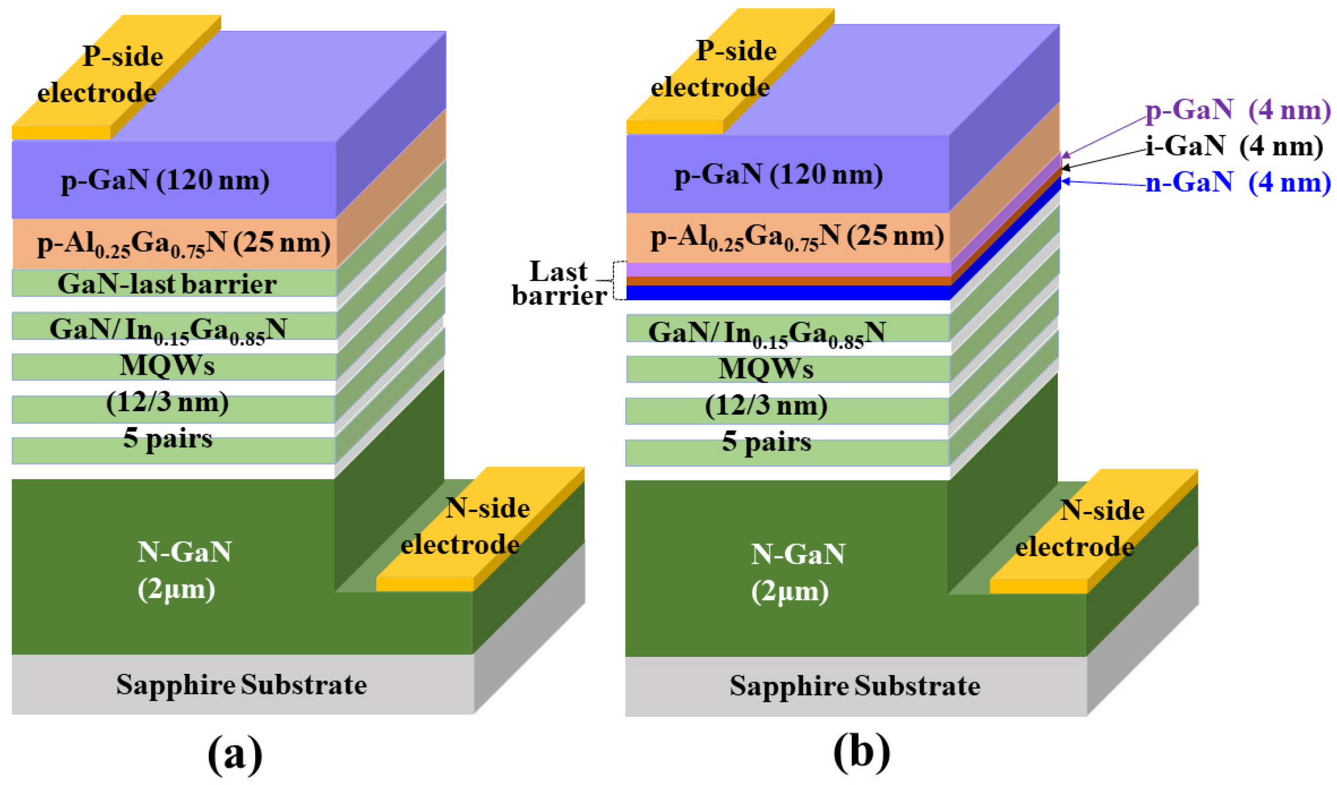
2. Device Structure and Parameters

In this study, the InGaN/GaN MQW LED with a traditional GaN barrier developed in Ref. [29] was used as a reference. Its schematic cross section is shown in Figure 1. From the bottom to the top, the device structure consists of a sapphire substrate, an n-type GaN/Si layer with a concentration of 5 × 1018 cm−3 and a thickness of 2 μm, five periods of GaN (12 nm)/In0.15Ga0.85N (3 nm) MQW regions, subsequently accompanied by a p-type Al0.25Ga0.75N:Mg EBL with a density of 3 × 1017 cm−3 and a thickness of 25 nm, and a 0.12 μm p-type GaN/Mg cap layer with a density of 3 × 1017 cm−3. The dimensions of the device are 60 μm × 60 μm, forming a square shape. When the GaN barrier in the final QW is substituted with n-GaN (1 × 1018 cm−3)-i-GaN-p-GaN (5 × 1018 cm−3), an LED with our proposed n-i-p GaN barrier is then formed, as shown in Figure 1. The thicknesses of the n, I, and p layers in the proposed barrier are identical at 4 nm. Therefore, the only structural difference between these two types of LEDs is the type of barrier used for the last QW.
To examine the impact of the n-i-p GaN barrier on the device’s performance, models of these two types of LEDs were built in Silvaco ATLAS software (version 5.19.20.R), and simulations of the band diagrams, the carrier concentrations, the light output power, the I–V curve, and the electroluminescence spectra were performed. In the calculations, an approximate value of 1 ns was assigned to the Shockley–Read–Hall (SRH) lifetime of the quantum wells (QWs). The coefficient for Auger recombination was assumed to be around 3.0 × 10⁻²⁹ cm6/s. The offset caused by fixed defects and additional interface charges was taken into account in 30% of the theoretical values.
The simulation model incorporates a k·p–Schrödinger solver for the examination of luminescence and carrier distribution in the quantum wells, alongside a semi-classical drift diffusion transport solver [30,31]. It has undergone improvements to accurately capture the luminescence and transport characteristics specific to GaN-based MQW LEDs. A Newton solver is employed to achieve a combined solution of models in both real and energy domains. The Gummel iteration guarantees adherence to the k·p–Schrödinger model by ensuring self-consistency.
The equations that generally dictate the calculation of band gap energies in InGaN and AlGaN are provided below [32].
E g ( I n x G a 1 x N ) = E g ( I n N ) x + E g ( G a N ) ( 1 x ) 3.8 x ( 1 x ) E g ( A l x G a 1 x N ) = E g ( A l N ) x + E g ( G a N ) ( 1 x ) 1.3 x ( 1 x )
InN, GaN, and AlN have band gap energies denoted as Eg(InN), Eg(GaN), and Eg(AlN) with values of 0.77 eV, 3.42 eV, and 6.25 eV, correspondingly. The assumed band–offset ratio for InGaN and AlGaN materials is 0.7/0.3 [33,34].
The determination of the permittivity of nitrides can be achieved by employing linear interpolations, which rely on the values obtained for binary compounds, to establish a relationship with the composition fraction denoted as x [35].
ε ( I n x G a 1 x N ) = 15.3 x + 8.9 ( 1 x ) ε ( A l x G a 1 x N ) = 8.5 x + 8.9 ( 1 x )
Polarization modeling is of the utmost importance in the evaluation of GaN-based devices’ performance. Their highly polar nature results in a significant accumulation of fixed charges at the interfaces, leading to the generation of a substantial static field which is present within the LED. The overall macroscopic polarization P of InGaN (AlGaN) is defined as the combination of the spontaneous polarization PSP in the equilibrium lattice and the piezoelectric polarization PPi induced by strain. The total polarization, P, is given by:
P = P S P + P P i
where PSP is specified in Table 1. Ternary material values are obtained through linear interpolation based on the values of the binary materials.
The piezoelectric polarizations of InGaN and AlGaN are contingent upon the strains present within the materials, which can be mathematically expressed as follows [36,37]:
P P i = 2 a s a 0 a 0 ( e 31 C 13 C 33 e 33 )
where e31 and e33 represent piezoelectric constants, C13 and C33 denote the elastic constants, and a0 corresponds to the wurtzite lattice constant (as is the substrate value). The material parameters for binary compounds are provided in Table 1. In the case of ternary compounds, a linear interpolation method can be employed to estimate these values.
Table 1. Room-temperature polarization parameters of wurtzite nitride semiconductors [32,38].
ParameterSymbolUnitInNGaNAlN
Spontaneous polarizationPspC m−2−0.042−0.034−0.09
Piezoelectric constant (z)e33C m−20.8100.6701.50
Piezoelectric constant (x, y)e31C m−2−0.410−0.340−0.53
Elastic constantC33GPa200392382
Elastic constantC13GPa94100127
Lattice constanta0Å3.5483.1893.112
The physical parameters set in our simulation are justified by reproducing the experimental results in [29], as shown in Figure 2. The simulated results align harmoniously with the measurements, thereby validating the chosen physical parameters.

3. Results and Discussion

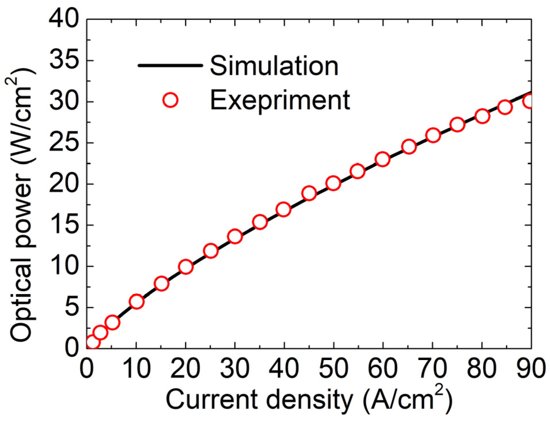
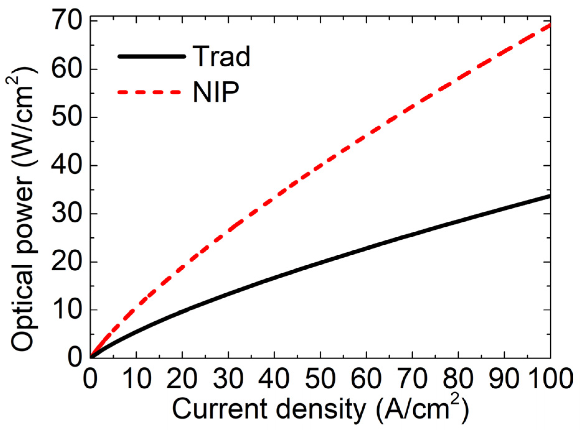
3.1. Light Output Power

The light output power performances of these two types of LEDs have been calculated and compared, as depicted in Figure 3. It is evident that the incorporation of an n-i-p GaN barrier greatly enhances the luminous output capability of the LED, across all levels of current injection. With an n-i-p GaN barrier, the output power density of the LED is increases by 105% in contrast with the traditional one at an injection current density of 100 A/cm2.

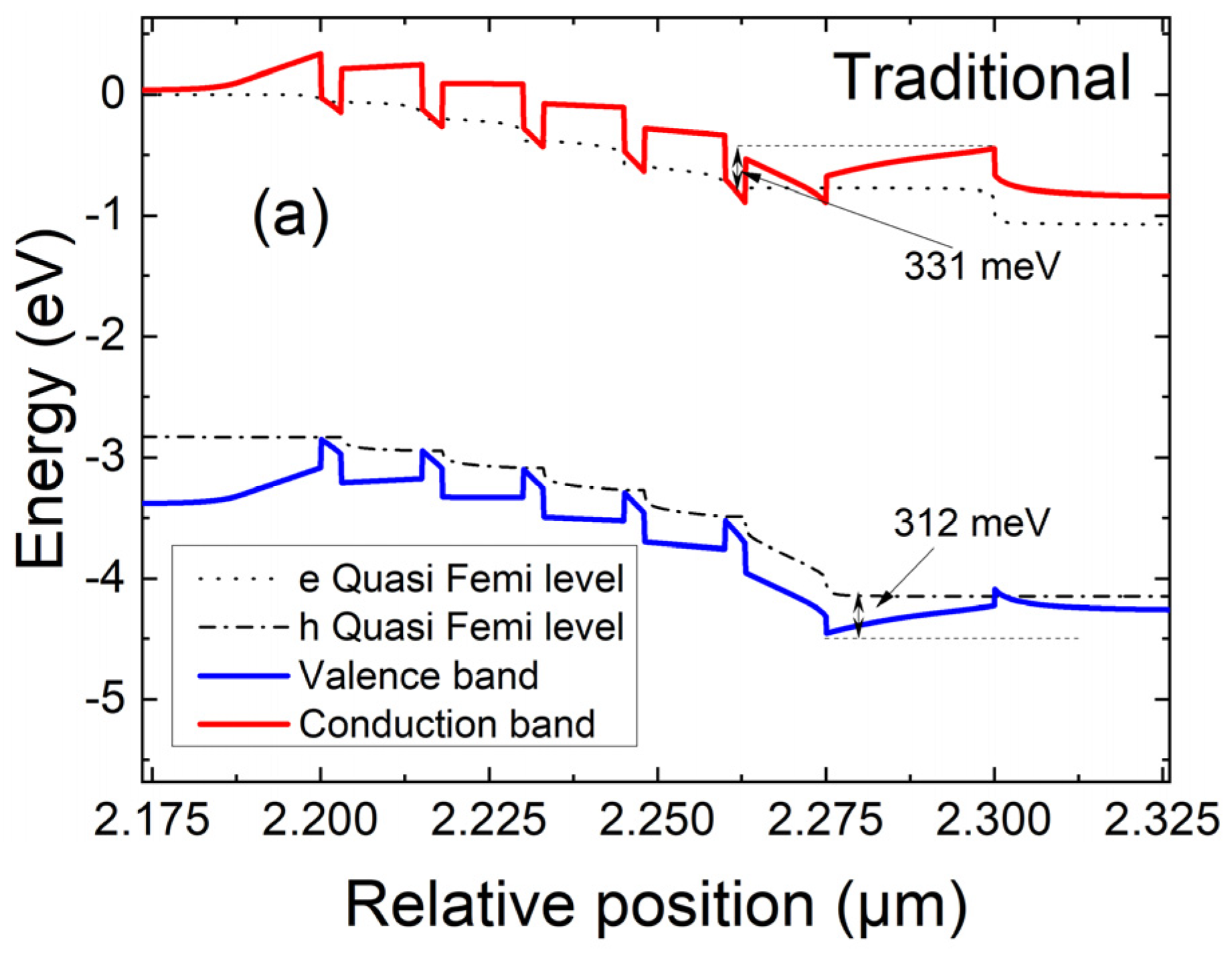
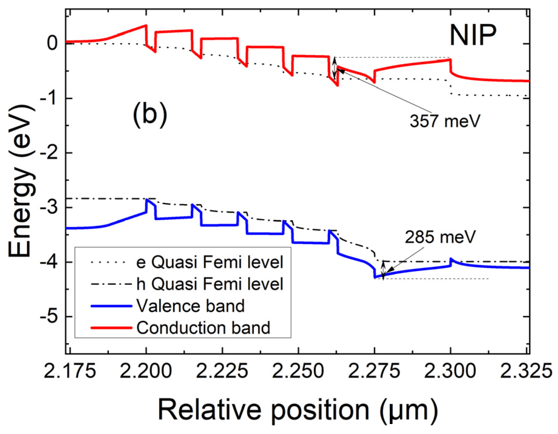
3.2. Energy Band Diagrams

To investigate the carrier transport in LEDs, simulations of the band diagram have been performed. The band diagrams of the LEDs, both with a traditional GaN barrier and an n-i-p GaN barrier, were simulated and results obtained at an injection current density of 40 A/cm2, as depicted in Figure 4. It is evident that, in the case of a traditional GaN barrier, the effective valence band barrier height for the holes is 312 meV, as depicted in Figure 4a. And in the case of an n-i-p GaN barrier, the barrier height for the holes in the valence band is found to be 285 meV, as depicted in Figure 4b. This means that the holes encounter a much lower barrier height in the LED with an n-i-p GaN barrier than in the traditional GaN barrier. Therefore, with an n-i-p GaN barrier, the holes can move from the cap layer to the active regions easier, resulting in a higher efficiency of injecting holes. It is clear that incorporating an n-i-p GaN barrier leads to an increased effective potential barrier height being experienced by the electrons in the conduction band. This increased electron barrier height can effectively suppress the electron leakage from the QWs to the p-type cap region. In summary, the LED with an n-i-p GaN barrier shows significantly improved carrier transport not only in the confinement of electron but also in the injection of holes.

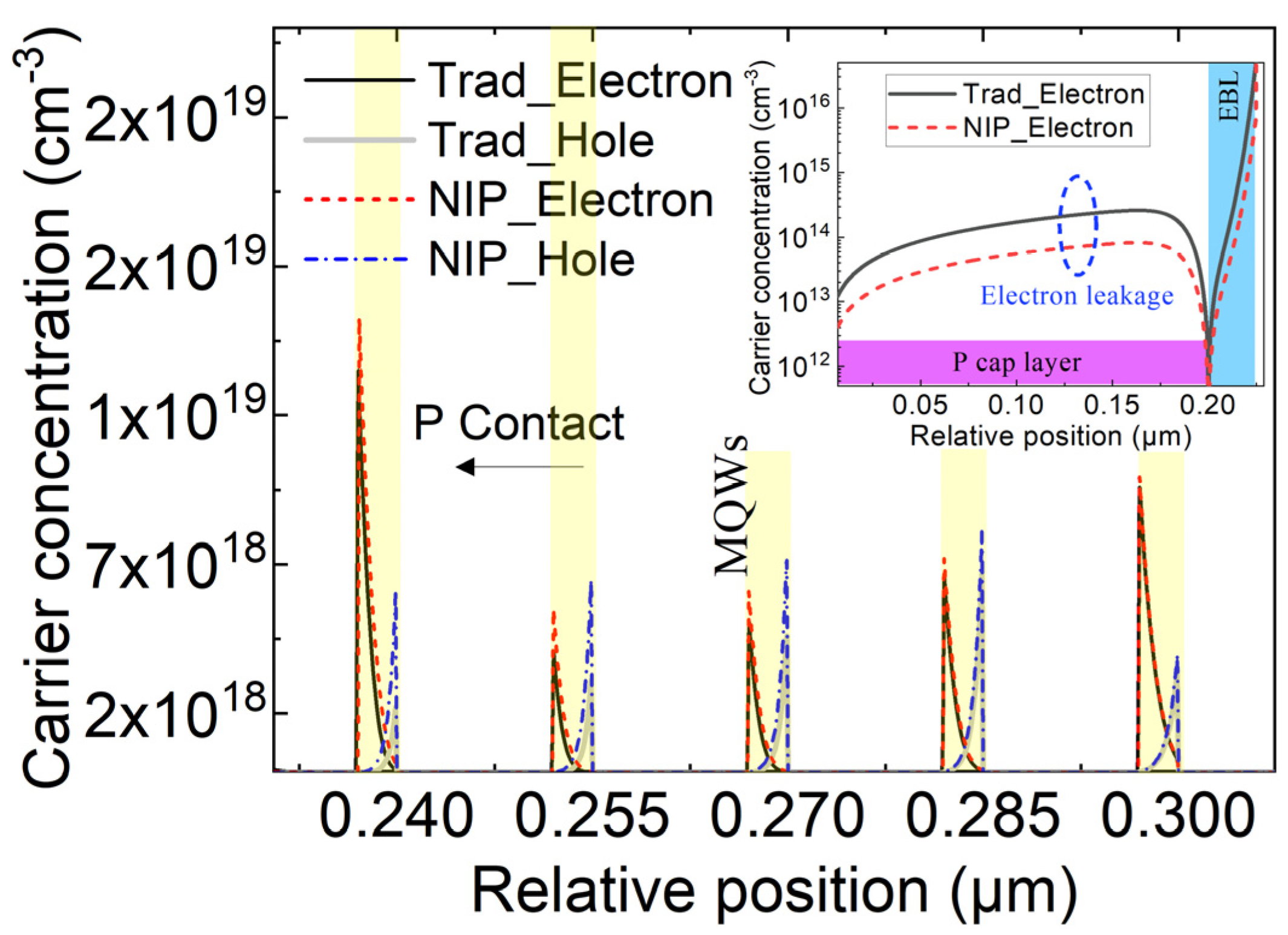
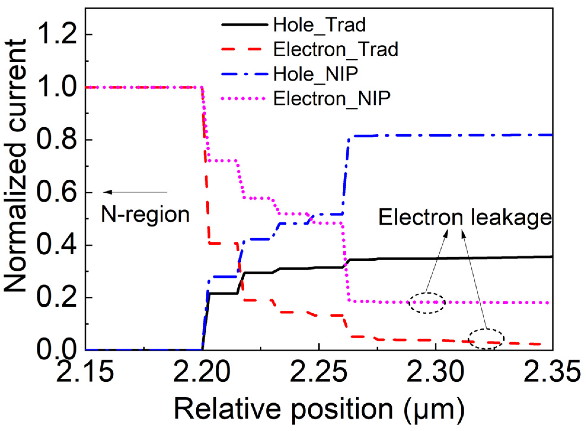
3.3. Carrier Concentration

From the above band diagram analysis, it can be inferred that the n-i-p GaN barrier enhances hole injection. To verify this, we have studied the carrier concentrations in the active regions and compared the distributions of holes and electrons under DC bias. Figure 5 shows the calculated hole and electron distributions of these two types of LEDs at a current density of 40 A/cm2. The reference point for the relative position is established at the uppermost layer of p-GaN, directed in a downward vertical orientation towards the MQWs. As expected, the LED featuring an n-i-p GaN barrier exhibits significantly elevated hole and electron concentrations compared to the LED employing a traditional GaN barrier. In the case of an n-i-p GaN barrier, the peak hole concentration can reach 6.0 × 1018 cm−3 in the first QW. However, in the case of a traditional GaN barrier, the peak hole concentration is only 2.2 × 1018 cm−3 in the first QW, as depicted in Figure 5. It is evident that the electron concentrations in the first QW are also improved with the n-i-p GaN barrier. Similar trends were observed for the other four QWs, although these are not shown in this paper.
The insert in Figure 5 shows the profiles of leaked electronics for a traditional LED and our proposed LED. The traditional LED exhibits a significant electron current leakage, which is about three times higher than our proposed LED. Based on the results shown in Figure 6, it is evident that the electron leakage of the LED utilizing the n-i-p GaN final barrier is significantly lower compared to that of the conventional structure LED. This means that the electron reflection is much stronger than the electron crossing at the EBL. Consequently, our proposed LED structure exhibited a superior performance, as can be seen in Figure 3. The electron-blocking capabilities of the n-i-p GaN barrier were significantly enhanced, leading to a substantial reduction in leakage rate. These data validate that the incorporation of the n-i-p GaN barrier effectively suppresses electron leakage and enhances hole injection efficiency. Therefore, the active regions experienced a simultaneous rise in the concentrations of both electrons and holes.

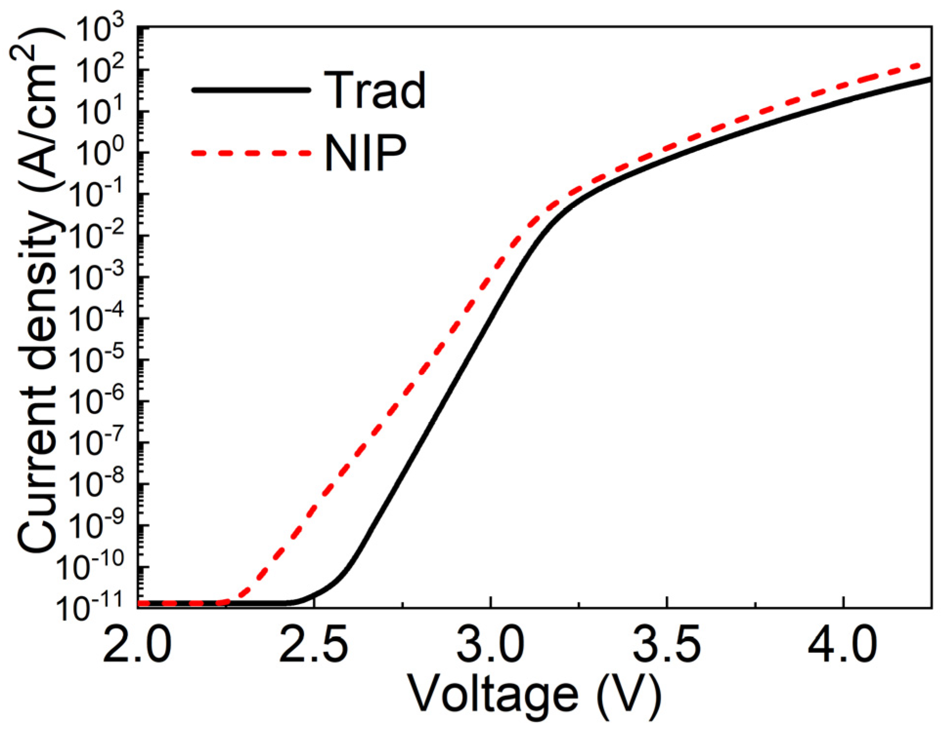
3.4. Current-Voltage Curves

Figure 7 shows the I-V curves of these two types of LEDs. It is evident that the LED featuring an n-i-p GaN final barrier exhibits a reduced turn-on voltage, indicating an improved carrier transport. These results align with the analysis of the band diagram. When the biased forward voltage increases to approximately 4.0 V, the corresponding current densities of traditional and our proposed LED reach 17.4 and 42.212 A/cm2, respectively. Due to the reduced series resistance of the n-i-p GaN final barrier in our proposed LED, the current density of this new structure LED is higher than that of traditional one. It was found that the electrical characteristics were hampered by adding the n-i-p-type doping from our proposed LED.

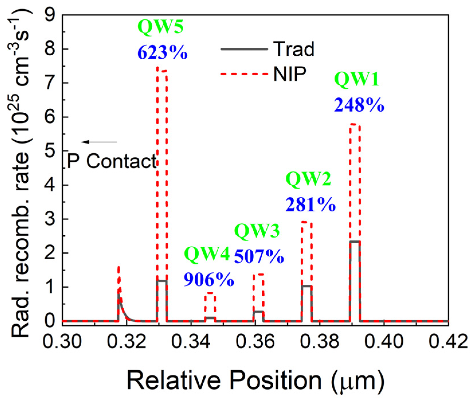
3.5. Radiative Recombination Rates

Figure 8 presents the carrier radiative recombination rate of the two LEDs, which helps identify the confinement of carriers within the active region caused by the inclusion of a last GaN barrier layer with an n-i-p configuration. Compared to the traditional LED, the radiative recombination rates of our proposed LED were increased to 623%, 906%, 507%, 281%, and 248% in QW5, QW4, QW3, QW2, and QW1, respectively, at a current injection density of 40 A/cm2. When a significant quantity of holes, each containing an equivalent number of electrons, are introduced into the active region, the trapped carriers will experience accelerated recombination within the MQWs. This phenomenon is particularly evident in the final quantum well (QW5), which is located closer to the last n-i-p-type GaN barrier and AlGaN EBL. These findings align closely with the aforementioned results. We can infer that the carrier injection and transport in our proposed LED structure are effectively enhanced by the last barrier being n-i-p-type GaN, leading to an accelerated recombination process towards the final quantum well (QW5). It is noteworthy that, while the increase in radiative recombination rate in QW4 is the highest, it constitutes a relatively minor proportion compared to the final quantum well (QW5) in terms of the overall radiative recombination. Consequently, the final quantum well (QW5) exerts the most significant influence.

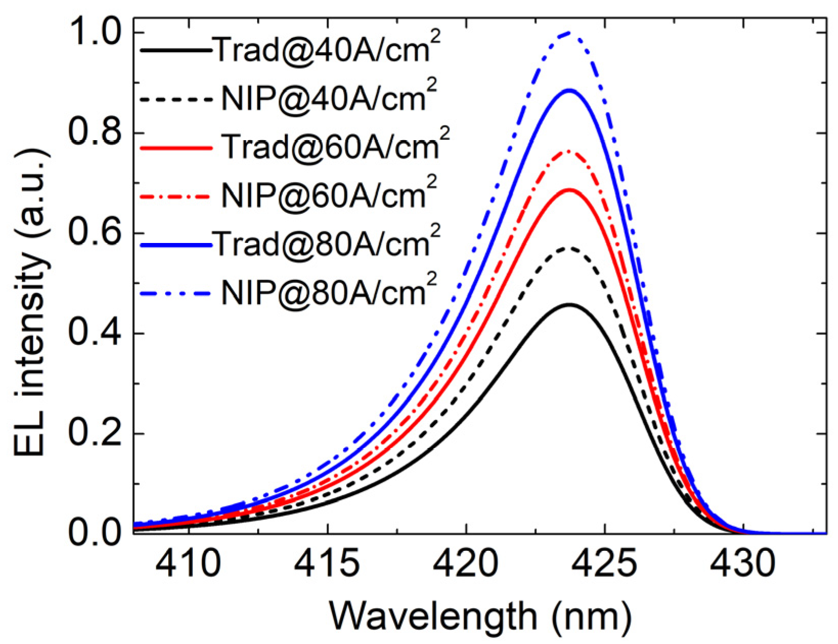
3.6. Electroluminescence Spectra

The calculated electroluminescence (EL) spectra for both devices at current densities of 40 A/cm2, 60 A/cm2, and 80 A/cm2 are depicted in Figure 9. A stronger EL intensity is observed for the LED with an n-i-p GaN barrier than for the LED with a traditional GaN barrier under all three current injection density conditions. In contrast to the conventional LED, the maximum intensities of our new structure LED rise to 124.6%, 111.6%, and 113.1% at current injection densities of 40 A/cm2, 40 A/cm2, and 40 A/cm2, respectively. The enhanced EL intensity can be attributed to the enhanced carrier transport across the GaN barrier in the n-i-p structure.

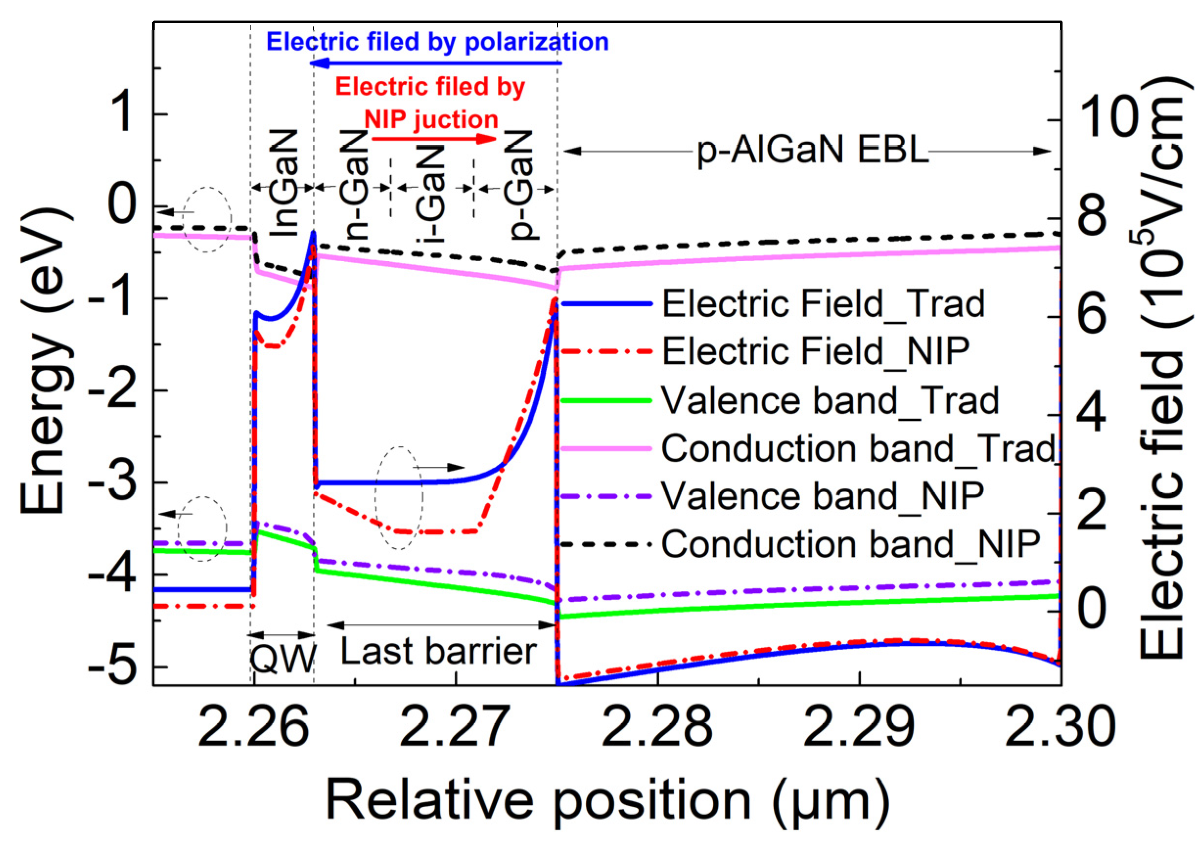
3.7. Electric Fields

In order to understand the underlying mechanism of carrier concentration distributions, it is necessary to analyze the electrostatic field in the final GaN barrier and the AlGaN EBL within these LED structures. The zoomed-in electric fields and energy band diagrams of the LEDs with an n-i-p GaN barrier and a traditional barrier at 40 A/cm2 are depicted in Figure 10. The energy band at the last GaN barrier and AlGaN EBL interface undergoes a downward shift due to the influence of polarization effect, resulting from the presence of strong electric fields in conventional LEDs. This leads to an increase in the effective barrier height for hole injection and a decrease in that for electron injection, which may contribute to the less-than-optimal efficiency of hole injection and the noticeable electron leakage observed in GaN-based MQW LEDs. However, the downward band bending at the interface between the last barrier and AlGaN EBL is significantly reduced as a result of the opposing electric field generated by the n-i-p junction in the GaN layers of the final barrier. It is evident that the barrier height experienced by holes is decreased while that for electrons is enhanced, which improves the hole injection efficiency and suppresses the electron leakage. In summary, the above results indicate that the introduction of an n-i-p GaN barrier can dramatically improve the GaN-based LED’s performance.

4. Conclusions

In summary, a comprehensive numerical analysis and comparison have been conducted on two distinct categories of GaN-based LEDs. One is an LED with a traditional GaN barrier for the last quantum well, and the other is an LED with our newly proposed n-i-p GaN barrier for the last quantum well. The light output power of the LED with the n-i-p GaN last quantum barrier is significantly improved by 105% when exposed to an injection current density of 100 A/cm2. Our research findings suggest that, by employing an n-i-p GaN barrier as the final quantum well, it is possible to enhance hole injection efficiency from the p-type GaN cap region into the active regions and effectively mitigate electron leakage from the active regions. Therefore, the carrier confinement within the active regions is improved. As a result, our newly devised barrier design exhibits remarkable enhancements in various aspects such as increased light output power, reduced turn-on voltage, and intensified EL emission intensity. The results obtained in this study present a novel approach for enhancing the efficiency of GaN-based LEDs. The suggested design can be easily implemented during the fabrication process of LEDs, eliminating any challenges associated with lattice mismatching that may arise during additional heterostructure growth.

Author Contributions

Conceptualization, J.W. and Z.X.; methodology, J.W.; software, J.W.; validation, J.W. and Y.X.; formal analysis, J.W and Y.X.; investigation, J.W and Y.X.; resources, J.W. and Z.X.; data curation, J.W. and X.W.; writing—original draft preparation, J.W. and X.W.; writing—review and editing, X.W. and Z.X.; visualization, Y.X.; supervision, J.W.; project administration, M.G.; funding acquisition, J.W. All authors have read and agreed to the published version of the manuscript.

Funding

This work was supported in part by the Anhui Provincial Natural Science Foundation (No. 2108085MF228), Hefei Municipal Natural Science Foundation (No. 2021002), National Key Research and Development Program of China (No. 2017YFA0402904, No. 2018YFB2200204, No. 2018YFB2200205).

Data Availability Statement

The data that support the findings of this study are available from the corresponding author upon reasonable request.

Conflicts of Interest

The authors declare no conflicts of interest.

References

  1. Liu, Y.; Xia, T.; Du, A.; Liang, T.; Fan, Z.; Chen, E.; Sun, J.; Yan, Q.; Guo, T. Omnidirectional color shift suppression of full-color micro-LED displays with enhanced light extraction efficiency. Opt. Lett. 2023, 48, 1650–1653. [Google Scholar] [CrossRef]
  2. Zhao, J.; Chen, K.; Gong, M.G.; Hu, W.X.; Liu, B.; Tao, T.; Yan, Y.; Xie, Z.L.; Li, Y.Y.; Chang, J.H. Epitaxial Growth and Characteristics of Nonpolar a-Plane InGaN Films with Blue-Green-Red Emission and Entire In Content Range. Chin. Phys. Lett. 2022, 39, 048101. [Google Scholar]
  3. Zhuang, Z.; Iida, D.; Ohkawa, K. Investigation of InGaN-based red/green micro-light-emitting diodes. Opt. Lett. 2021, 46, 1912–1915. [Google Scholar] [CrossRef] [PubMed]
  4. Zhang, Y.Y.; Yin, Y.A. Performance enhancement of blue light emitting diodes with a special designed AlGaN/GaN supperlattice electron- blocking layer. Appl. Phys. Lett. 2011, 99, 221103. [Google Scholar] [CrossRef]
  5. Schubert, E.F. Light-Emitting Diodes, 2nd ed.; Cambridge University Press: Cambridge, UK, 2006. [Google Scholar]
  6. Wang, F.; Li, S.-S.; Xia, J.-B.; Jiang, H.X.; Lin, J.Y.; Li, J.; Wei, S.-H. Effects of the wave function localization in AlInGaN quaternary alloys. Appl. Phys. Lett. 2007, 91, 061125. [Google Scholar] [CrossRef]
  7. Aumer, M.E.; LeBoeuf, S.F.; McIntosh, F.G.; Bedair, S.M. High optical quality AlInGaN by metalorganic chemical vapor deposition. Appl. Phys. Lett. 1999, 75, 3315–3317. [Google Scholar] [CrossRef]
  8. Kuo, Y.K.; Tsai, M.C.; Yen, S.H. Numerical simulation of blue InGaN light-emitting diodes with polarization-matched AlGaInN electron-blocking layer and barrier layer. Opt. Commun. 2009, 282, 4252–4255. [Google Scholar] [CrossRef]
  9. Lin, Z.; Wang, H.; Chen, S.; Lin, Y.; Yang, M.; Li, G.; Xu, B. Achieving High-Performance Blue GaN-Based Light-Emitting Diodes by Energy Band Modification on AlxInyGa1−x−yN Electron Blocking Layer. IEEE Trans. Electron Devices 2017, 64, 472–480. [Google Scholar] [CrossRef]
  10. Gu, W.; Lu, Y.; Lin, R.; Guo, W.; Zhang, Z.-H.; Ryou, J.-H.; Yan, J.; Wang, J.; Li, J.; Li, X. BAlN for III-nitride UV light-emitting diodes: Undoped electron blocking layer. J. Phys. D Appl. Phys. 2021, 54, 175104. [Google Scholar] [CrossRef]
  11. Xing, Z.; Wang, F.; Wang, Y.; Liou, J.J.; Liu, Y. Enhanced performance in deep-ultraviolet laser diodes with an undoped BGaN electron blocking layer. Opt. Express 2022, 30, 36446–36455. [Google Scholar] [CrossRef]
  12. Yang, G.; Tong, Y.; Xie, F.; Yan, D.; Wang, F. Design analysis of polarization-doped N-face InGaN/GaN light-emitting diodes with different AlxGa1−xN graded layers. Mater. Sci. Semicond. Process. 2015, 29, 362–366. [Google Scholar] [CrossRef]
  13. Usman, M.; Munsif, M.; Anwar, A.R.; Malik, S.; Islam, N.U.; Khan, S. Hole transport enhancement by thickness- and composition-grading of electron blocking layer. Opt. Eng. 2021, 60, 036101. [Google Scholar] [CrossRef]
  14. Xia, C.S.; Simon Li, Z.M.; Li, Z.Q.; Sheng, Y. Effect of multiquantum barriers in performance enhancement of GaN-based light-emitting diodes. Appl. Phys. Lett. 2013, 102, 013507. [Google Scholar]
  15. Xing, Z.; Wang, Y.; Wang, F.; Liou, J.J.; Liu, Y. Improvement of the optoelectronic characteristics in deep-ultraviolet laser diodes with tapered p-cladding layer and triangular electron blocking layer. Appl. Phys. B 2022, 128, 197. [Google Scholar] [CrossRef]
  16. Tian, W.; Liu, M.; Li, S.; Liu, C. Improving the hole injection efficiency in AlGaN DUV LEDs by minimizing the band offset at the p-EBL/hole supplier interface. Opt. Mater. Express 2023, 13, 2449–2459. [Google Scholar] [CrossRef]
  17. Xia, C.S.; Simon Li, Z.M.; Lu, W.; Zhang, Z.H.; Sheng, Y.; Cheng, L.W. Droop improvement in blue InGaN/GaN multiple quantum well light-emitting diodes. Appl. Phys. Lett. 2011, 99, 233501. [Google Scholar]
  18. Lin, B.-C.; Chen, K.-J.; Wang, C.-H.; Chiu, C.-H.; Lan, Y.-P.; Lin, C.-C.; Lee, P.-T.; Shih, M.-H.; Kuo, Y.-K.; Kuo, H.-C. Hole injection and electron overflow improvement in InGaN/GaN light-emitting diodes by a tapered AlGaN electron blocking layer. Opt. Express 2014, 22, 463–469. [Google Scholar] [CrossRef] [PubMed]
  19. Zhang, Z.-H.; Kyaw, Z.; Liu, W.; Ji, Y.; Wang, L.; Tan, S.T.; Sun, X.W.; Demir, H.V. A hole modulator for InGaN/GaN light-emitting diodes. Appl. Phys. Lett. 2015, 106, 063501. [Google Scholar] [CrossRef]
  20. Bao, X.; Sun, P.; Liu, S.; Ye, C. Performance Improvements for AlGaN-Based Deep Ultraviolet Light-Emitting Diodes With the p-Type and Thickened Last Quantum Barrier. IEEE Photonics J. 2015, 7, 1400110. [Google Scholar] [CrossRef]
  21. Chu, C.; Tian, K.; Che, J.; Shao, H.; Kou, J.; Zhang, Y.; Li, Y.; Wang, M.; Zhu, Y.; Zhang, Z.H. On the origin of enhanced hole injection for AlGaN-based deep ultraviolet light-emitting diodes with AlN insertion layer in p-electron blocking layer. Opt. Exp. 2019, 27, 620–628. [Google Scholar] [CrossRef]
  22. Wang, L.-Y.; Song, W.-D.; Hu, W.-X.; Li, G.; Luo, X.-J.; Wang, H.; Xiao, J.-K.; Guo, J.-Q.; Wang, X.-F.; Hao, R.; et al. Efficiency enhancement of ultraviolet light-emitting diodes with segmentally graded p-type AlGaN layer. Chin. Phys. B 2019, 28, 018503. [Google Scholar] [CrossRef]
  23. Liu, Z.; Yu, H.; Ren, Z.; Dai, J.; Chen, C.; Sun, H. Polarization-engineered AlGaN last quantum barrier for efficient deep-ultraviolet light-emitting diodes. Semicond. Sci. Technol. 2020, 35, 075021. [Google Scholar] [CrossRef]
  24. Wu, J.; Li, P.; Zhou, X.; Wu, J.; Hao, Y. Increasing the Carrier Injection Efficiency of GaN-Based Ultraviolet Light-Emitting Diodes by Double Al Composition Gradient Last Quantum Barrier and p-Type Hole Supply Layer. IEEE Photonics J. 2021, 13, 1–8. [Google Scholar] [CrossRef]
  25. Liu, M.; Liu, C. Enhanced Carrier Injection in AlGaN-Based Deep Ultraviolet Light-Emitting Diodes by Polarization Engineering at the LQB/p-EBL Interface. IEEE Photonics J. 2022, 14, 8228005. [Google Scholar] [CrossRef]
  26. Khan, M.A.; Matsuura, E.; Kashima, Y.; Hirayama, H. Influence of Undoped-AlGaN Final Barrier of MQWs on the Performance of Lateral-Type UVB LEDs. Phys. Status Solidi 2019, 216, 1900185. [Google Scholar] [CrossRef]
  27. Memon, M.H.; Yu, H.; Jia, H.; Xiao, S.; Wang, R.; Sun, H. Last-Quantum-Barrier-Free AlGaN Deep Ultraviolet LEDs With Boosted Efficiency. IEEE Trans. Electron Devices 2023, 70, 5151–5155. [Google Scholar] [CrossRef]
  28. Hu, Y.; Wang, J.; Guo, J. Efficiency Enhancement of GaN Based Light-Emitting Diodes with a Heterojunction Type Last Quantum Barrier. In Proceedings of the International Conference on Informatics, Shanghai, China, 2–4 November 2019. [Google Scholar]
  29. Zhang, Z.-H.; Zhang, Y.; Bi, W.; Geng, C.; Xu, S.; Demir, H.V.; Sun, X.W. On the hole accelerator for III-nitride light-emitting diodes. Appl. Phys. Lett. 2016, 108, 151105. [Google Scholar] [CrossRef]
  30. Chuang, S.L.; Chang, C.S. A Band-Structure Model of Strained Quantum-Well Wurtzite Semiconductors. Semicond. Sci. Technol. 1997, 12, 252. [Google Scholar] [CrossRef]
  31. Wang, X.; Jiang, K.; Sun, Z.; Zhang, Z.-H.; Chen, Y.; Wang, B.; Li, D. Valence subbands profile regulation in AlGaN quantum well based on k·p theory. Phys. Scr. 2023, 98, 035103. [Google Scholar] [CrossRef]
  32. Piprek, J. Semiconductor Optoelectronic Devices: Introduction to Physics and Simulation; Academic Press: Cambridge, MA, USA; UCSB: Santa Barbara, CA, USA, 2003; 22. [Google Scholar]
  33. Wang, K.; Lian, C.; Su, N.; Jena, D.; Timler, J. Conduction band offset at the InN/GaN heterojunction. Appl. Phys. Lett. 2007, 91, 232117. [Google Scholar] [CrossRef]
  34. Verzellesi, G.; Saguatti, D.; Meneghini, M.; Bertazzi, F.; Goano, M.; Meneghesso, G.; Zanoni, E. Efficiency droop in InGaN/GaN blue light-emitting diodes: Physical mechanisms and remedies. J. Appl. Phys. 2013, 114, 071101. [Google Scholar] [CrossRef]
  35. Ambacher, O.; Smart, J.; Shealy, J.R.; Weimann, N.G.; Chu, K.; Murphy, M.; Schaff, W.J.; Eastman, L.F.; Dimitrov, R.; Wittmer, L.; et al. Two Dimensional Electron Gases Induced by Spontaneous and Piezoelectric Polarization in Undoped and Doped AlGaN/GaN Heterosturctures. J. Appl. Phys. 2000, 87, 334–344. [Google Scholar] [CrossRef]
  36. Fiorentini, V.; Bernardini, F.; Ambacher, O. Evidence for nonlinear macroscopic polarization in III–V nitride alloy heterostructures. Appl. Phys. Lett. 2002, 80, 1204–1206. [Google Scholar] [CrossRef]
  37. Ridley, B.K.; Schaff, W.J.; Eastman, L.F. Theoretical model for polarization superlattices: Energy levels and intersubband transitions. J. Appl. Phys. 2003, 94, 3972–3978. [Google Scholar] [CrossRef]
  38. Bernardini, F.; Fiorentini, V.; Vanderbilt, D. Accurate calculation of polarization-related quantities in semiconductors. Phys. Rev. B 2001, 63, 193201. [Google Scholar] [CrossRef]
Figure 1. Schematic diagrams depicting the LEDs with (a) a traditional GaN barrier and (b) an n-i-p GaN barrier for the last quantum well.
Electronics 13 01399 g001
Figure 2. Simulated and experimentally measured optical power of a reference InGaN/GaN LED as a function of injection current.
Electronics 13 01399 g002
Figure 3. Light output power for the LEDs with a traditional GaN barrier and with an n-i-p GaN barrier for the last quantum well.
Electronics 13 01399 g003
Figure 4. Energy band diagrams of the LEDs with a traditional GaN barrier (a) and with an n-i-p barrier GaN (b) at 40 A/cm2.
Electronics 13 01399 g004aElectronics 13 01399 g004b
Figure 5. The calculated hole and electron concentrations of the LEDs with a traditional GaN barrier and with an n-i-p GaN barrier at a current density of 40 A/cm2.
Electronics 13 01399 g005
Figure 6. Simulated electron and hole current density profiles of the LEDs at 40 A/cm2 with and without the last n-i-p GaN barrier.
Electronics 13 01399 g006
Figure 7. I–V curves for the LEDs with a traditional GaN barrier and with an n-i-p GaN barrier for the last quantum well.
Electronics 13 01399 g007
Figure 8. Carrier relative radiative recombination rate at a current density of 40 A/cm2.
Electronics 13 01399 g008
Figure 9. Simulated EL spectra for the LEDs with a traditional GaN barrier and with an n-i-p GaN barrier for the last QW at a current density of 40 A/cm2,60 A/cm2, and 80 A/cm2, respectively.
Electronics 13 01399 g009
Figure 10. Zoomed-in energy band diagrams and electric fields of the LEDs with an n-i-p GaN barrier and a traditional barrier at a current density equivalent to 40 A/cm2.
Electronics 13 01399 g010
Disclaimer/Publisher’s Note: The statements, opinions and data contained in all publications are solely those of the individual author(s) and contributor(s) and not of MDPI and/or the editor(s). MDPI and/or the editor(s) disclaim responsibility for any injury to people or property resulting from any ideas, methods, instructions or products referred to in the content.

