Abstract
This paper proposes a VCO-based ADC with first-order noise shaping for EEG signal recording front ends. Addressing the challenge of applying analog integrators in advanced processes due to low voltage issues, a multi-phase quantizer structure is introduced based on V-F conversion within the VCO structure, resulting in lower analog power consumption at the same output bit-width. By introducing a form of Gray code encoding, errors caused by circuit metastability are limited to within 1 bit. Considering the effects of motion artifacts and the electrode DC offset, the circuit achieves a wide input range of 500 m by adjusting the feedback coefficients. A prototype ADC is fabricated using 180 nm CMOS technology, operating at a 1.8 V/1 V power supply voltage, with power consumption of 17.1 W, while achieving a 62.1 dB signal-to-noise and distortion ratio (SNDR) and 55.2 dB dynamic range (DR). The proposed ADC exhibits input noise of 8.64 within a bandwidth of 0.5 Hz–5 kHz.
1. Introduction
In modern clinical practice, EEG signals are obtained by measuring the scalp electrical potential at multiple locations on the head to reflect the spontaneous electrical activity in the brain [1]. Meanwhile, scalp EEG measurement, as a non-invasive method, has played an important role in measuring and assessing brain diseases, including epileptic seizures and Alzheimer’s disease, as well as sleep disorders [2]. In brain–computer interface (BCI) systems, EEG recording circuits capture information about the brain by capturing the strength and spatial distribution of the electrical potentials at different locations in the brain. Compared to invasive methods, which carry the risk of trauma, non-invasive EEG recording circuits face greater challenges due to the electrode DC offset (EDO) and motion artifacts (MA), which can affect the accuracy of the recordings [3].
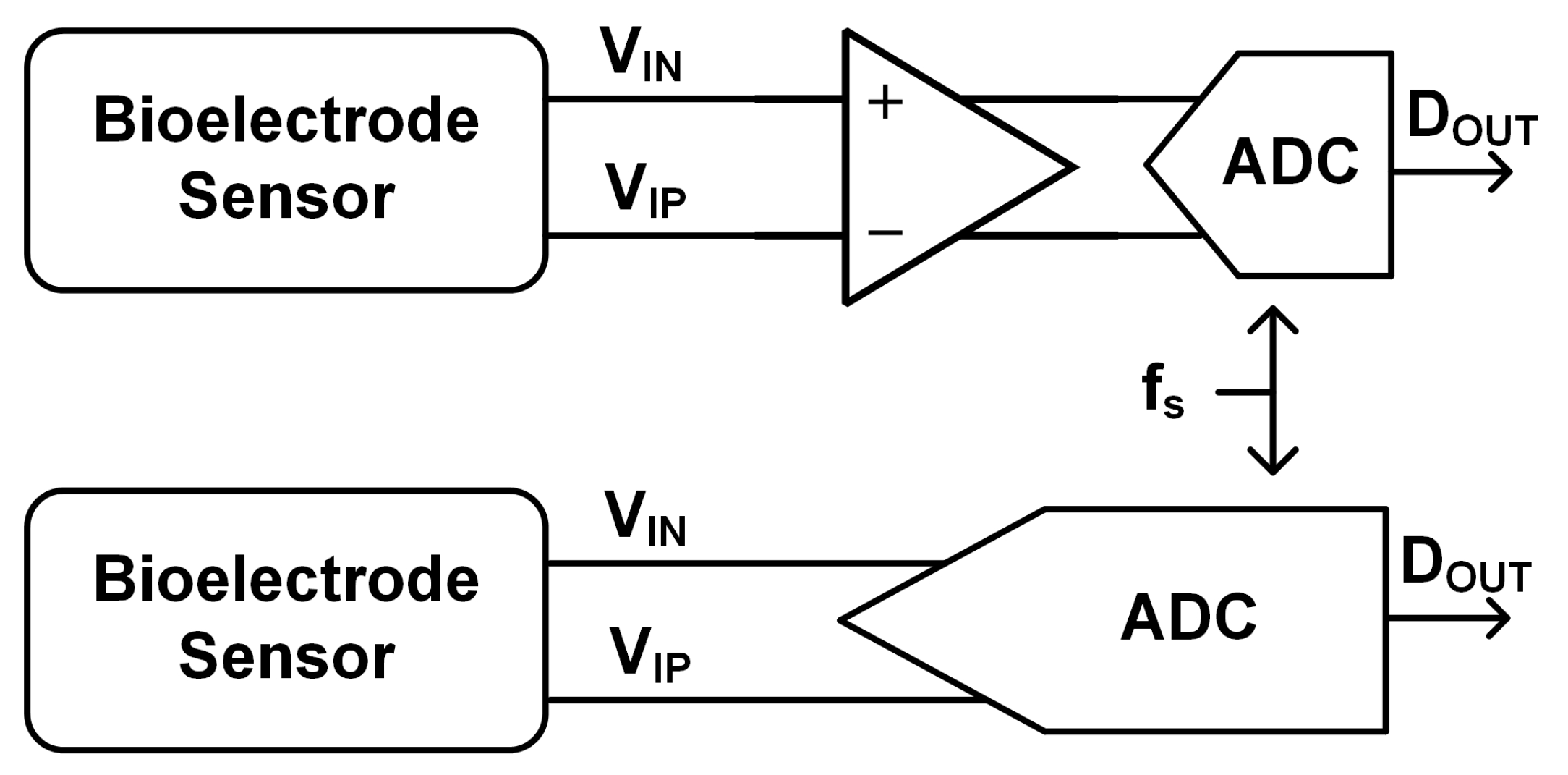
Currently, there are two main approaches to non-invasive EEG recording circuits. In one, each channel is composed of a low-noise instrumentation amplifier (IA) and a medium-accuracy analog-to-digital converter (ADC) [3,4,5,6,7,8,9,10,11,12,13], as shown in Figure 1. This method can obtain relatively low input reference noise (IRN) and superior common mode rejection ratio (CMRR) performance. However, MA and EDO on the mV scale tend to saturate the front-end amplifier, limiting the gain of the front-end amplifier. To reduce the impact of EDO, amplifiers usually require large external capacitors or additional DC servo loops (DSL) [14,15,16]. This approach increases the chip area and power consumption and limits the miniaturization of EEG recording circuits. Another approach is to use the ADC direct structure [17,18,19,20], combine the IA and ADC functions, and directly digitize the input EEG signals. This is commonly achieved using discrete-time (DT) or continuous-time (CT) ADC architectures, allowing for a relatively high signal-to-noise and distortion ratio (SNDR). However, this structure faces challenges due to its heavy reliance on voltage-domain-based integrators and comparators, which are sensitive to process scaling. Additionally, suppressing kT/c noise in DT structures or maintaining the linearity of the -C filter in CT structures is often required [21].

Figure 1.
The implementation method of an EEG recording circuit.
To overcome the limitations of traditional voltage domain processing in advanced technology nodes, the EEG recording circuit topology based on a voltage-controlled oscillator (VCO) directly converts the input voltage to the frequency domain, thus avoiding the constraints imposed by the power supply voltage [22,23,24,25,26]. The frequency output of the VCO is quantized by measuring the phase increment over a specific time window. At the same time, VCO-based circuits do not need to stack transistors like traditional analog amplifiers to achieve unlimited DC gain. Although the VCO-based structure offers a high level of digitization, the analog components, particularly the VCO circuit, still account for a significant portion of the overall circuit’s power consumption.
This paper proposes a digital circuit structure with multiple quantizers, which reduces the center frequency of the VCO in the analog circuit to 1/2 N, achieving a significant reduction in the power consumption of the analog VCO circuit with the same output bit resolution. By introducing a form of Gray code encoding, the errors caused by circuit metastability are limited to within 1 bit. By adjusting the feedback coefficients to constrain the residual signal to within 10 mV, the circuit achieves a wide input range of 500 m. The overall circuit is highly digitized, and a first-order noise shaping effect is achieved using digital differential circuits.
This paper provides a comprehensive description of the architecture and theory of the circuit, as well as the details of its implementation and measurement. The content is structured as follows. Section 2 provides a detailed description of the principle analysis and implementation status of the proposed circuit. Section 3 introduces the measurement results and analysis and compares the performance with other works. Finally, Section 4 concludes the paper.
2. Circuit Design
2.1. V/I Conversion Circuit
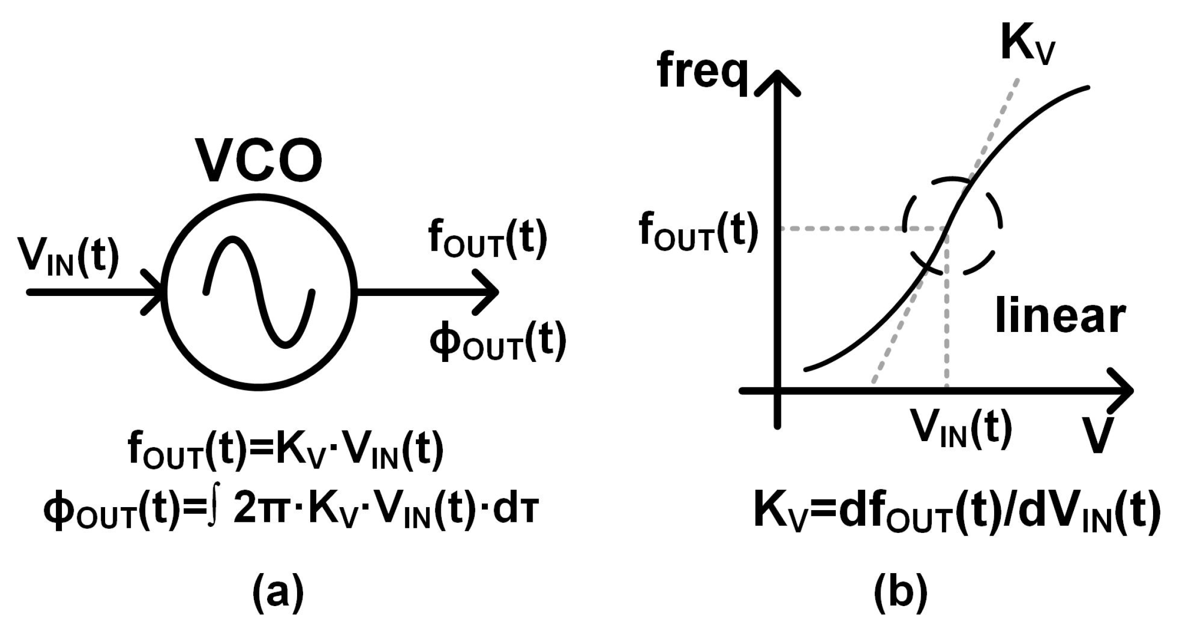
The VCO can convert the input analog voltage into a corresponding frequency or phase signal, as shown in Figure 2. The mathematical model is equivalent to a CT voltage phase integrator with an infinite DC gain. In the specific circuit implementation, a VCO-based ADC can be achieved with a combination of digital circuits and simple analog circuits. It replaces the traditional, predominantly analog integrators and comparators, performing integration and quantization in the phase or frequency domain. Despite the high scalability of VCO-based ADC structures, the nonlinearity introduced during the V-F conversion process by the VCO is one of the key factors affecting the performance.

Figure 2.
(a) VCO conversion. (b) Nonlinearity of the VCO.
For a current-starved VCO composed of N stages of inverters, its can be expressed as follows:
where C represents the parasitic capacitance of the VCO composed of inverters, which is associated with the WL of the inverter. denotes the output voltage swing of the current-starved VCO. denotes the transconductance of the input V/I circuit. is not a linear quantity. As the input voltage varies, the state of the MOS transistor changes. There are two methods to improve the linearity of the transconductance . The first method involves operating the entire circuit in a closed loop, adjusting the feedback coefficient, and controlling the ratio of to to reduce the amplitude of the summed input to several millivolts. The second method is to improve the linearity of the V/I circuit.
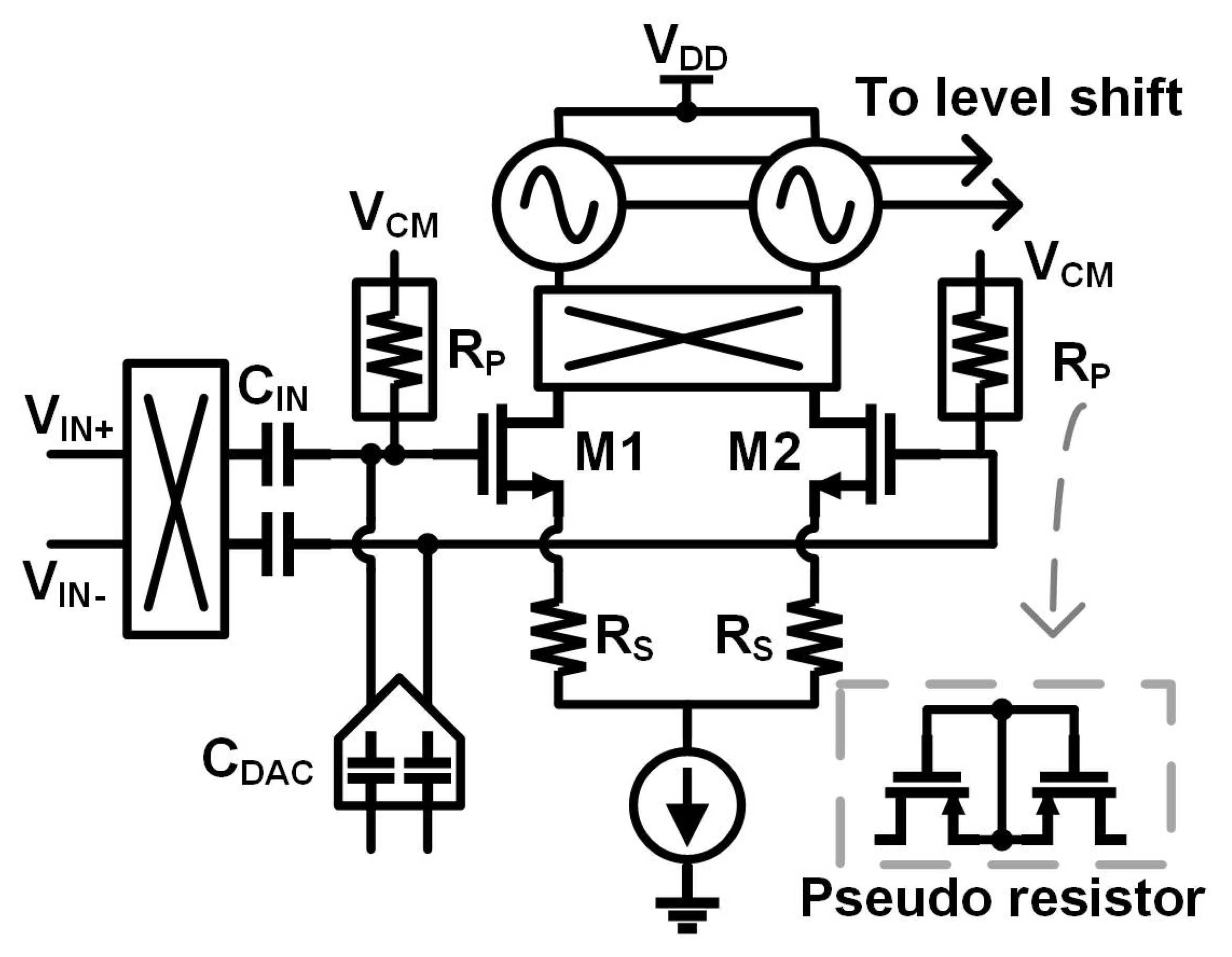
As shown in Figure 3, the VCO-based ADC front end consists of a V/I converter composed of differential pairs M1 and M2 and a set of current-starved voltage-controlled oscillators (CCOs). To enhance the linearity of the differential pairs, a source degeneration structure with a resistor is employed, resulting in the following gain of the V/I converter:

Figure 3.
Schematic diagram of V/I conversion circuit.
The linearity of the V/I conversion is enhanced by employing the source degeneration structure. To achieve current multiplexing and improve the current efficiency, the V/I conversion circuit is stacked with 16 pairs of CCOs. The frequency range of the EEG signal distribution is typically 0.5–100 Hz, which requires the high-pass filter (HPF) cutoff frequency composed of the input capacitor and the bias resistor to be below 0.5 Hz. To achieve resistance of tens of G, the input of the V/I conversion is biased by a pseudo-resistance composed of an MOS transistor. The amplitude of the summed input at the input terminal of the V/I circuit is kept within 10 mV by adjusting the feedback coefficient. This approach not only ensures that the MOS transistors remain in saturation but also minimizes the input swing, thereby maintaining the pseudo-resistor at a high level and effectively reducing the impact of noise originating from the pseudo-resistor. To avoid a gate leakage current, thick oxide transistors are used for the differential pairs M1 and M2. Furthermore, chopper techniques are used to reduce the IRN.
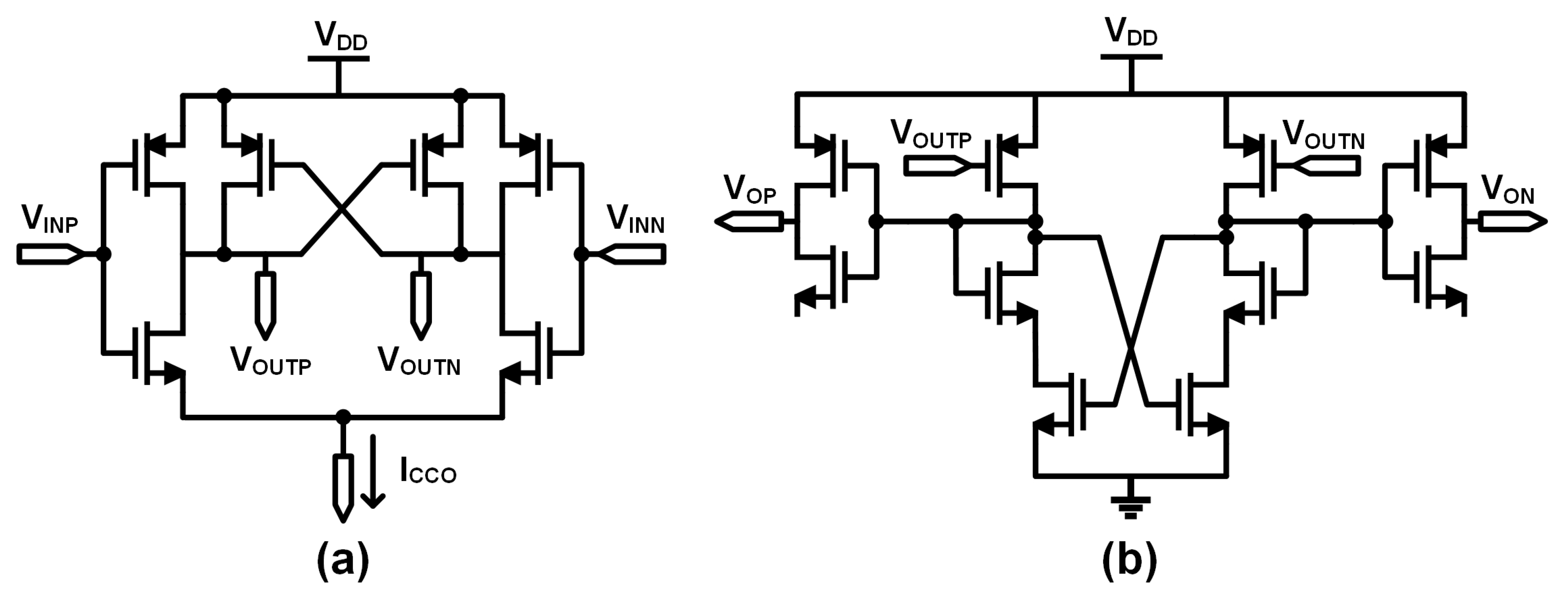
Figure 4a shows the implementation of the CCO circuit, where each delay cell comprises an inverter pair and two cross-coupled PMOS transistors, effectively reducing flicker noise. Regarding the phase noise of VCO, it is negligible when equivalent to the input. Due to the CCOs being stacked on the differential pair, the output waveform amplitude remains relatively small. Therefore, a level shifter is required to achieve a rail-to-rail output waveform, as shown in Figure 4b.
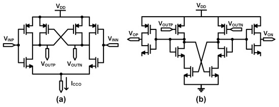
Figure 4.
(a) Delay cell circuit. (b) Level shift circuit.
2.2. Basic Linear Model
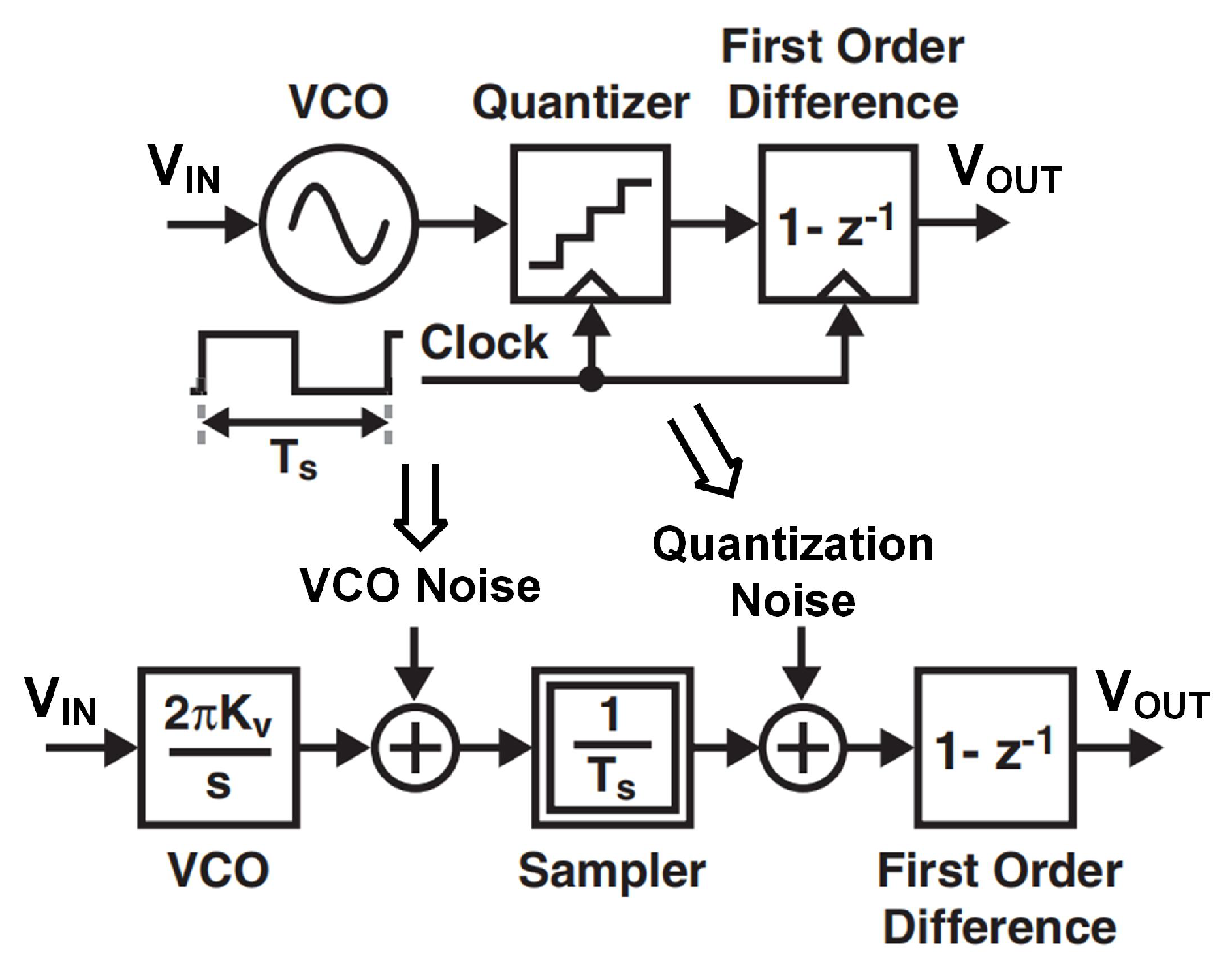
Firstly, an analysis of the first-order linear model for a VCO-based ADC is conducted. In Figure 5, the upper part is the functional block diagram of a VCO quantizer, while the lower part corresponds to its linearized frequency domain model. The VCO module, corresponding to the VI and CCO, performs voltage-to-current and current-to-frequency conversions on the input VIN signal, respectively. The quantizer module, represented by a set of registers, is responsible for sampling and quantizing the phase signal output from the VCO.
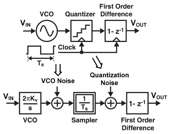
Figure 5.
Block diagram model and corresponding linearized frequency domain model of VCO-based quantizer.
In the corresponding frequency domain model, the VCO module is represented as an integrator with a gain of 2, tasked with converting the input signal into the VCO’s phase signal, introducing a certain amount of phase noise in the process. The quantizer is depicted as a sampling circuit with a specific sampling time, where quantization noise is introduced into the circuit. For ease of understanding, the first-order differencing module is represented as a discrete-time differentiator performing the transfer function 1 − .
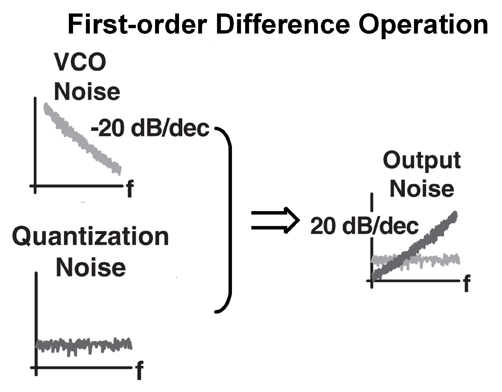
As shown in Figure 6, the quantization noise first undergoes first-order noise shaping through the differencing operation depicted in the diagram. It is also observable that the VCO’s phase noise undergoes shaping. However, due to the original phase noise signal possessing a slope of −20 dB/dec, the result of the shaping is a flat spectrum. In practical scenarios, the shaped VCO phase noise would also contain 1/f noise, but, for the sake of the following analysis, this aspect is temporarily simplified.
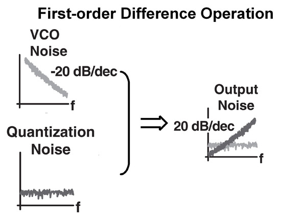
Figure 6.
Noise shaping of linearized frequency domain models.
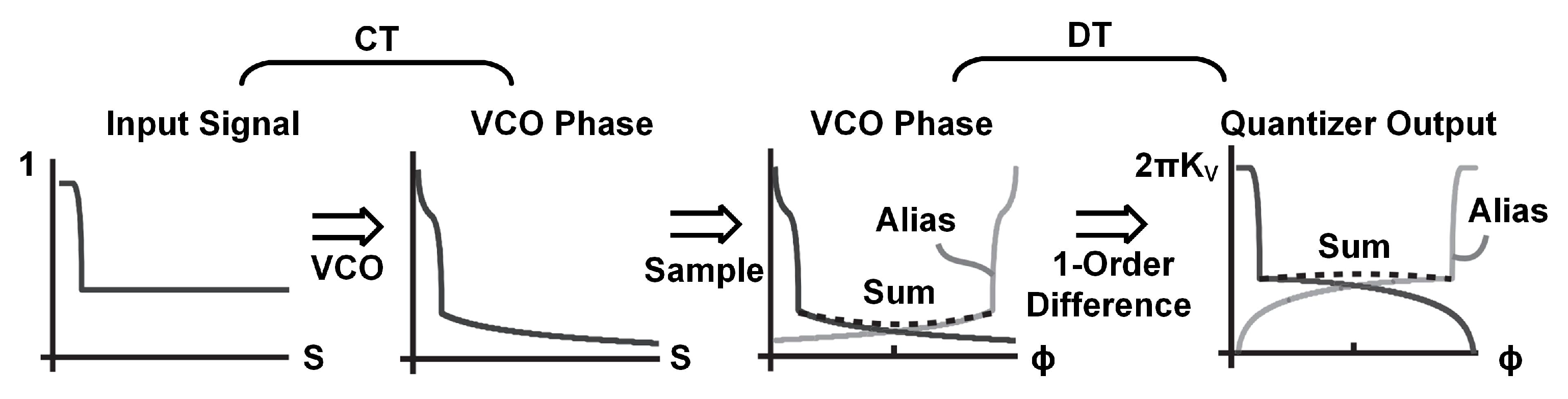
In fact, the first-order differencing module transforms the VCO phase signal into the corresponding VCO frequency signal. However, discrete-time (DT) differentiation is not the exact inverse of continuous-time (CT) integration. Firstly, sampling introduces aliasing in the input signal, and the 1 − filter only serves as an approximation of CT differentiation. As depicted in Figure 7, the resulting DT spectrum of the VCO frequency measurement closely follows the input spectrum at low frequencies and possesses a low-frequency gain factor of 2. However, as the frequency approaches /2 ( = ), the spectrum begins to slightly drop due to the CT/DT inversion approximation.
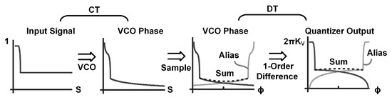
Figure 7.
Spectrogram based on VCO quantization.
By comparing the reconstructed input signal (in dark lines) with a copy of the aliased signal (in lighter lines) through the output of the VCO quantizer, it can be observed that the VCO-based quantizer inherently functions as a first-order anti-aliasing filter. Although the structure of this first-order anti-aliasing filter is simple, its effectiveness in suppressing the aliased signal is roughly equivalent to 20 log (/).
For linear analysis, it is necessary to select a primary time domain for the corresponding calculations. Typically, modeling and analysis in the DT domain are already quite mature. Therefore, it is required to convert models operating in the CT domain into their respective DT domain models.
Firstly, CT integration can be approximated as a DT accumulator by using the Taylor series expansion of the exponential function .
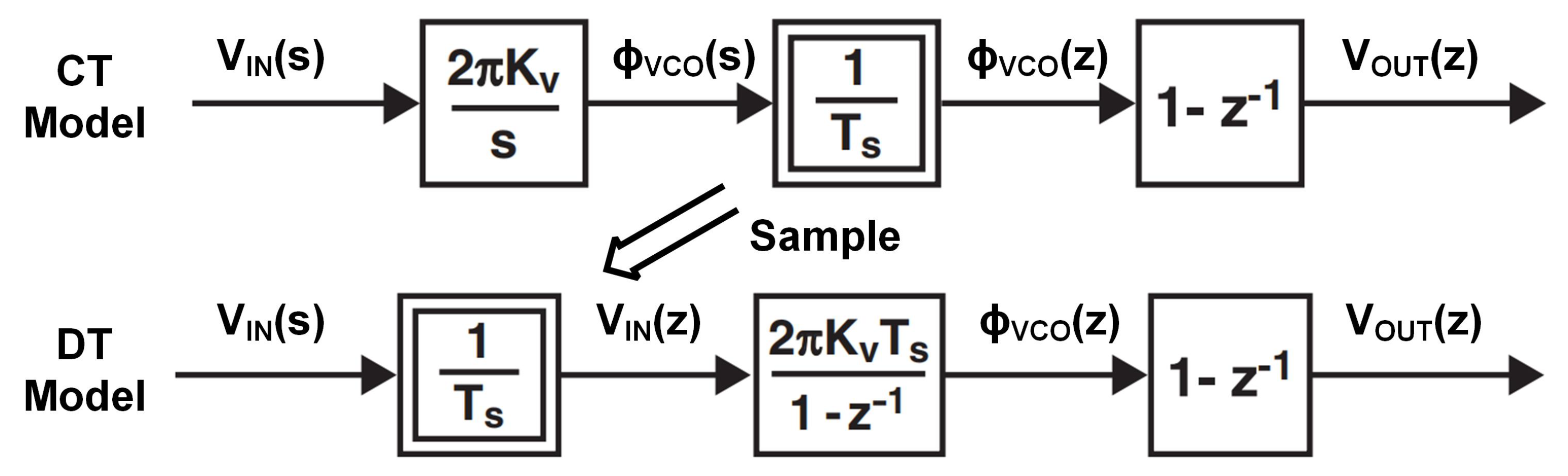
To construct the DT model, first replace the gain of the CT-VCO, 2/s, with the gain formula for the DT-VCO, 2/(1 − , and move the gain of the sampler, 1/, in front of the VCO quantizer, as shown in Figure 8. For low-frequency input signals, the VCO quantizer is approximated as a single module with a gain (z), which converts the input voltage (z) into the frequency at VCO output (z):
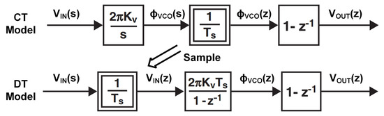
Figure 8.
The conversion of the CT linear model and DT linear model.
Combining the expression for given in Equation (1), the expression for the signal-to-quantization-noise ratio (SQNR) can be derived as follows [12]:
where A is the amplitude of the input sinusoidal signal, and represents the signal bandwidth. It can be observed from Equation (5) that the size of the SQNR is related to the delay and swing of the VCO. With the continuous advancement of technology, both the parasitic capacitance C and of the VCO can be reduced, thereby increasing the SQNR. This demonstrates the advantages of VCO-based quantizers in advanced process technologies.
2.3. VCO-Based ADC Quantization Process
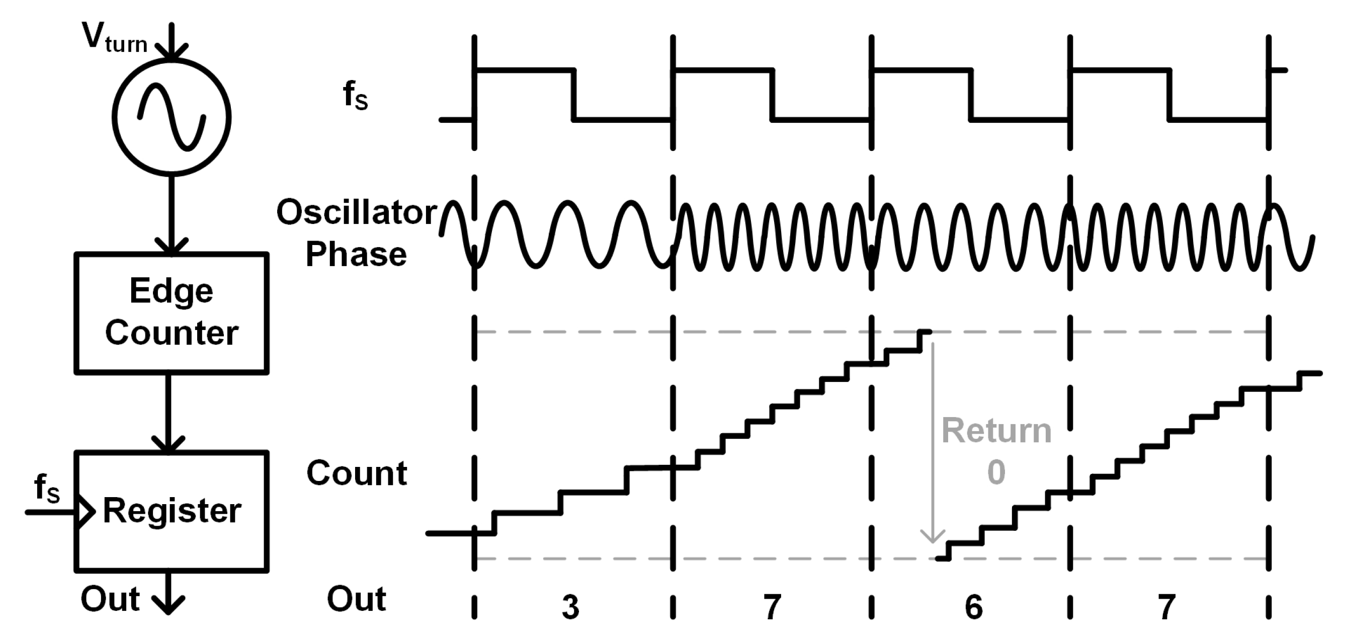
As shown in Figure 9, different input voltages result in varying oscillation frequencies in the VCO. The output waveform of the VCO is sampled by an edge counter after level shifting and stored in a set of registers (DFFs) at a sampling frequency . In this design, the edge counter operates in a cyclic manner without the need for resetting and provides the output as the difference between two consecutive register values. The purpose of this approach is to preserve the truncation error q[n] that occurs at the end of each clock cycle, allowing it to accumulate in the next cycle. If the accumulated quantization error exceeds one LSB, an additional output is generated. This ensures that the quantization error between samples remains within one LSB.

Figure 9.
Simplified VCO-based ADC quantization process.
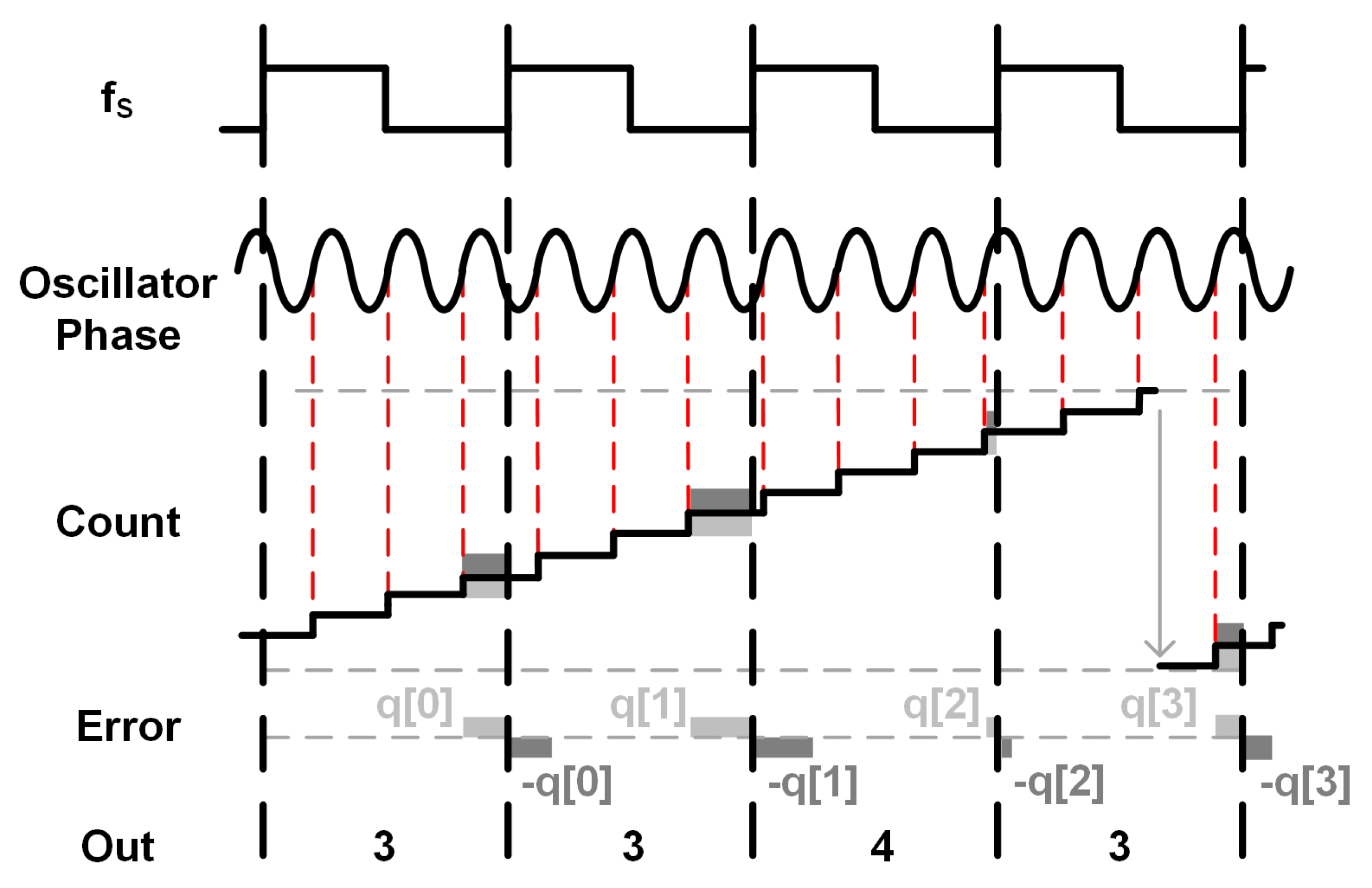
As shown in Figure 10, since the residual phase from the previous sampling period q[n] inherently becomes the initial phase for the next sampling period, when the quantization error of the third sample exceeds one LSB, the output sequence is [3 3 4 3]. At this point, the manifestation of the quantization error is as follows:
where q[n] corresponds to the truncation error that occurs between the edges of each clock cycle. The output of the VCO-quantizer can therefore be expressed as
where is the number of VCO phases and is the VCO phase change caused by the analog input . By applying the z-transform to the equation, we can obtain
Figure 10.
The principle of first-order noise shaping.
From Equation (8), it can be observed that the quantization error of the VCO quantizer is shaped by first-order noise shaping. Therefore, it is equivalent to a first-order Sigma-Delta modulator.
2.4. Multi-Phase Quantizer Circuit
The power consumption of the analog section in the circuit mainly originates from the oscillation of the VCO, where a higher oscillation frequency requires a larger current. To reduce the power consumption of the analog circuit and improve the original resolution, the VCO needs to generate more edge transitions during sampling. This design utilizes an edge counter that counts both rising and falling edges simultaneously. Assuming that the center frequency of the VCO is , in the case wherein the number of ADC output bits is determined, this design can reduce to half of its original value. Moreover, this design uses a multi-phase quantizer to quantify the output of the VCO. Assuming that the number of quantizers is N, this method can reduce to the original 1/N. By combining these two approaches, the center frequency of the VCO in the analog circuit can be decreased to /2 N, significantly reducing the current consumption of the analog circuit.
As shown in Figure 11, to balance the reduction in current consumption of the analog VCO and the increased power consumption of multiple phase quantizers, a simulation was conducted to obtain the relationship between the number of phase quantizers and the total power consumption of the chip. From the figure, it is evident that with an increase in the number of phase quantizers, there is a significant reduction in the power consumption of the analog VCO part. The reason for the slow increase in digital power consumption is twofold: on one hand, the digital supply voltage is relatively lower compared to the analog voltage, and on the other hand, the digital part can be optimized through synthesis. When the number of phase quantizers reaches 4, the total power consumption of the entire chip is optimized. Similarly, another reason for selecting 4 phase quantizers is that this count increases the total output bit count by 2 bits. Although using 5 phase quantizers could increase the output bit count by 3 bits, it does not reach saturation, leading to the wastage of chip resources. Therefore, in this design, the number of phase quantizers is set to 4.
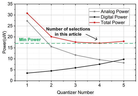
Figure 11.
Simulation of the relationship between the number of phase quantizers and chip power consumption.
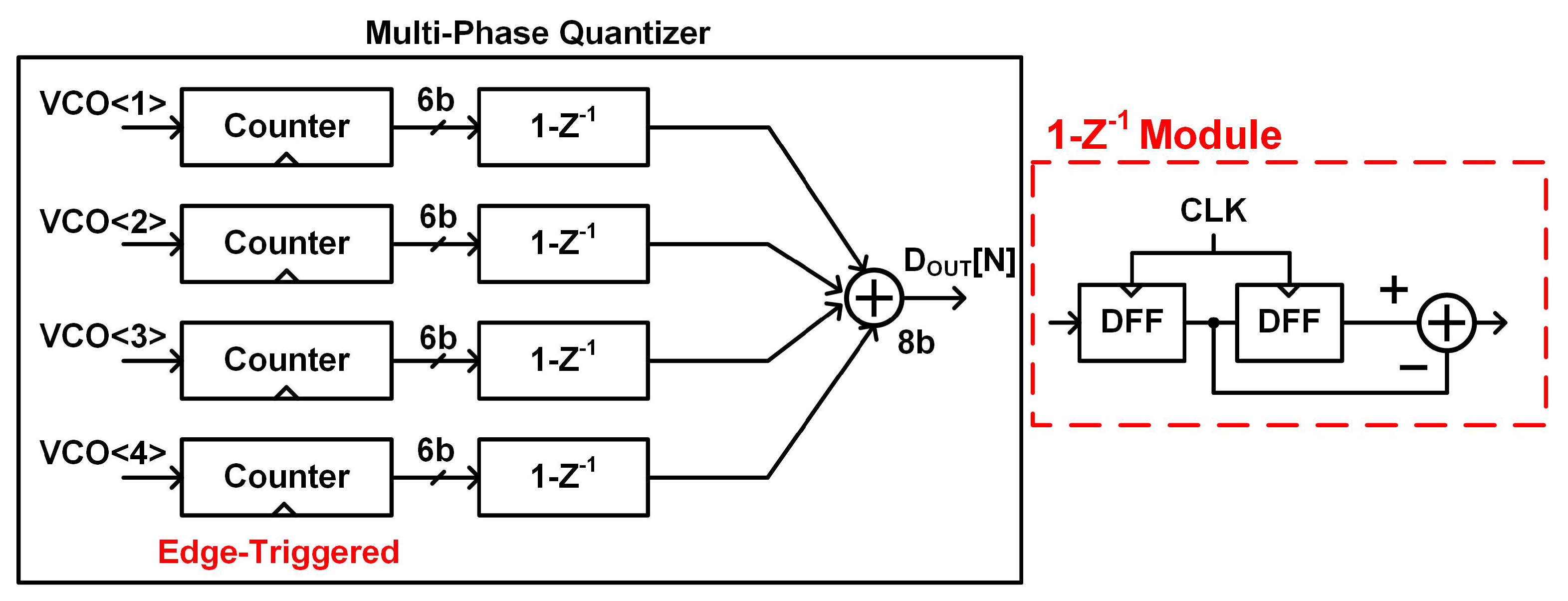
Figure 12 presents the schematic diagram of the VCO phase quantizer. The phase quantizer contains a counter that counts and samples the phases from the VCO simultaneously. After the end of a sampling period, the counter result is sent to a digital differencing circuit to implement first-order noise shaping. The digital differencing circuit consists of two sets of registers controlled by the same clock. The phase change of the VCO during a sampling period is obtained by subtracting the values of the two register sets. Finally, by summing the four sets of 6-bit values, an 8-bit output is produced.

Figure 12.
Schematic diagram of the VCO phase quantizer.
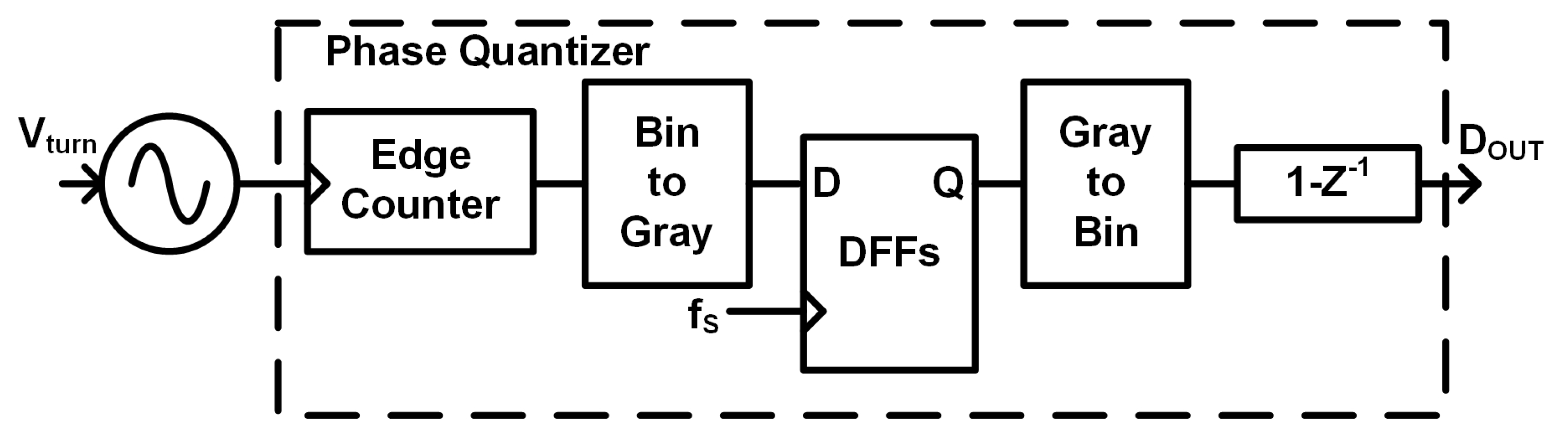
The DFF registers in the edge counter are triggered by the rising edges of . Due to non-idealities in the circuit, such as clock skew, the timing of the polarity transitions may slightly differ. The binary count output flips multiple bits in each transition. If the rising edge of coincides with the conversion in the edge counter, it may lead to large errors in the output of the DFF. To address this issue, the design incorporates Gray code encoding, as shown in Figure 13. After the edge counter, the binary count is first converted into Gray code, and, after passing through the DFF, it is converted back to binary. Since the Gray code only flips one bit at a time, even in the presence of metastability in the DFF, the errors can be constrained within one bit.
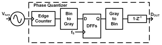
Figure 13.
Gray code coded phase quantizer.
2.5. Architecture of the Proposed Circuit
The simplified schematic of the proposed VCO-based ADC is shown in Figure 14. The input signal undergoes chopping and is then summed with the feedback signal. In order to improve the linearity, the amplitude of the summative residual signal is below 10 mV. The size of the residual signal VERR is usually determined by the loop coefficient, the DAC step size DAC, and the DAC jitter (1 LSB). It can be expressed as follows:
where N is the number of output bits of the ADC. It can be seen that the input signal , the reference voltage , and the output bit N together determine the size of the . The input range of the chip can be calculated as
where is the reference voltage of , is the capacitance of the total DAC, and is the AC coupling capacitance of the input end. Similarly, the IRN of the chip can be expressed as
where is the parasitic capacitance of the input difference pair, and is the IRN of the VCO quantizer. From Formulas (10) and (11), it can be observed that a larger ratio of to increases the chip’s input range, enhancing its ability to withstand the impact of EDO, but at the expense of degrading the chip’s input referred noise performance. Therefore, a trade-off must be made between the chip’s input range and IRN.
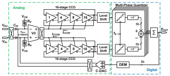
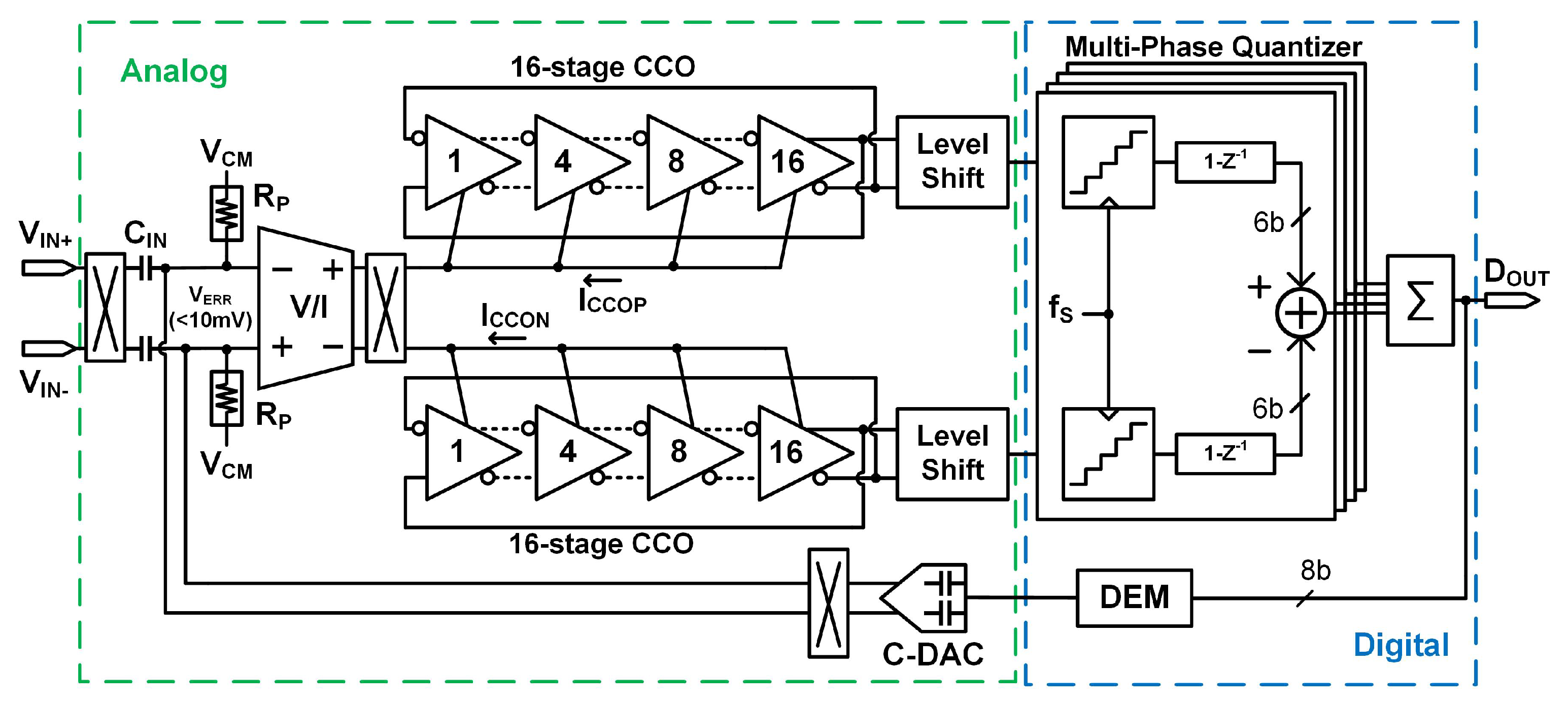
Figure 14.
Simplified schematic of the proposed VCO-based ADC.
The V/I conversion circuit converts the residual signal into the corresponding current signal to control the oscillation frequency of the CCO. The CCO consists of 16 cascaded differential delay cells, and the oscillating signal is converted into a digital signal by a level shifter circuit. Four phase quantizers sample and quantize the cascaded CCO at intervals of every 4 delay cells, with the sampling frequency set at 256 kHz. Subsequently, a digital differencing circuit is employed to achieve first-order noise shaping. The final digital output is obtained by summing the outputs of the four quantizers. A DEM structure is implemented in the feedback loop to mitigate capacitance mismatch. The entire circuit is primarily divided into digital and analog domains, with all digital logic being implemented in Verilog and synthesized using standard digital design methodologies.
3. Measurement Results
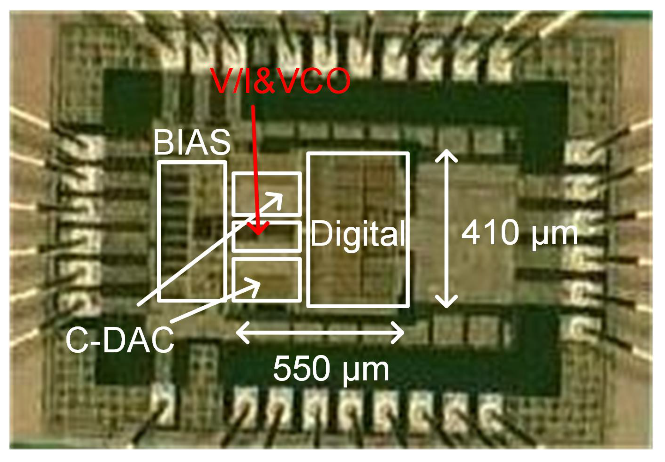
The circuit proposed in this paper is implemented using CMOS 180 nm technology with a core area of 0.225 mm2 (550 m × 410 m). Figure 15 is a microscopic view of the proposed circuit. As shown in Figure 15, the area of the analog part of the V/I and VCO circuit (250 m × 55 m) is only 1/8 that of the digital circuit (280 m × 410 m), indicating that the circuit proposed in this paper is highly digital. The entire chip achieves power consumption of 17.1 W under a power supply voltage of 1.8/1 V. Through simulation verification, if only one quantizer is used to quantize the VCO, the power consumption of the analog section exceeds 20 W. The proposed multi-quantizer structure reduces the analog power consumption to 9.6 W, while the digital circuit consumes 7.5 W. In more advanced processes, the power consumption and area of the digital circuit can be further reduced.
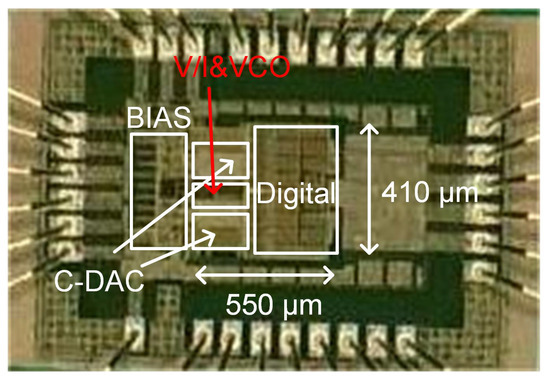
Figure 15.
Microscopic view of the proposed circuit.
Figure 16 presents the test PCB and testing environment for a first-order multi-quantizer ADC chip based on a VCO. On the PCB shown in Figure 16a, the chip’s inputs, power, and clock are all externally provided. An APx555 audio analyzer, serving as a pure signal source, is used to input an analog differential sine wave signal to the chip. As shown in Figure 16b, the output of the chip is a differential 8-bit output, which is connected to a logic analyzer, the 16802A (Agilent, Santa Clara, CA, USA). Finally, the output spectrum is calculated by MATLAB R2022b in a PC.
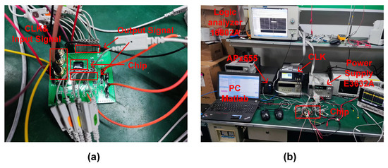
Figure 16.
First-order VCO test diagram: (a) test PCB, (b) test environment.
The performance parameters of the ADC were tested using an APx555 audio analyzer as an ultra-low distortion signal source, generating a 100 m amplitude and 1.375 kHz sine wave. In total, 524,288 points of the output signal were subjected to FFT, and the resulting output spectrum is shown in Figure 17. Within a 5 kHz bandwidth, the ADC achieved an SNDR of 62.1 dB and an SFDR of 65.1 dB. The presence of a digital first-order differentiator affected the ADC, resulting in a first-order noise shaping effect of 20 dB/decade.
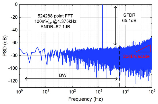
Figure 17.
Measured ADC output spectrum.
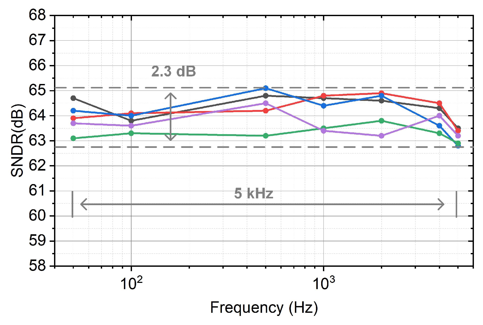
As shown in Figure 18, the relationship between the SNDR of the proposed ADC and the input frequency was measured across a bandwidth of 50 Hz to 5 kHz. As indicated by Formula (5), derived in the text, the precision of the ADC is influenced by the size of the VCO parasitic capacitance due to process variations. To lend more credibility to the test data, multiple samples were measured. The results demonstrate that within the 5 kHz frequency range, the variation in the SNDR across multiple samples remains within an acceptable margin of 2.3 dB.

Figure 18.
Measured SNDR versus input frequency (5 samples).
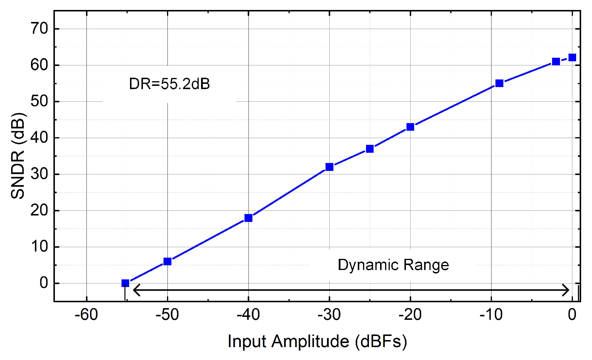
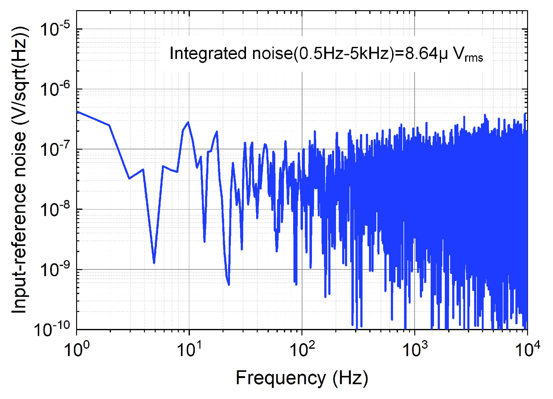
Figure 19 illustrates the measured SNDR versus the input amplitude, demonstrating the ADC’s dynamic range (DR) of 55.2 dB. Figure 20 presents the measured ADC input reference noise spectrum, which was measured at 8.64 within a 5 kHz bandwidth.

Figure 19.
Measured SNDR versus input amplitude.

Figure 20.
Measured ADC input-referred noise spectrum.
Table 1 presents a performance comparison with advanced technologies introduced in recent years. Compared to the IA+ADC architecture described in [27], this work achieves a lower area of 0.225 mm2 and power consumption of 17.1 W. In contrast to the ADC structure shown in [28], this paper realizes a higher input range and SNDR. While similar to [29] in terms of power consumption and SNDR, this work has managed to achieve an input range of 500 m by adjusting the feedback coefficients. The lower power consumption reported in [12,23] is based on the use of more advanced processes and narrower bandwidths, whereas our design supports a wider bandwidth of 5 kHz. The multi-channel structure discussed in [30] features very small per-channel areas, yet it falls short of our proposed architecture in aspects such as the input range and SNDR. Considering EDO and MAs, our study significantly exceeds the input range of approximately 100 m found in other studies by achieving a substantial 500 m. In summary, within the context of EEG signal recording circuits, the first-order VCO structure of the ADC introduced in our study is highly digitalized, offering superior adaptability to the demands of advanced technological nodes.

Table 1.
Comparison with the EEG signal recording circuit.
4. Conclusions
This paper presents a first-order noise shaping VCO-based ADC for the EEG signal recording front ends. To address the difficulty of applying analog integrators in advanced processes due to low voltages, a multi-phase quantizer structure is proposed to reduce the fc of the VCO to 1/2N, achieving lower analog power consumption with the same output bit resolution. The core area of the proposed circuit is 0.22 mm2, consuming 17.1 W, and it achieves a 62.1 dB SNDR and 10.02 bit ENOB within a bandwidth of 0.5–5 kHz, meeting the requirements of multi-channel EEG signal recording front ends. By introducing a form of Gray code encoding, the errors caused by circuit metastability are limited to within 1 bit. By employing digital differencing circuits, a first-order noise shaping effect is achieved, with input noise of 8.64 within the 0.5–5 kHz bandwidth. In view of the influence of MA and EDO, compared with the small input ranges of other EEG acquisition circuits, the circuit proposed in this paper achieves a large input range of 500 m, which greatly expands the application potential in the complex EEG recording environment. In summary, the EEG front end demonstrated in this paper holds significant research value and practical implications.
Author Contributions
Conceptualization, W.L. and Y.L.; methodology, W.L.; software, W.L., Y.H., X.W. and Y.L.; formal analysis, W.L.; writing—original draft preparation, W.L.; writing—review and editing, W.L. and Y.L.; supervision, Y.L. All authors have read and agreed to the published version of the manuscript.
Funding
This research received no external funding.
Data Availability Statement
The raw/processed data required to reproduce these findings cannot be shared at this time as the data also form part of an ongoing study.
Conflicts of Interest
The authors declare no conflicts of interest.
References
- Cheng, M.; Gao, X.; Gao, S.; Xu, D. Design and implementation of a brain-computer interface with high transfer rates. IEEE Trans. Biomed. Eng. 2002, 49, 1181–1186. [Google Scholar] [CrossRef] [PubMed]
- Lounasmaa, O.V.; Hamalainen, M.; Hari, R.; Salmelin, R. Information processing in the human brain: Magnetoencephalographic approach. Proc. Natl. Acad. Sci. USA 1996, 93, 8809–8815. [Google Scholar] [CrossRef] [PubMed]
- Yang, X.; Xu, J.; Chun, H.; Ballini, M.; Zhao, M.; Wu, X.; Van Hoof, C.; Van Helleputte, N. A 108 dB DR Hybrid-CTDT Direct-Digitalization ΔΣ-ΣM Front-End with 720mVpp Input Range and >300 mV Offset Removal for Wearable Bio-Signal Recording. In Proceedings of the 2019 Symposium on VLSI Circuits, Kyoto, Japan, 9–14 June 2019; pp. C296–C297. [Google Scholar]
- Chen, W.M.; Chiueh, H.; Chen, T.J.; Ho, C.L.; Jeng, C.; Ker, M.D.; Lin, C.-Y.; Huang, Y.-C.; Chou, C.-W.; Wu, C.Y.; et al. A Fully Integrated 8-Channel Closed-Loop Neural-Prosthetic CMOS SoC for Real-Time Epileptic Seizure Control. IEEE J. Solid State Circuits 2014, 49, 232–247. [Google Scholar] [CrossRef]
- Denison, T.; Consoer, K.; Santa, W.; Avestruz, A.-T.; Cooley, J.; Kelly, A. A 2 μW 100 nV/rtHz Chopper-Stabilized Instrumentation Amplifier for Chronic Measurement of Neural Field Potentials. IEEE J. Solid State Circuits 2007, 42, 2934–2945. [Google Scholar] [CrossRef]
- Muller, R.; Gambini, S.; Rabaey, J.M. A 0.013 mm2 5 μW DC-coupled neural signal acquisition IC with 0.5V supply. In Proceedings of the 2011 IEEE International Solid-State Circuits Conference, San Francisco, CA, USA, 20–24 February 2011; pp. 302–304. [Google Scholar]
- Muller, R.; Le, H.P.; Li, W.; Ledochowitsch, P.; Gambini, S.; Bjorninen, T.; Koralek, A.; Carmena, J.M.; Maharbiz, M.M.; Alon, E.; et al. 24.1 A miniaturized 64-channel 225 μW wireless electrocorticographic neural sensor. In Proceedings of the 2014 IEEE International Solid-State Circuits Conference Digest of Technical Papers (ISSCC), San Francisco, CA, USA, 9–13 February 2011; pp. 412–413. [Google Scholar]
- Gao, H.; Walker, R.M.; Nuyujukian, P.; Makinwa, K.A.; Shenoy, K.V.; Murmann, B.; Meng, T.H. HermesE: A 96-Channel Full Data Rate Direct Neural Interface in 0.13 μm CMOS. IEEE J. Solid State Circuits 2012, 47, 1043–1055. [Google Scholar] [CrossRef]
- Verma, N.; Shoeb, A.; Guttag, J.V.; Chandrakasan, A.P. A Micro-power EEG acquisition SoC with integrated seizure detection processor for continuous patient monitoring. In Proceedings of the 2009 Symposium on VLSI Circuits, Kyoto, Japan, 15–17 June 2009; pp. 62–63. [Google Scholar]
- Yazicioglu, R.F.; Merken, P.; Puers, R.; Van Hoof, C. A 200 μW Eight-Channel EEG Acquisition ASIC for Ambulatory EEG Systems. IEEE J. Solid State Circuits 2008, 43, 3025–3038. [Google Scholar] [CrossRef]
- Harrison, R.R.; Charles, C. A low-power low-noise CMOS amplifier for neural recording applications. IEEE J. Solid State Circuits 2003, 38, 958–965. [Google Scholar] [CrossRef]
- Huang, J.; Laiwalla, F.; Lee, J.; Cui, L.; Leung, V.; Nurmikko, A.; Mercier, P.P. A 0.01-mm2 Mostly Digital Capacitor-Less AFE for Distributed Autonomous Neural Sensor Nodes. IEEE Solid State Circuits Lett. 2018, 1, 162–165. [Google Scholar] [CrossRef]
- Lee, J.; Mok, E.; Huang, J.; Cui, L.; Lee, A.H.; Leung, V.; Mercier, P.; Shellhammer, S.; Larson, L.; Laiwalla, F.; et al. An Implantable Wireless Network of Distributed Microscale Sensors for Neural Applications. In Proceedings of the 2019 9th International IEEE/EMBS Conference on Neural Engineering (NER), San Francisco, CA, USA, 20–23 March 2019; pp. 871–874. [Google Scholar]
- Fan, Q.; Sebastiano, F.; Huijsing, J.H.; Makinwa, K.A.A. A 1.8 μW 60 nV/√ Hz Capacitively-Coupled Chopper Instrumentation Amplifier in 65 nm CMOS for Wireless Sensor Nodes. IEEE J. Solid State Circuits 2011, 47, 1534–1543. [Google Scholar] [CrossRef]
- Yazicioglu, R.F.; Merken, P.; Puers, R.; Van Hoof, C. A 60 μW 60nV/radicHz readout front-end for portable biopotential acquisition systems. In Proceedings of the 2006 IEEE International Solid State Circuits Conference, San Francisco, CA, USA, 6–9 February 2006; pp. 109–118. [Google Scholar]
- Verma, N.; Shoeb, A.; Bohorquez, J.; Dawson, J.; Guttag, J.; Chandrakasan, A.P. A Micro-Power EEG Acquisition SoC with Integrated Feature Extraction Processor for a Chronic Seizure Detection System. IEEE J. Solid State Circuits 2010, 45, 804–816. [Google Scholar] [CrossRef]
- Kassiri, H.; Salam, M.T.; Pazhouhandeh, M.R.; Soltani, N.; Velazquez, J.L.P.; Carlen, P.; Genov, R. Rail-to-Rail-Input Dual-Radio 64-Channel Closed-Loop Neurostimulator. IEEE J. Solid State Circuits 2017, 52, 2793–2810. [Google Scholar] [CrossRef]
- Chandrakumar, H.; Marković, D. A 15.2-ENOB 5-kHz BW 4.5-μW Chopped CT ΔΣ-ADC for Artifact-Tolerant Neural Recording Front Ends. IEEE J. Solid State Circuits 2018, 53, 3470–3483. [Google Scholar] [CrossRef]
- Bang, J.-S.; Jeon, H.; Je, M.; Cho, G.-H. 6.5 μW 92.3DB-DR Biopotential-Recording Front-End with 360 MVPP Linear Input Range. In Proceedings of the 2018 IEEE Symposium on VLSI Circuits, Honolulu, HI, USA, 18–22 June 2018; pp. 239–240. [Google Scholar]
- Kim, C.; Joshi, S.; Courellis, H.; Wang, J.; Miller, C.; Cauwenberghs, G. Sub-μ Vrms-Noise Sub-μW/Channel ADC-Direct Neural Recording with 200-mV/ms Transient Recovery Through Predictive Digital Autoranging. IEEE J. Solid State Circuits 2018, 53, 3101–3110. [Google Scholar] [CrossRef]
- Wu, R.; Chae, Y.; Huijsing, J.H.; Makinwa, K.A.A. A 20-b ± 40-mV Range Read-Out IC With 50-nV Offset and 0.04% Gain Error for Bridge Transducers. IEEE J. Solid State Circuits 2012, 47, 2152–2163. [Google Scholar] [CrossRef]
- Karkare, V.; Chandrakumar, H.; Rozgić, D.; Marković, D. Robust, reconfigurable, and power-efficient biosignal recording systems. In Proceedings of the 2014 IEEE Custom Integrated Circuits Conference, San Jose, CA, USA, 15–17 September 2014; pp. 1–8. [Google Scholar]
- Jiang, W.; Hokhikyan, V.; Chandrakumar, H.; Karkare, V.; Marković, D. A ±50-mV Linear-Input-Range VCO-Based Neural-Recording Front-End with Digital Nonlinearity Correction. IEEE J. Solid State Circuits 2017, 52, 173–184. [Google Scholar] [CrossRef]
- Lee, J.; Laiwalla, F.; Jeong, J.; Kilfoyle, C.; Larson, L.; Nurmikko, A.; Li, S.; Yu, S.; Leung, V.W. Wireless Power and Data Link for Ensembles of Sub-mm scale Implantable Sensors near 1GHz. In Proceedings of the 2018 IEEE Biomedical Circuits and Systems Conference (BioCAS), Cleveland, OH, USA, 17–19 October 2018; pp. 1–4. [Google Scholar]
- Leung, V.W.; Lee, J.; Li, S.; Yu, S.; Kilfovle, C.; Larson, L.; Nurmikko, A.; Laiwalla, F. A CMOS Distributed Sensor System for High-Density Wireless Neural Implants for Brain-Machine Interfaces. In Proceedings of the 2018—IEEE 44th European Solid State Circuits Conference (ESSCIRC), Dresden, Germany, 3–6 September 2018; pp. 230–233. [Google Scholar]
- Jayaraj, A.; Danesh, M.; Chandrasekaran, S.T.; Sanyal, A. Highly Digital Second-Order ΔΣ VCO ADC. IEEE Trans. Circuits Syst. I 2019, 66, 2415–2425. [Google Scholar] [CrossRef]
- Liu, X.; Zhang, M.; Richardson, A.G.; Lucas, T.H.; Van der Spiegel, J. Design of a Closed-Loop, Bidirectional Brain Machine Interface System With Energy Efficient Neural Feature Extraction and PID Control. IEEE Trans. Biomed. Circuits Syst. 2017, 11, 729–742. [Google Scholar] [CrossRef] [PubMed]
- Wendler, D.; De Dorigo, D.; Amayreh, M.; Bleitner, A.; Marx, M.; Willaredt, R.; Manoli, Y. A 0.0046-mm2 Two-Step Incremental Delta–Sigma Analog-to-Digital Converter Neuronal Recording Front End with 120-mVpp Offset Compensation. IEEE J. Solid State Circuits 2023, 58, 439–450. [Google Scholar] [CrossRef]
- Tu, C.-C.; Wang, Y.-K.; Lin, T.-H. A Low-Noise Area-Efficient Chopped VCO-Based CTDSM for Sensor Applications in 40-nm CMOS. IEEE J. Solid State Circuits 2017, 52, 2523–2532. [Google Scholar] [CrossRef]
- Wang, S.; Yang, X.; Wang, C.; Vilouras, A.; Lopez, C.M. A 0.00426 mm2 77.6-dB Dynamic Range VCO-Based CTDSM for Multi-Channel Neural Recording. Electronics 2022, 11, 3477. [Google Scholar] [CrossRef]


Disclaimer/Publisher’s Note: The statements, opinions and data contained in all publications are solely those of the individual author(s) and contributor(s) and not of MDPI and/or the editor(s). MDPI and/or the editor(s) disclaim responsibility for any injury to people or property resulting from any ideas, methods, instructions or products referred to in the content. |
© 2024 by the authors. Licensee MDPI, Basel, Switzerland. This article is an open access article distributed under the terms and conditions of the Creative Commons Attribution (CC BY) license (https://creativecommons.org/licenses/by/4.0/).