1. Introduction
Over the decades, progress in wide bandgap (WBG) devices, such as SiC and GaN, has facilitated further developments of electric vehicles, aircraft, and LIDAR systems. WBG devices can meet the challenging demands of these industries with high operating temperatures (over 250 °C), high current densities, rapid switching speeds, and high power requirements [
1,
2]. To ensure the performance and reliability of WBG devices, it is imperative that all packaging components adhere to more stringent thermal, electrical, mechanical, and reliability constraints [
3].
The die attachment process is crucial for ensuring the reliability of power modules utilizing WBG devices. Traditional die attachment materials, such as conductive adhesives and solder alloys, fail to meet the demands of WBG power devices due to their low melting temperatures and weak shear strength [
4]. Thus, it is necessary to explore alternative materials with higher melting points, improved thermal stability, and higher electrical conductivity, to ensure reliable connections in high-power-density applications.
Silver sintering is supposed to be a promising candidate, which offers lead-free interconnections with exceptional physical and chemical properties. Silver joints enable WBG devices to operate reliably at junction temperatures of 250 °C with high thermal and electrical conductivity [
5]. Silver also exhibits stable chemical properties and cannot be oxidized easily. The high melting temperature and reliability of silver joints endow it with significant advantages in high-power-density applications. Silver pastes used for silver sintering can be classified into two main categories according to the size of the silver particles, these being nanoscale silver paste and microscale silver paste. Nanoscale silver particles can be sintered at temperatures around 200 °C, with a maximum operating temperature of 600 °C. However, the high cost of nanoscale silver paste hinders its widespread application. To explore a cost-effective alternative, the development and application of micron-scale silver paste has become a current research topic.
Since the 1980s, when Schwarzbauer introduced silver sintering technology to power electronics, low-temperature silver sintering has gotten more and more attention as a die attachment process in WBG power modules [
6,
7,
8]. Traditional micron-scale silver sintering requires additional pressure and needs a longer processing time due to its lower surface energy, resulting in low efficiency. To obtain silver joints with high conductivity and reliability, a quasi-hydrostatic pressure of 30 MPa to 50 MPa is usually applied to the chip, which may lead to the fracturing of the substrate and the chip [
9].
To obtain high-quality micron-scale silver joints, researchers have explored various approaches. Zhang presents an alternative die attachment process for solder reflowing, which utilizes quasi-hydrostatically pressure-assisted sintering of silver pastes to lower the temperature [
10]. Bai demonstrated the high thermomechanical reliability of low-temperature sintered silver die attachment using a combination of die shear and thermal cycling experiments [
11]. Inoue used a bi-functional mercaptocarboxylate as the curing agent to induce low-temperature sintering of silver particles [
12]. Despite these methods, it is still challenging to obtain non-pressure-sintered micron-scale silver joints with high shear strength.
This paper presents a novel sintering process using IR to achieve rapid pressure-less sintering of micron-scale silver paste. IR has already been applied in electronics for the drying and curing of various materials [
13]. As shown in
Table 1, IR is categorized into short-wave, medium-wave, and long-wave according to its wavelength. The bandgap of GaN is 3.4 eV, and the corresponding photon wavelength is 365 nm resulting in high transmittance in the IR region. In actual situations, due to the existence of defects such as impurities, lattice defects, or interface defects, additional impurity energy levels will be introduced into the energy bands near the conduction and valence band, causing the absorption spectrum of photons to be broadened. Previous studies have shown that GaN and Si have high transmittance for visible light (wavelengths of approximately 400–700 nm). On the contrary, the transmittance of silver in the short-wave infrared light region (wavelengths of about 1–2.5 μm) is very low and mainly exhibits absorption characteristics [
14]. In order to ensure that IR can pass through the GaN power device and be absorbed by the silver paste and improve the quality of silver joints, this study selected short-wave IR with a wavelength of 1 um as the heating source. During the process of IR sintering, the temperature of the sinter paste increases faster than that of the chip and substrate. Due to the temperature difference, the evaporated solvent can easily volatilize through the gap between the chip and substrate to the outside, which further contributes to the lower porosity and higher shear strength of the IR-sintered joints [
15], achieving higher heating efficiency.
2. Materials and Methods
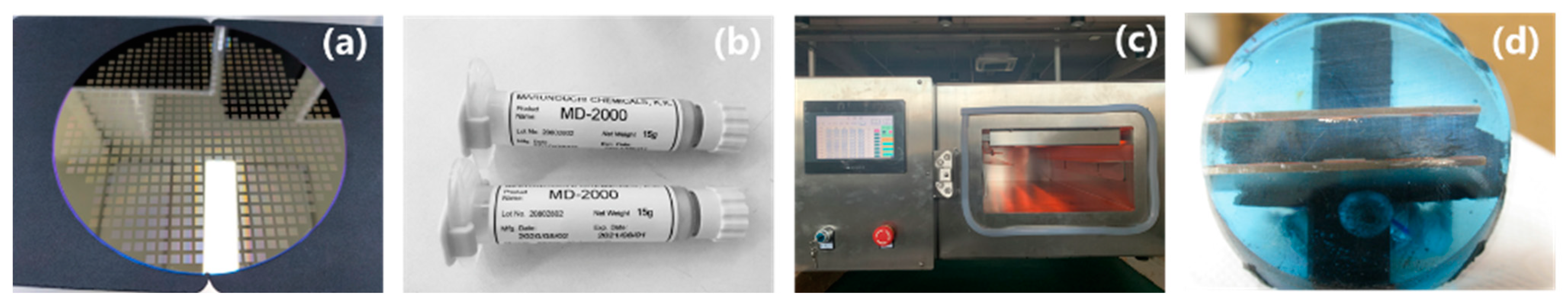
The samples used in this study are shown in
Figure 1. The silver metallized chips for die attachment had dimensions of 3.87 mm × 2.76 mm, which is shown in
Figure 1a.
Figure 1b presents the silver paste used in this study, whose silver particle sizes ranged from 1 μm to 3 μm. And this was applied to a direct copper bonding (DCB) substrate with a QFN lead frame.
Figure 1c shows the IR sintering oven used in this study. The wavelength of IR in silver sintering was set to 1 μm.
In the process of silver sintering, the main process parameters can affect the quality of the silver joints. Therefore, this study aims to investigate the influence of sintering process parameters on the IR-sintered silver joints and identify the optimal process parameters to optimize the sintering process.
Firstly, to investigate the influence of sintering temperature, the sintering temperature was set at 150 °C, 175 °C, 200 °C, 225 °C, 250 °C, 275 °C, and 300 °C, separately, while the sintering time was maintained at 45 min. To compare this with traditional sintering, the micro-silver paste was also sintered without pressure in a traditional oven at different sintering temperatures for 2 h. The heating rate during the entire sintering process was maintained at 26 °C/min.
Secondly, to explore the effect of sintering time, the silver paste was sintered in 5, 10, 15, 30, 45, and 60 min, separately, while the sintering temperature was maintained at 225 °C. The heating rate was kept at 26 °C/min.
In addition, in the sintering process, the heating rate also has an impact on the quality of the silver joints. Therefore, in this study, the sintering temperature was maintained at 225 °C, the sintering time was set to 45 min, and the heating rates were set at 20 °C/min, 23 °C/min, 26 °C/min, 29 °C/min, and 32 °C/min to investigate the effect of heating rate on the silver joints.
Furthermore, traditional silver sintering processes are typically conducted under a nitrogen atmosphere to prevent the formation of brittle metal oxides. In this study, the sintering temperature was maintained at 225 °C, the sintering time was set to 45 min, and the heating rate was fixed at 26 °C/min, the samples were sintered under both air and nitrogen atmospheres to compare the effect of the sintering atmosphere on the quality of the IR silver joints.
After determining the above sintering parameters, the micro-scale silver paste was sintered under different preheating conditions to further investigate the influence of pre-heating condition on the quality of the silver joints. The preheating temperatures were set at 70 °C, 90 °C, 110 °C, 130 °C, and 150 °C. Furthermore, the sintering temperature was set at 225 °C, the sintering time was 45 min, and the heating rate during the sintering process was maintained at 26 °C/min. Additionally, the micro-scale silver paste was also sintered under different preheating conditions in a traditional oven for 2 h as a comparison.
The shear strength of the joints was measured using a shear strength testing equipment (MFM1500, Deruiyin Precision Technology Company, Shenzhen, China) at a shear head speed of 50 μm/s. The shear height was fixed at 10 μm from the substrate surface. To calculate the porosity of the silver joints, the metallographic microscopy method was employed. Firstly, the silver joint samples were prepared and subjected to precision grinding and polishing to obtain smooth cross-sections, which is shown in
Figure 1d. Subsequently, the samples were observed using a metallographic microscope. The porosity can be calculated using the following formula: Porosity (%) = (Pore area/Total area) × 100. The cross-section samples of the joints were observed using a field emission SEM (FEI company NanoSEM650, FEI Company, Hillsboro, OR, USA).
3. Results
3.1. Mechanical Characteristics
High shear strength is crucial for ensuring reliable performance of sintered joints. Generally, the shear strength of silver joints is primarily influenced by the sintering process parameters, which include sintering temperature, sintering time, etc.
During the shear strength test, fracture often occurs at the weakest region between chip and substrate. According to the fracture region, fractures can be classified into five types: (1) a fracture inside the chip, (2) a fracture at the interface between the chip and silver joint, (3) a facture inside the silver joint, (4) a fracture at the interface between the substrate and silver joint, and (5) a fracture inside the substrate [
16]. The structure of the silver joint after the shear strength test was observed by upright metallurgical microscope (MX8R).
Figure 2 presents the image of the fracture surface of the IR-sintered silver joints after shear strength testing. Numerous island-like silver particles were observed on the DBC metal layer. The fracture of the IR-sintered joints occurred mostly at the interface between the metal layer and the sintered silver joint and a few fractures occurred within the sintered joints, which indicates a dense structure inside the silver joints.
During the IR sintering process, short-wave IR can penetrate through the GaN chip and heat the silver paste directly, leading to a dense structure. This dense structure can effectively improve the strength of the silver joint, thereby reducing the possibility of fractures inside the sintered joint and improving the reliability of the silver joint.
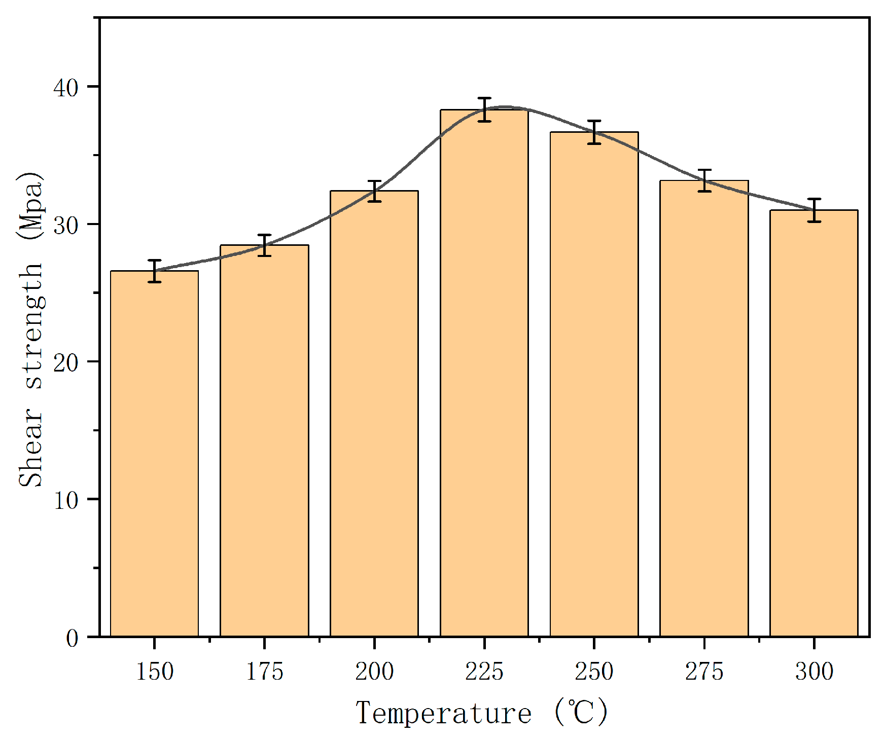
3.1.1. Sintering Temperature
Figure 3 shows the shear strength of IR-sintered silver joints of different sintering temperatures with a sintering time of 45 min. The results indicate that, as the sintering temperature increases, the shear strength of the IR-sintered silver joints initially rises until reaching its peak at a temperature of 225 °C, after which it starts to decline. While the traditional silver joints need to be sintered at 300 °C for 2 h to obtain silver joints with an equivalent shear strength of 38.29 MPa.
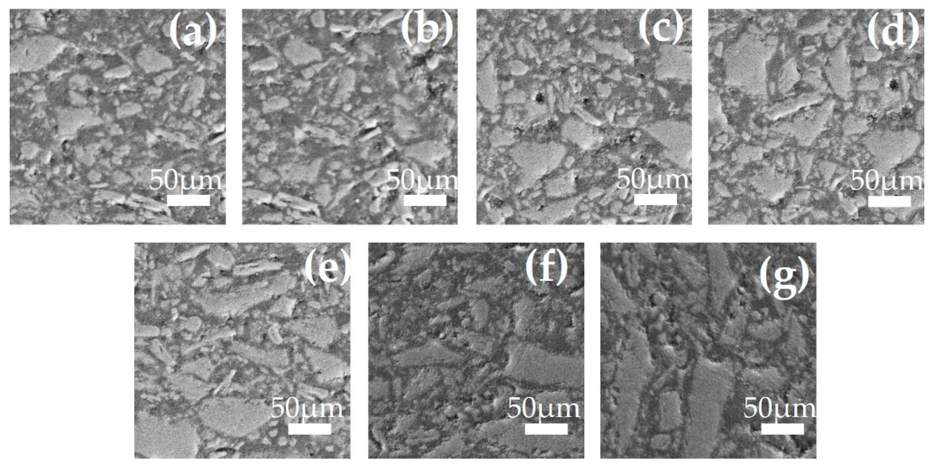
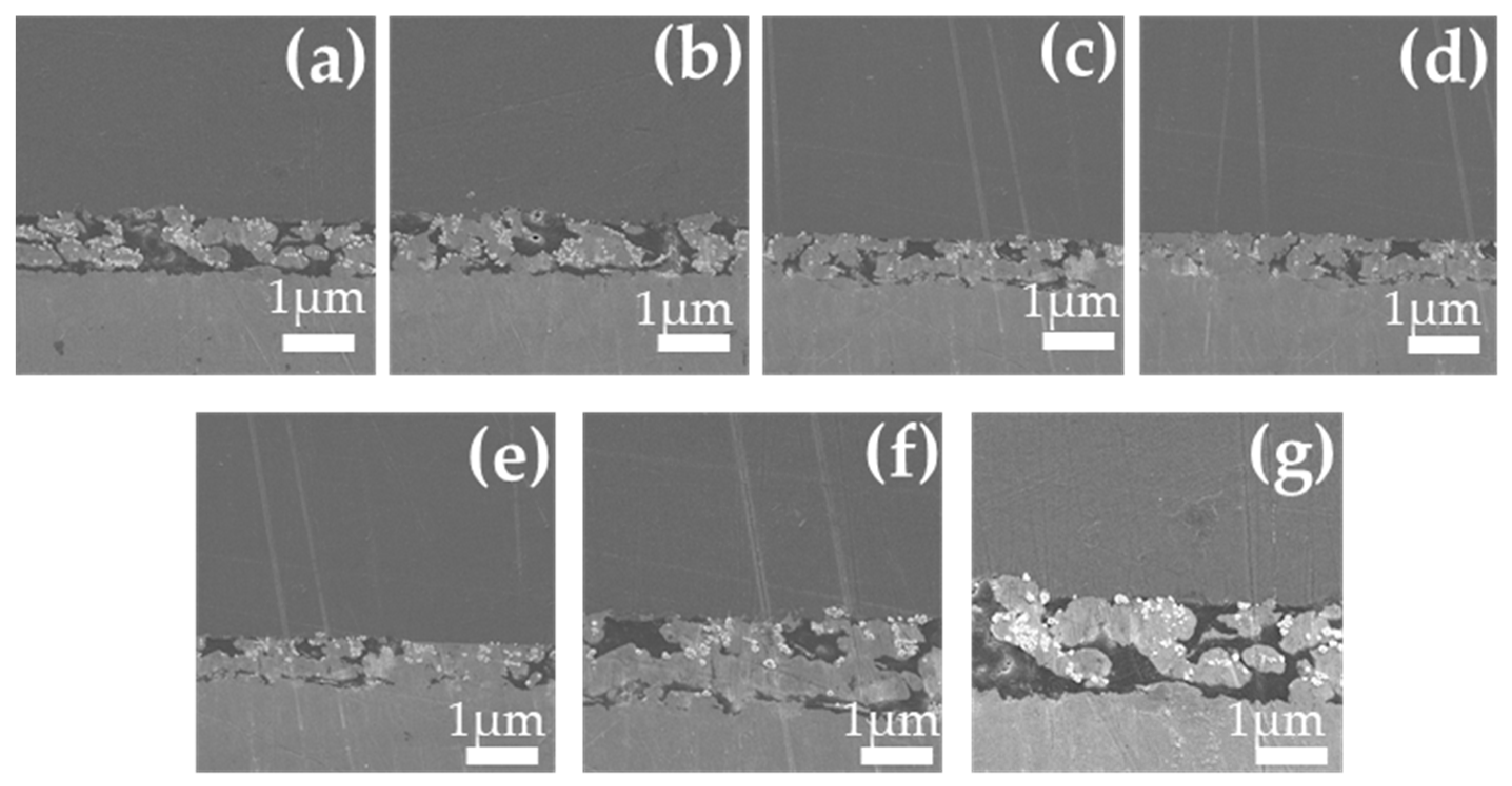
The shear strength of silver joints is primarily affected by their porosity. At a temperature of 150 °C, the porosity of IR-sintered silver joints was 22.47%, and this rapidly decreased to 5.1% at a sintering temperature of 300 °C. The structure of IR-sintered silver joints sintered at different temperatures is shown in
Figure 4, which shows that the silver joints became increasingly dense as the temperature increased. The reduction in porosity is quite valuable as it hinders the permeation of air and prevents the oxidation of the substrate metal, thereby enhancing the long-term stability and reliability of the joints. To test the reliability of the silver joints, they went through a thermal shock test. After 3000 cycles of thermal shocking, the porosity of the IR-sintered silver joints sintered at 225 °C did not change, remaining at 6.4%, showing a high reliability.
Similar to traditional sintering of micro-silver paste, increasing the IR sintering temperature can enhance the densification of microscale silver particles [
17,
18].
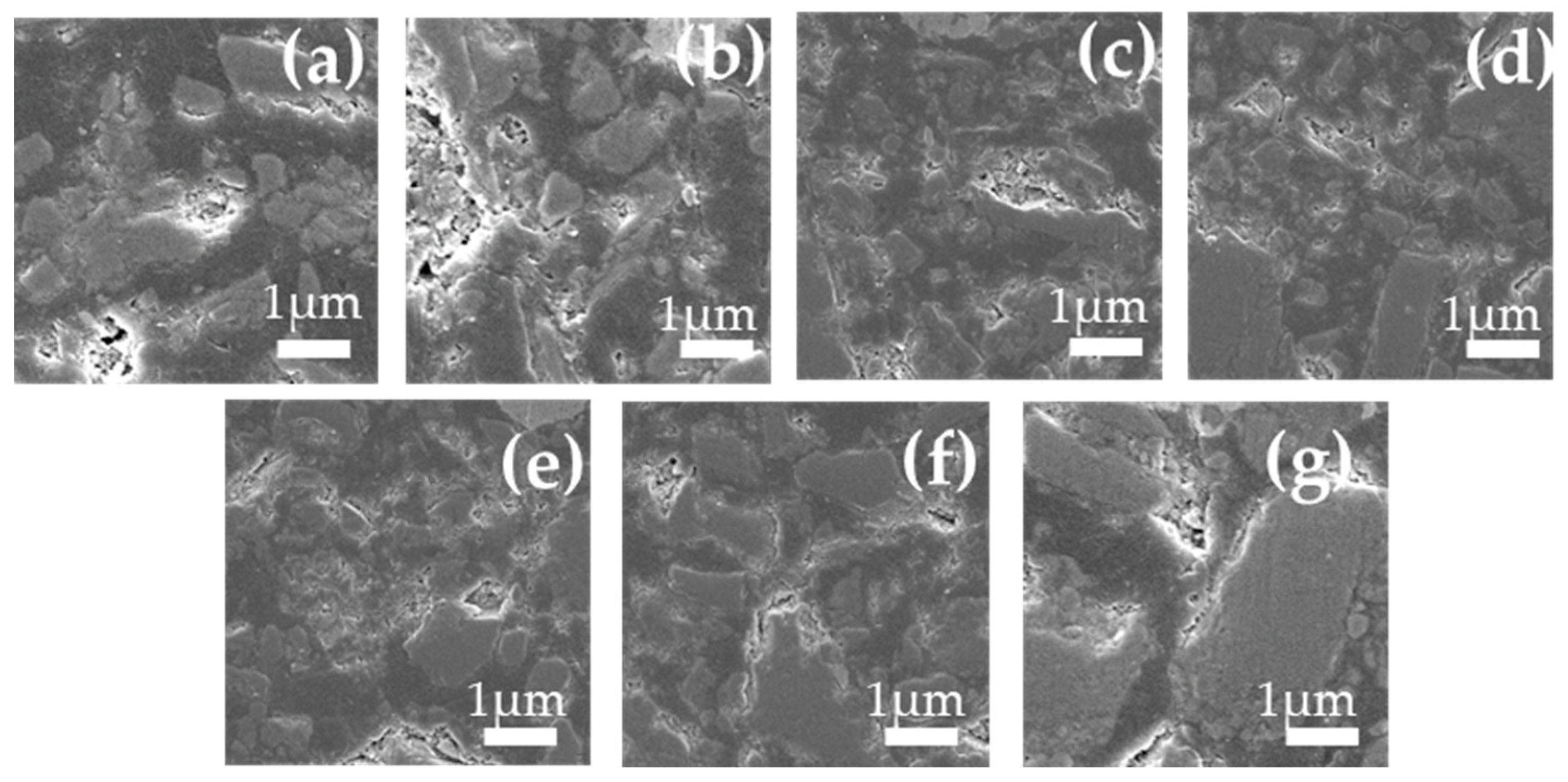
Figure 5 presents the microstructure of IR-sintered silver joints at different sintering temperatures. It can be seen that the samples sintered at 150 °C show an incomplete network structure which indicates inferior sintering quality compared to the other samples. With the temperature increasing, the joints undergo re-sintering, resulting in tightly connected silver particles, a coarse sintering network, and a decrease in impurities between the silver particles, which can be attributed to the reduction in organic films on the surface of the silver particles [
19]. Moreover, the necks within the network of silver joints thicken. The enlargement of neck diameter enhances the connection between particles, leading to improved shear strength. This observation of the microstructure proves that when the sintering temperature increases, the sintered network becomes more compact, which means as the sintering temperature increases, the shear strength of the joints should gradually increase.
However, as shown in
Figure 3, the maximum shear strength was observed at a temperature of 225 °C and then the shear strength decreased as the temperature kept increasing, which is not in line with the above theoretical inference. This is because the weakest part appeared at the interface between substrate and chip.
Figure 6 presents the microstructure of the interface between the silver joint and the substrate under different temperatures. The difference in the diffusion coefficient of silver and substrate metal resulted in Kirkendall voids, and increasing the temperature worsens this situation [
20]. As a result, the increase in voids at the interface between the substrate and the silver paste weakens the shear strength of the silver joints after 225 °C despite the internal structure of the silver paste becoming denser when the sintering temperature rises.
3.1.2. Sintering Time
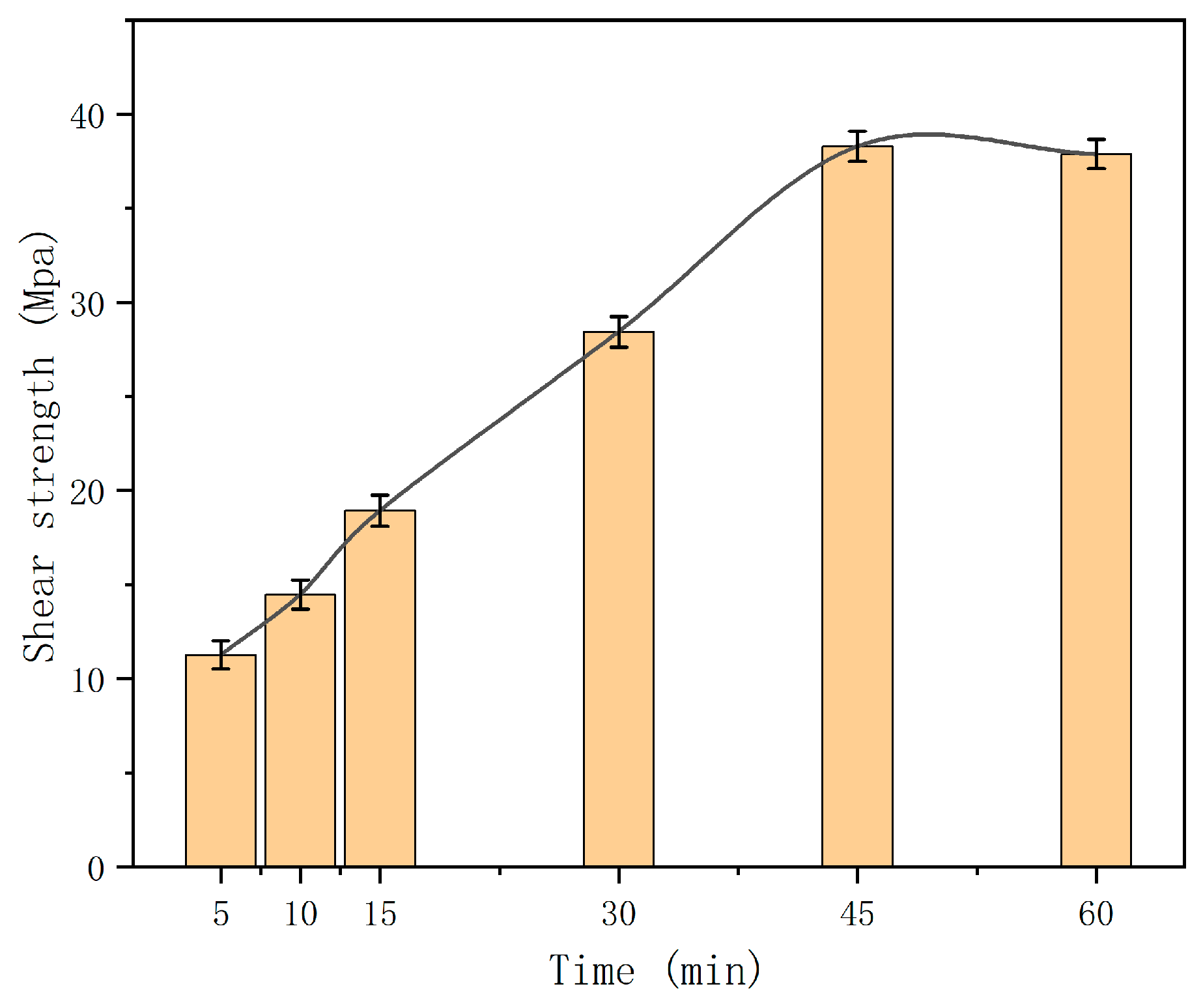
To explore the effect of sintering time, the silver paste was sintered for 5, 10, 15, 30, 45, and 60 min separately and the sintering temperature was set at 225 °C. The results are presented in
Figure 7. As the sintering time increases, the shear strength of the silver joints exhibits a rapid rise at first, and then remains stable from 45 min to 60 min. This indicates that adequate sintering time is necessary to enhance the strength of the silver joints, which is because the connections between the silver particles need enough time to form.
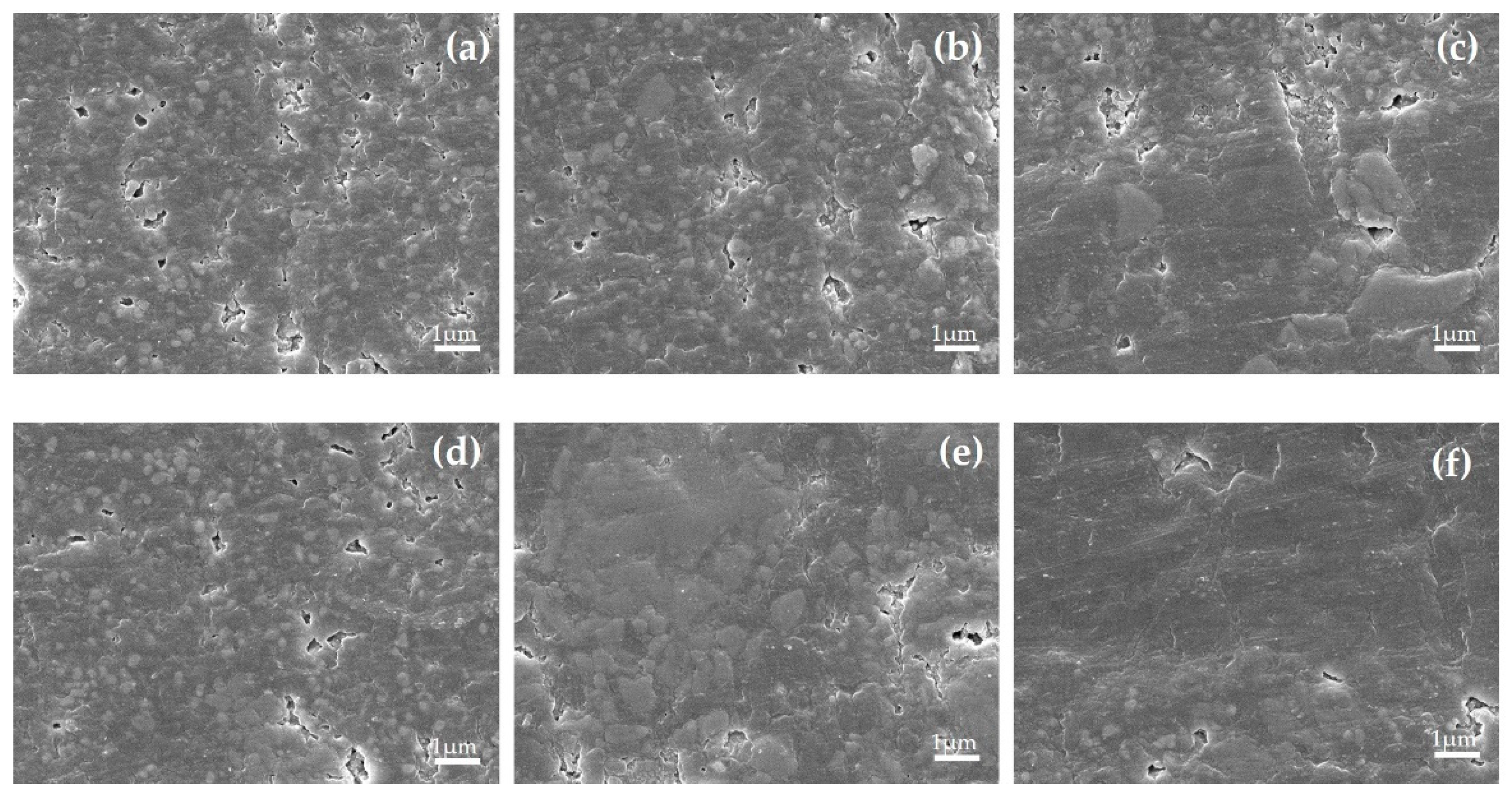
The internal structures of the IR-sintered silver joints were observed using SEM, and the results are shown in
Figure 8. With the sintering time increasing, the connection of silver particles becomes more compact which means that sufficient sintering time is necessary to enhance the strength of the silver joint. During the sintering process, the silver particles require adequate time to establish connections and densify. As the sintering time increases, the bonding between silver particles becomes stronger, thereby improving the shear strength. However, when the sintering time exceeds a certain threshold, the improvement in shear strength becomes less significant because the sintering process has completed [
21]. Therefore, to ensure the shear strength of the silver joint, the sintering time for IR sintering should not be less than 45 min.
3.1.3. Heating Rates
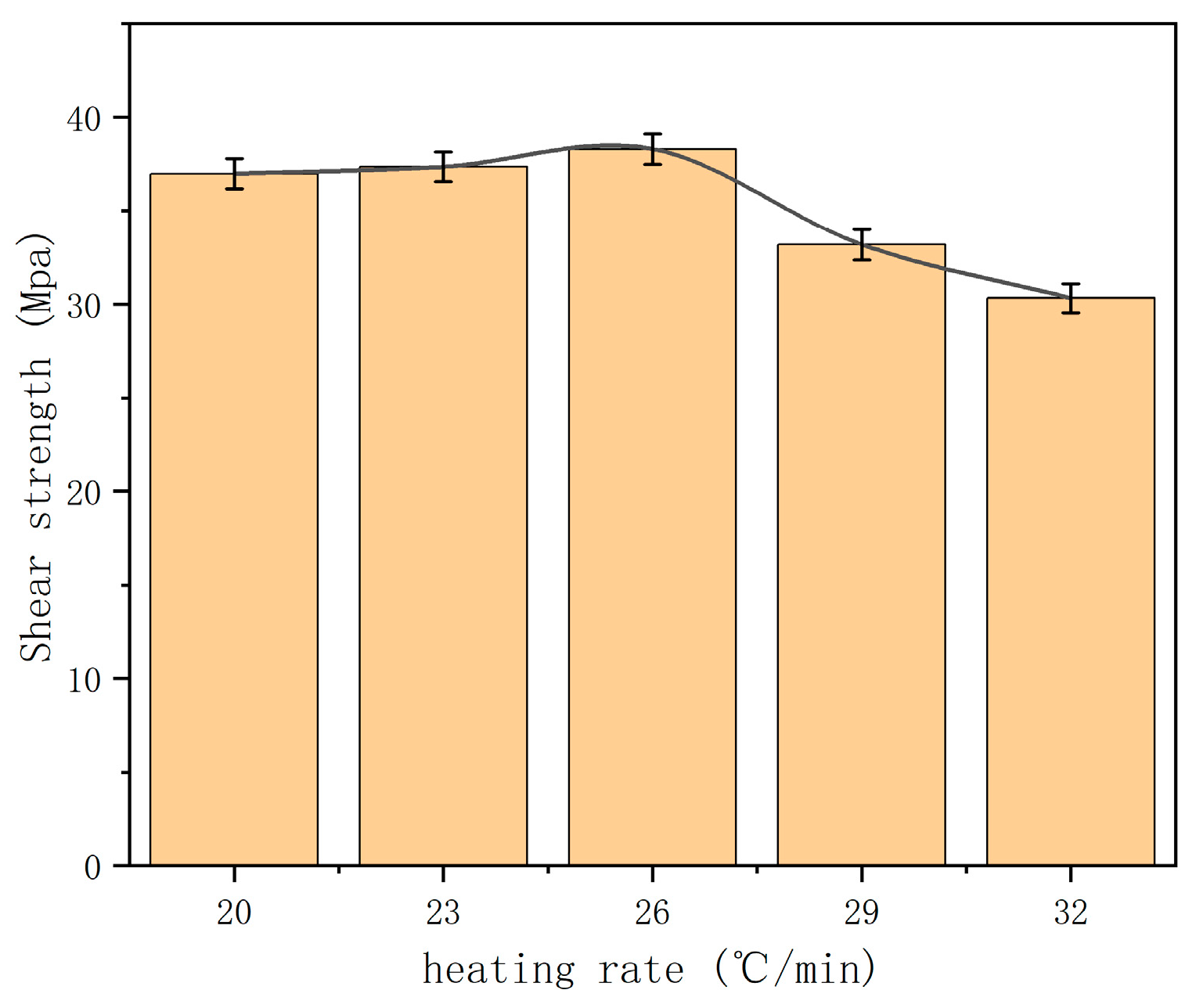
The shear strength of IR-sintered silver joints sintered at different heating rates is shown in
Figure 9. It can be observed that the shear strength of the IR silver joints initially increases and then decreases as the heating rate rises; the maximum shear strength was observed at the heating rate of 26 °C/min. The silver particles can have enough time to be sintered at an appropriate heating rate, which promotes the formation of a larger and more uniform structure. This contributes to improving the strength of the silver joint. However, an excessively slow heating rate can lead to the oxidation of the silver particles, thereby decreasing the densification of the silver joint during sintering.
Additionally, an excessively high heating rate will result in uneven nucleation and growth of silver particles, increasing the internal stress and thermal stress within the silver joint, leading to a decrease in the shear strength of the silver joint [
22]. A heating rate of 26 °C/min is observed to be the best heating rate in this study, as it ensures the densification of the silver joint and prevents the oxidation of the silver particles, resulting in the highest shear strength.
3.1.4. Sintering Atmosphere
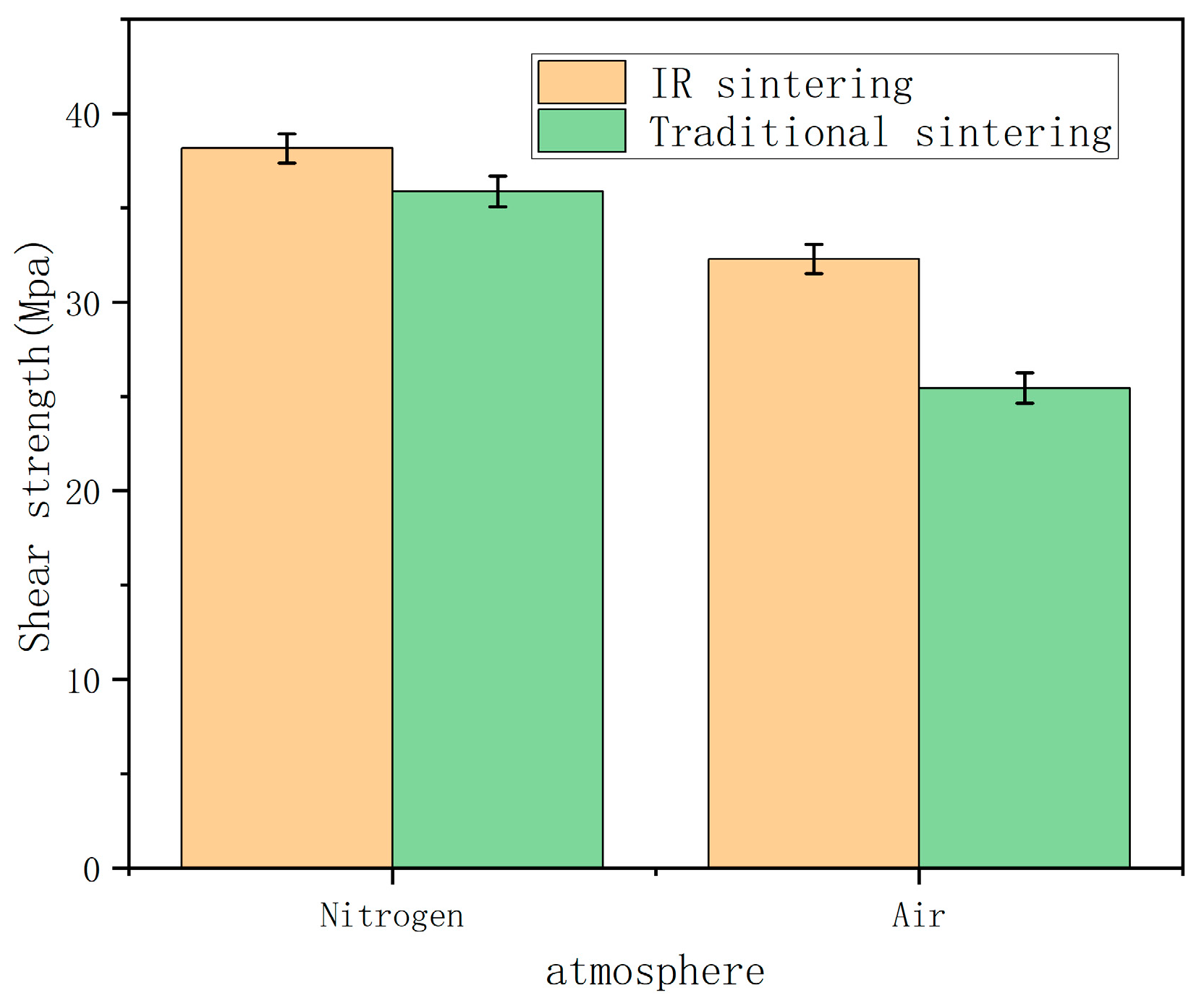
Figure 10 illustrates the shear strength of IR-sintered silver joints sintered under different atmospheres. It can be observed that in both IR sintering and traditional sintering, the shear strength of silver joints sintered in a nitrogen atmosphere is higher than those sintered in an air atmosphere. This indicates that the protection provided by an inert gas atmosphere can prevent oxidation during the sintering process, thereby enhancing the quality of the silver joint.
Furthermore, the shear strength of the silver joints obtained through IR sintering in nitrogen is 18.14% higher compared to those sintered in an air atmosphere, while in traditional sintering, the difference amounts to 41%. This is because IR sintering can heat silver paste directly, which raises the temperature of the silver paste higher than the temperature of the surrounding environment, promoting the evaporation of the internal gas. This helps protect the silver particles from oxidation. Thus, the shear strength of the IR-sintered silver joint is less sensitive to the sintering atmosphere.
3.1.5. Preheating Temperatures
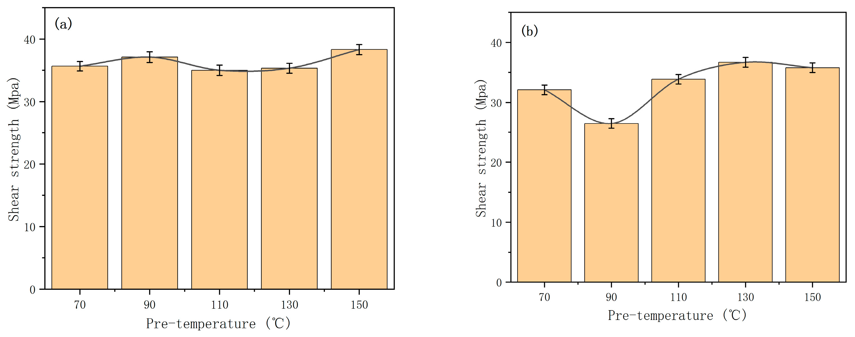
The shear strength of silver joints sintered at different preheating temperatures is presented in
Figure 11. It can be observed that the shear strength of the silver joints obtained through IR sintering remains around 38 MPa as the preheating temperature increases. However, in the process of traditional sintering, the shear strength of silver joints is influenced by the preheating temperature. As the preheating temperature increases, the shear strength of traditional sintered silver joints initially decreases and then increases, reaching a maximum shear strength of 36.68 MPa at a sintering temperature of 130 °C, which is slightly lower than the average shear strength of IR-sintered joints.
The above observation result is due to the different heating models of traditional sintering and IR sintering. The traditional silver sintering process indirectly heats the silver paste by heating the surrounding atmosphere, making it difficult for the internally generated gases to escape as the surrounding air temperature is higher than the silver paste. Therefore, in the traditional sintering process, the silver paste needs to be preheated before sintering to allow the internal gases to volatilize in advance. In contrast, short-wave IR can transmit through GaN chip to heat the silver paste directly, which enables the silver paste to heat up faster than the chip and substrate, accelerating the volatilization of internal organic solvents and moisture and decreasing the internal porosity of silver joints [
15]. Thus, the shear strength of IR-sintered silver joints is less sensitive to preheating temperatures. Consequently, in the IR sintering process, the preheating process can be appropriately shortened, which reduces the overall processing time and enhances production efficiency.
3.2. Electrical Characteristics
The resistivity of sintered silver joints is another critical parameter to evaluate its performance in die attachment. A low resistivity means there are more conductive paths, which indicates a better formation of sintered joints [
23].
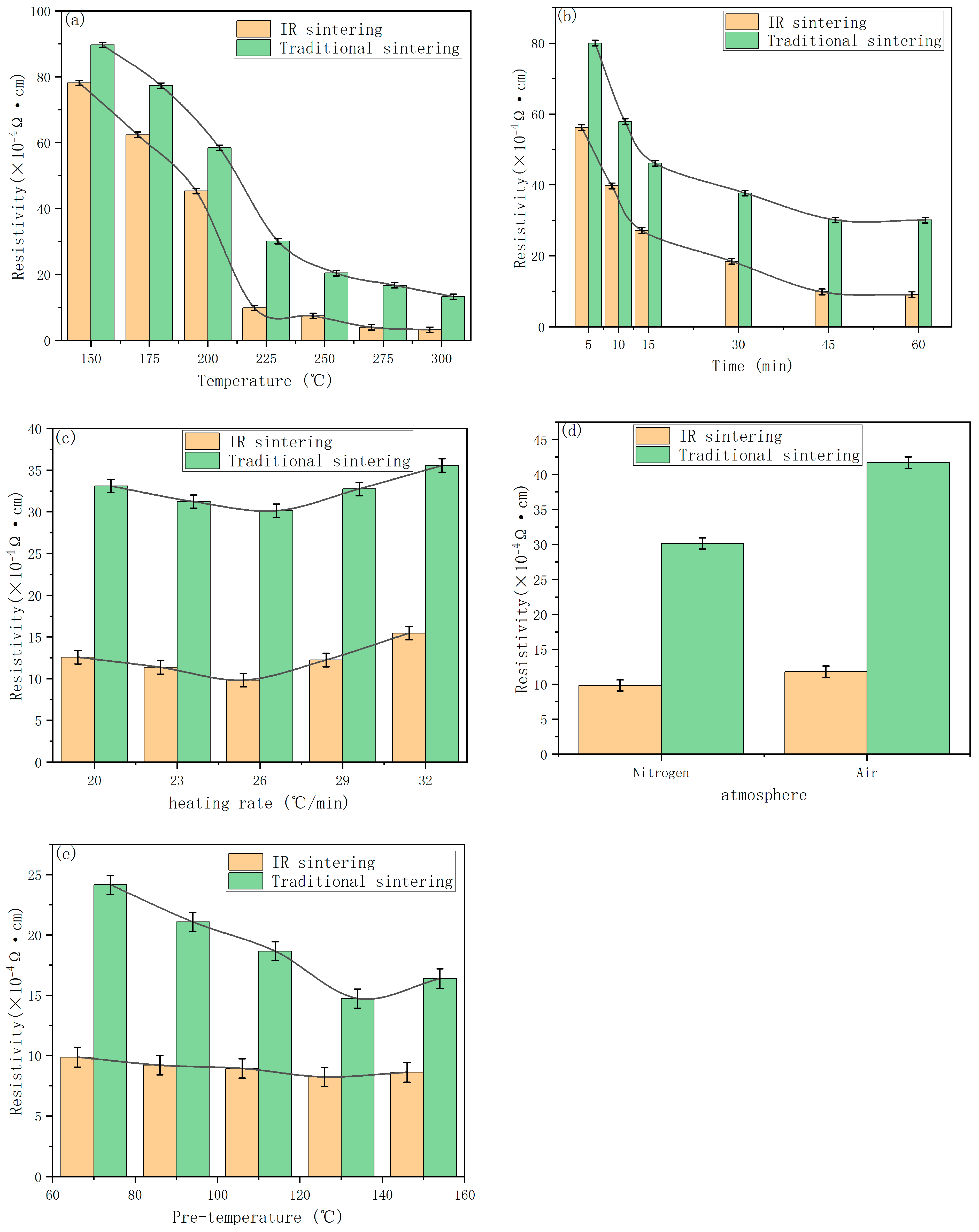
The resistivity of silver joints at different sintering temperatures is shown in
Figure 12a. The resistivity of silver joints decreases as the sintering temperature increases. This is because increasing sintering temperature contributes to enhancing the bonding between the silver particles and the substrate metal, reducing contact resistance, thereby lowering the overall resistivity. Moreover, as sintering temperature increase, the diffusion of silver particles is enhanced, forming a denser structure, which further reduces the resistivity [
24]. For comparison, the resistivity of traditional sintered silver joints is also recorded in
Figure 12a. It can be seen that the IR-sintered silver joints exhibit lower resistivity compared to traditional sintered silver joints at the same sintering temperature.
It is worth noting that the resistivity of silver joints abruptly decreased from 7.82 × 10⁻⁴ Ω·cm (150 °C) to 9.83 × 10⁻⁵ Ω·cm (225 °C) at first, then slightly decreased to 7.41 × 10⁻⁵ Ω·cm, 3.97 × 10⁻⁵ Ω·cm, and 3.22 × 10⁻⁵ Ω·cm at temperatures of 250 °C, 275 °C, and 300 °C, respectively.
To investigate the reason why the resistivity decreasing rate changed, the silver joints obtained at different temperatures were observed by SEM (
Figure 5a–g). During the sintering process, the silver particles interconnect each other, forming considerable conductive pathways to transmit electrons. When the sintering temperature was below 225 °C, the number of conductive pathways inside the silver joints increased rapidly as the sintering temperature rose. However, when the sintering temperature increased continuously, the number of pathways in the silver joints remained relatively constant and the conductive pathways started to thicken. The number of pathways has a greater impact on the resistivity than the thickness [
25].
Figure 12b shows the resistivity of IR-sintered silver joints after different sintering times. With the sintering time increasing, the resistivity of the IR-sintered silver joints decreased at first and then stabilized. To obtain silver joints with a low resistivity, the sintering should not last less than 45 min.
Figure 12c presents the resistivity of IR-sintered silver joints under different heating rates. As the heating rate increases, the resistivity of the silver joints initially rises and then decreases, reaching a peak at a heating rate of 26 °C/min. This phenomenon is consistent with the trend of the shear strength of the silver joints with heating rate.
The resistivity of silver joints sintered under different atmospheres is shown in
Figure 12d. It can be observed that the resistivity of IR and traditional silver joints sintered in a nitrogen atmosphere is lower than that of those sintered in an air atmosphere. Moreover, the resistivity of silver joints obtained by IR sintering in the nitrogen atmosphere is 20.23% lower than those sintered in the air atmosphere, while the traditional silver joints exhibit a difference of 38.44%, indicating that the sintering atmosphere has less impact on the resistivity of IR-sintered joints.
Figure 12e illustrates the influence of preheating temperature on the resistivity of silver joints obtained through IR sintering and traditional sintering, respectively. It can be observed that, as the preheating temperature increases, the resistivity of the silver joints gradually decreases. It is worth noting that the resistivity of IR-sintered silver joints remains relatively stable at different preheating temperatures. In contrast, the lowest resistivity for the traditionally sintered silver joints is attained at 130 °C with a fluctuation of 46.15%. These results indicate that, compared to the traditional sintering process, IR sintering is less sensitive to preheating temperature due to its ability to promote the volatilization of organic solvents within the silver paste [
26].
3.3. Performance of Power Device
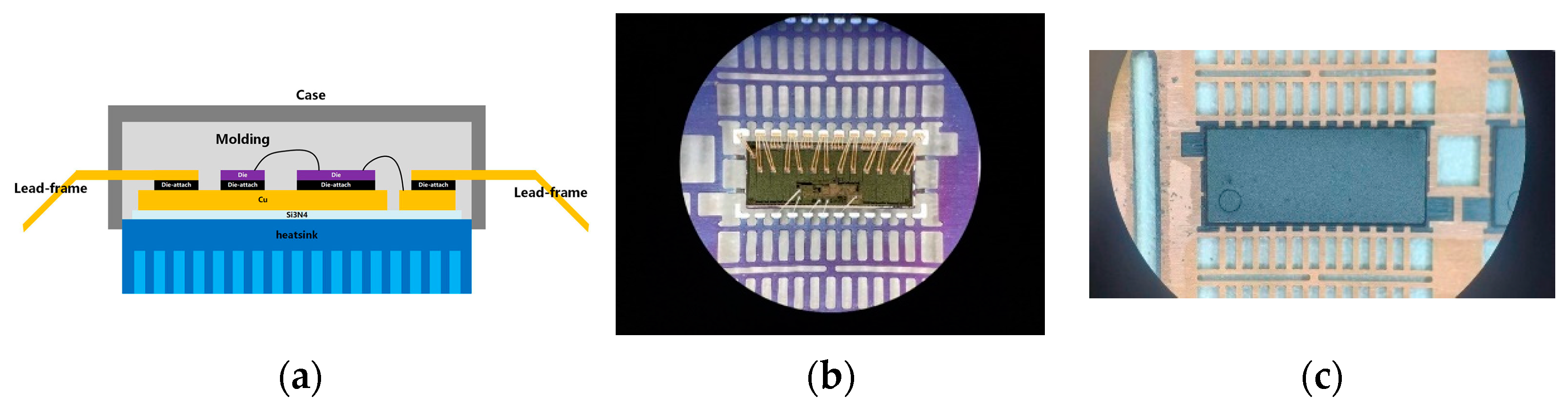
To investigate the influence of IR sintering on the performance of power devices, the GaN die was bonded to the substrate using an IR sintering process, followed by system-in-package (SOP) encapsulation.
Figure 13 illustrates the cross-sectional schematic of the SOP package, while
Figure 13b,c show the internal and external physical top views of the SOP package. The packaging components of the GaN power device include the GaN die, the SOP lead frame, the micron-scale silver solder joints, gold wires, etc.
3.3.1. Thermal Resistance
The conduction resistance of a GaN power device is significantly influenced by its operating temperature. Excessive operating temperatures can cause performance degradation or the malfunction of the device. Therefore, the thermal dissipation capability and temperature distribution of power devices were investigated in this paper.
The power supply voltage of the GaN power device was set to 13.5 V and the load resistance was set to 2.1 Ω. An infrared thermal analyzer was used to detect the operating temperature of the GaN power device. The infrared thermal image of the power device is shown in
Figure 14a. It can be observed that when the power device reaches a stable operating condition, the highest temperature appeared at the center of the operational region, gradually decreasing towards the edges of the power device. The maximum operating temperature was 59 °C.
When a voltage is applied to the gate of the GaN power device, two-dimensional electron gas (2DEG) forms inside the GaN power device, resulting in current flow. Under the influence of the thermal effect, thermal electrons are generated within the GaN device. As the temperature rises, the motion of hot electrons intensifies, leading to collisions with the lattice, resulting in the generation of phonons. Phonons, in turn, undergo scattering, generating more hot electrons, achieving the transfer of thermal energy [
27]. During the operation of the GaN power device, the highest electric field occurs at the gate region. Thus, the collisions between electrons, phonons, and the lattice occur most frequently in the gate region, forming the primary heat source. In practical applications, it is crucial to focus on the heat generation in this region [
28].
The infrared thermal image of a traditionally sintered GaN power device is shown in
Figure 14b. Compared to GaN power devices obtained through IR sintering, the traditionally sintered GaN power device exhibits more hotspots, and its highest operating temperature rises 14 °C, which indicates that the IR-sintered silver joints have lower resistance, enhancing the thermal performance of the GaN power device.
3.3.2. Electrical Performance
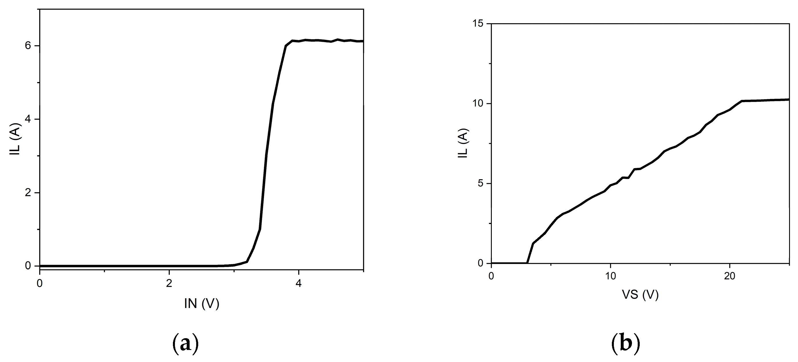
The DC performance of a GaN power device was tested firstly when the power supply voltage was set to 13.5 V, and the load resistance was set to 2.1 Ω.
Figure 15 shows the DC characteristics curve of the GaN power device. It can be seen that the threshold voltage for the input signal to switch the device into the on-state is 2.9 V. Under normal operation, the gate-source voltage of the GaN power transistor is 4.3 V and the output current is 6.415 A. It is worth noting that the on-state conduction resistance of the GaN power device is only 4 mΩ, indicating that the GaN power device exhibits a low resistance when it is on, enabling more efficient power transfer and lower power consumption. This low on-state resistance is one of the advantages of GaN power devices, providing improved switching performance and power efficiency.
Furthermore, during the testing process, as the power supply voltage gradually increases, the voltage drop of the GaN power device also increases. From calculations, it can be determined that, under such a circumstance, the on-state resistance of the GaN power device increases continuously, as depicted in
Figure 16. This indicates that, during the testing process, the on-state resistance of the GaN power device increases with rising temperature due to thermal effects, leading to performance degradation.
A GaN power device obtained through a traditional silver sintering process was also tested. Under the same operating conditions, the GaN power device obtained through the IR sintering process exhibited lower on-state resistance compared to the power device obtained through the traditional sintering process. This indicates that the IR sintering process improves the quality of the silver joint, thereby improving the performance of the GaN power device under high-power conditions.
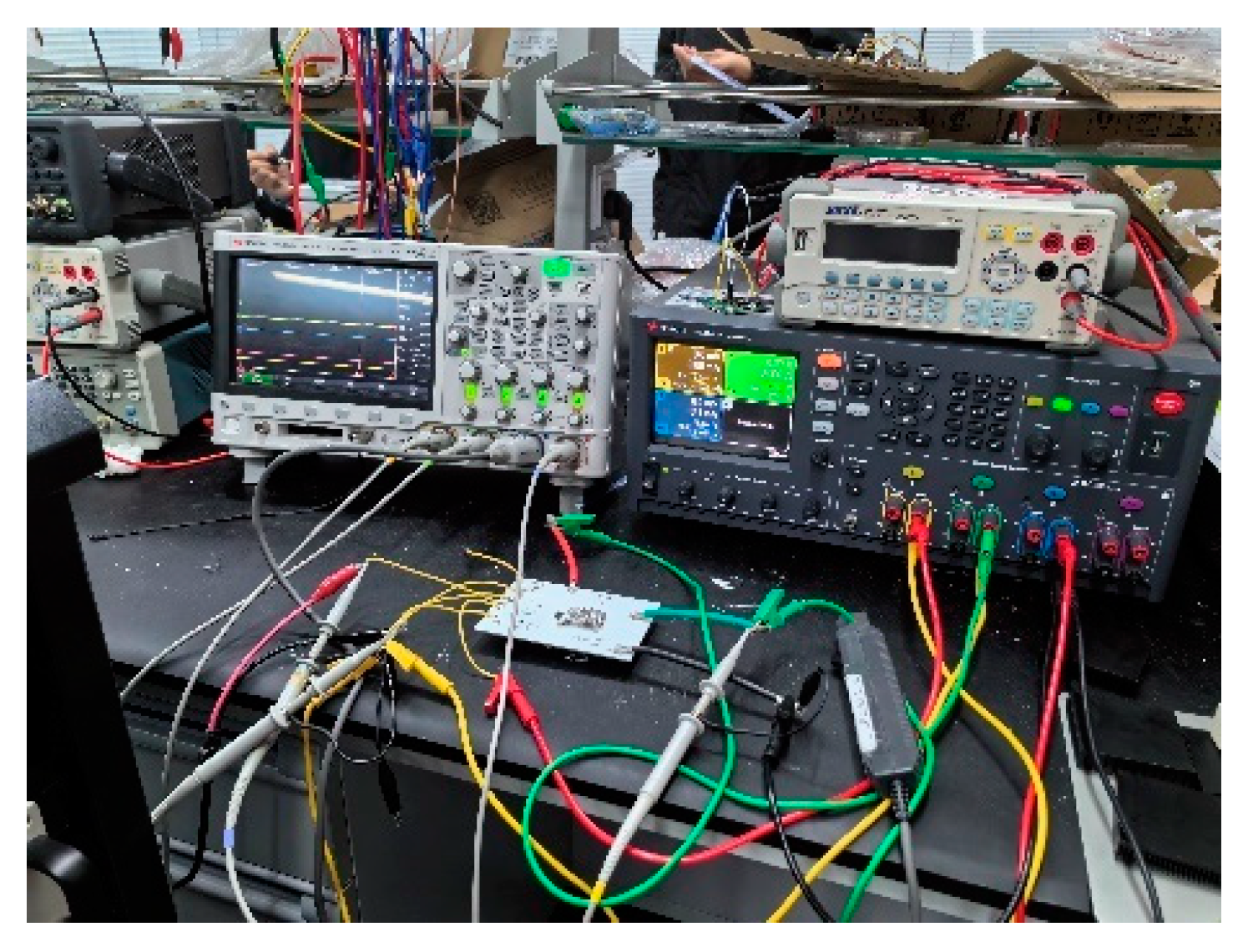
The dynamic performance of GaN power devices was also tested in this paper. The equipment used in the testing is shown in
Figure 17, including the function generator, DC power supply, and digital filter.
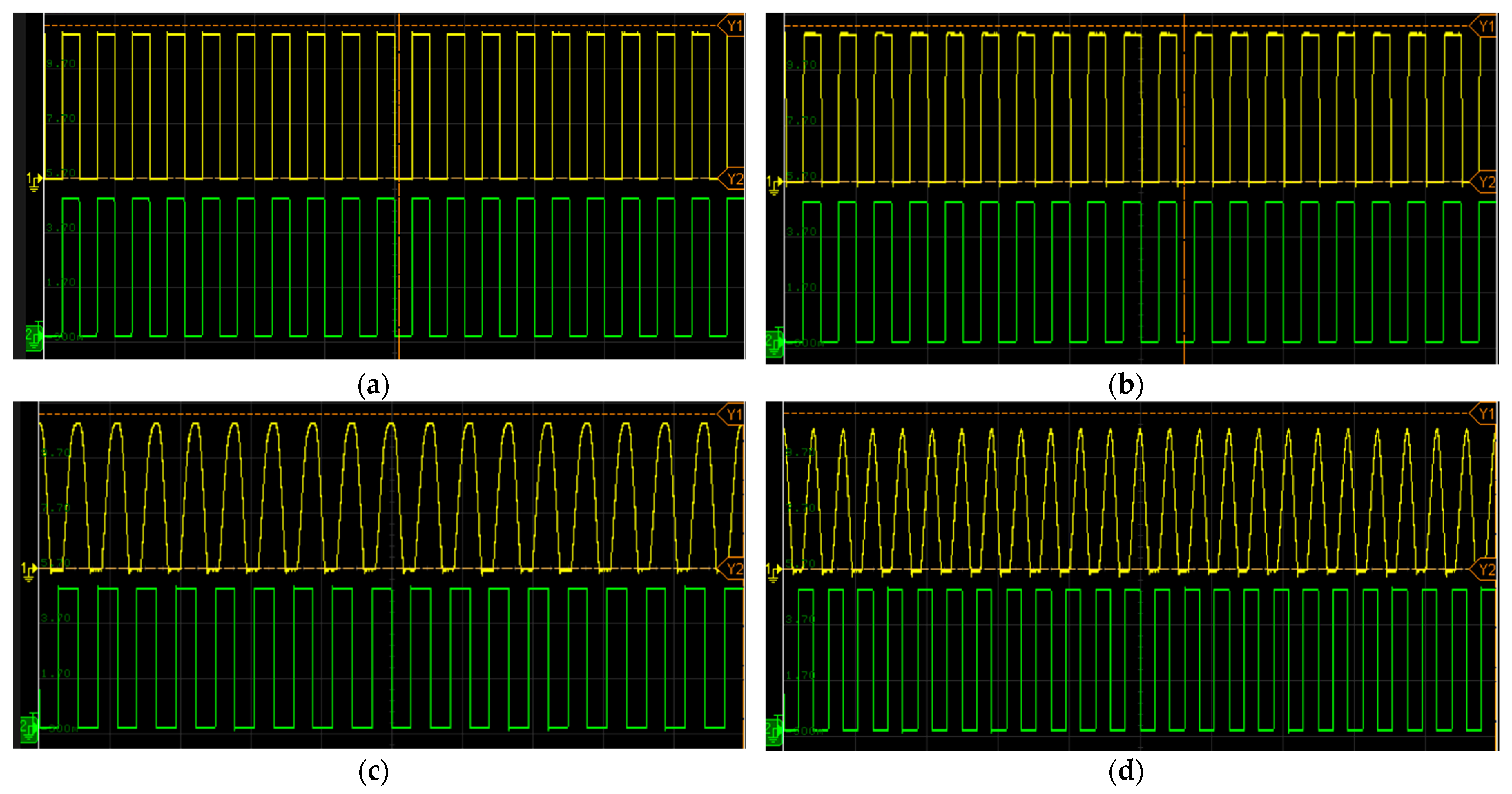
The frequency range of the input signal was set from 1 MHz to 10 MHz. The test results are presented in
Figure 18, where
Figure 18a–d correspond to the test results at input frequencies of 1 MHz, 3 MHz, 5 MHz, and 10 MHz, respectively. In
Figure 18, Channel 1 displays the output signal waveform of the GaN power device, while Channel 2 shows the input signal waveform.
When the input signal frequency is below 3 MHz, the output signal of the GaN power device is relatively ideal without distortion. However, the distortion becomes apparent as frequency increases. This can be attributed to factors such as parasitic capacitance and inductance within the device.
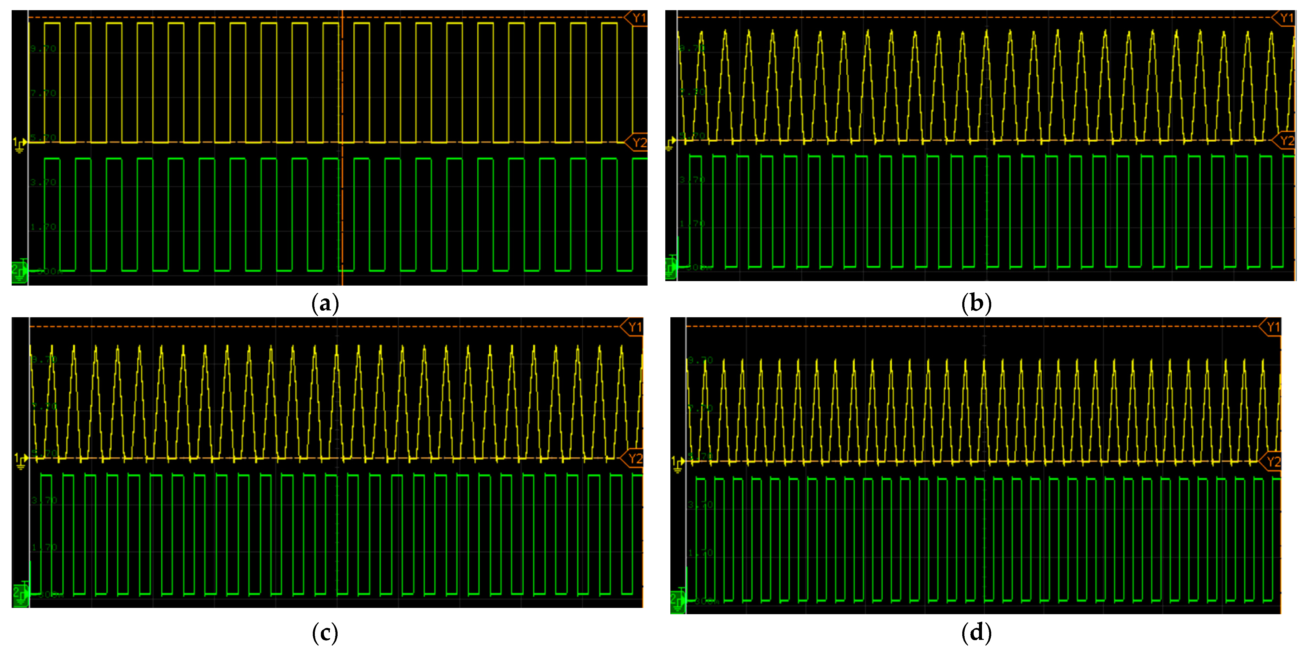
Figure 19 presents the test results of GaN power devices obtained through a traditional sintering process. Compared to GaN power devices obtained through IR sintering, the traditional GaN power device exhibits sever distortion when the input signal is at 3 MHz. This indicates that IR sintering technology can provide better high-frequency characteristics and improve the dynamic response of the device. This is because the structure of the IR-sintered silver joint is more compact, facilitating signal transmission and heat dissipation. The denser silver joint structure can provide lower parasitic resistance and inductance, reducing power loss and interference during signal transmission, which helps maintain signal accuracy and integrity, reducing the occurrence of distortion. Additionally, high-frequency operation generates significant power dissipation and increases the temperature of the device. However, the IR-sintered silver joint structure offers better thermal conduction paths, thus reducing the operating temperature of the device. This thermal improvement enhances the reliability and stability of the device, reducing the possibility of distortion during high-frequency operation [
29]. Therefore, the GaN power device obtained through IR sintering exhibits better high-frequency characteristics.
4. Discussion
During the process of IR sintering, IR energy can transmit through the chip and heat the silver paste directly, which accelerates the volatilization of organic solvents and moisture within the silver paste, resulting in a decrease in the porosity of the silver joints. In comparison to that, traditional sintering indirectly heats the silver paste by heating the surrounding environment. Thus, the silver joints need to be preheated before sintering so that the organic solvents and moisture have enough time to escape, increasing the processing time. As a result, to obtain silver joints with a shear strength of 38.29 MPa, the total processing time for IR sintering is approximately 45 min, which is significantly shorter than the 2 h traditional sintering process.
Silver sintering is a process in which silver particles are consolidated to form dense joints at temperatures far below the melting temperature of silver [
30,
31]. For the sintering kinetics, it relies on thermodynamic potential from the high surface free energy of the silver particles and atomic transport [
32]. In the process of silver sintering, cohesion and adhesion are identified as the predominant factors. In summary, cohesion is the result that the reduction in surface Gibbs free energy of silver particles drives the process of particle consolidation and densification sintering [
30].
In general, there are two kinds of adhesive mechanisms, adhesion theories and particle adhesion theories, including chemical bonding, diffusion, solid solubility, mechanical interlocking, physical adsorption, the van der Waals force, the electrostatic force, the capillary force, and magnetic attractions, etc. [
33]. Usually, adhesion mechanisms can be narrowed down to chemical bonding, interdiffusion, solid solubility, and mechanical interlocking because the other forces have a minimal impact on silver sintering.
Chemical bonding can be categorized into metallic bonds, ionic bonds, covalent bonds, coordinate bonds, hydrogen bonds, etc. [
33]. In the process of silver sintering, only the metallic bonds need to be considered. To obtain a high shear strength, silver particles must formulate solid metallic bonds over a large contact area. In the process of sintering, with the temperature rising, the surface energy of silver particles increases and the atomic motion intensifies, leading to the formation of metallic bonds at the interface. After the initial formation of bonds in the contacted region, the contact area expands laterally on the solid surface driven by the densification of silver particles [
34].
Diffusion is the gradual mixing of material from a higher concentration region to a lower concentration region caused by random molecule mobility [
33]. The motivation of interfacial adhesion is to lower the interfacial and surface Gibbs free energy, which requires atomic diffusion across the interface and on the surface. The rate of atomic diffusion, quantified by the diffusivity (
D), is highly influenced by temperature according to the Arrhenius expression.
where
Q is the activation energy, and
D0 is a term determined by atomic vibration frequency and jump distance.
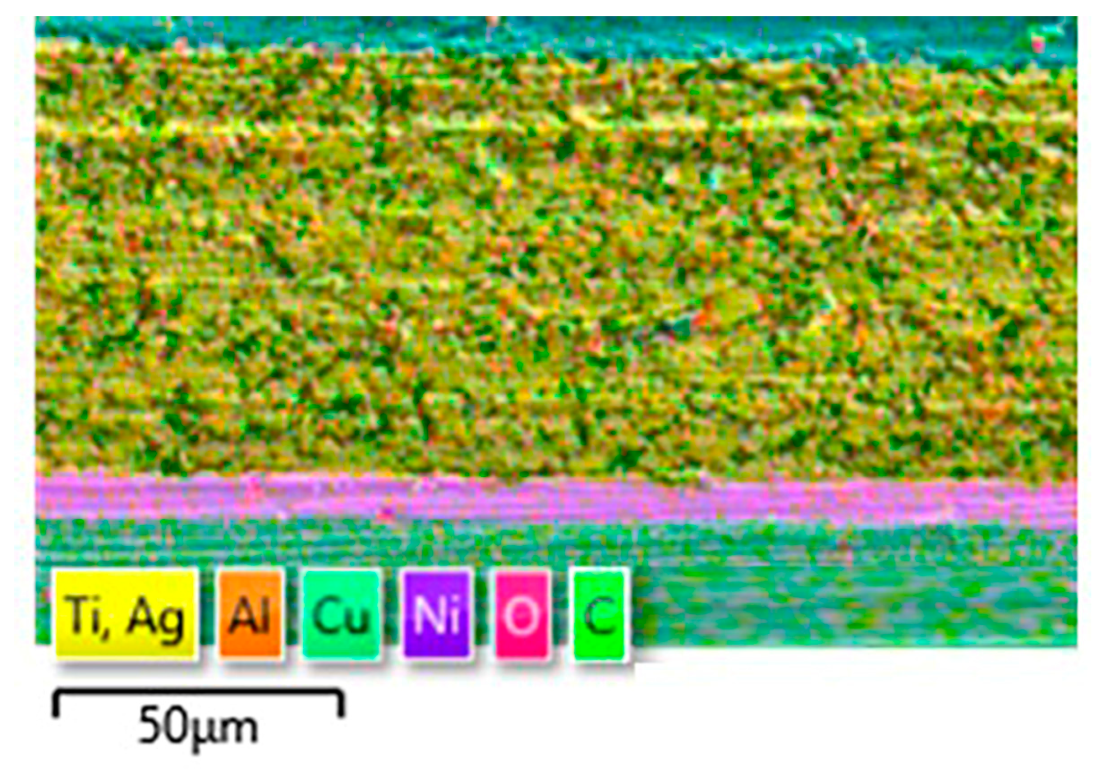
Figure 20 shows the EDS result for an IR-sintered silver joint. It can be observed that the substrate metal contacting the silver connector is mainly Ni.
Table 2 lists the inter-diffusivities for several common metals, which are based on the literature [
35,
36]. As listed in
Table 2, the diffusivity of Ag into Ni is much lower than that of Ni into Ag. As a result, there would be Kirkendall voids at the contact area. At first, the connections between the silver paste and substrate become denser because the formation of the silver joint occupies a dominant position. When the temperature is higher than 225 °C, the voids at the interface begin to increase, reducing the contact area of the silver joint. Furthermore, the Kendall effect may cause metal diffusion and reaction to form intermetallic compounds, leading to embrittlement and crack formation in the silver joint, reducing the shear strength and electrical conductivity of the silver joint. Thus, the temperature of IR sintering should not be higher than 225 °C. Additionally, this study also conducted IR sintering of GaN dies at different temperatures and tested their thermal and electrical performance. The results revealed that, under the same operating conditions, GaN power device sintered at 225 °C exhibited the lowest operating temperature, the lowest on-resistance, and the most stable high-frequency characteristics. Thus, to obtain reliable silver joints, the IR sintering temperature should be set at 225 °C. However, the optimal sintering temperature for the traditional micron-scale silver sintering process without pressure typically falls around 300 °C. This is because, the silver particles have absorption characteristics that match well with short-wave IR, which can be efficiently absorbed by silver particles and converted into heat energy, enabling sintering at a lower temperature. In contrast, traditional sintering methods may require higher temperatures to ensure sufficient heat transfer to the silver particles. Traditional heat sources, such as furnaces or electric ovens, often result in uniform heating of the entire environment, leading to unnecessary energy loss. Therefore, the optimal sintering temperature for IR silver sintering is lower than that of traditional sintering processes.
5. Conclusions
This study investigates the feasibility of utilizing IR for silver sintering and provides an alternative method to non-pressure sintering processes for micro-scale silver paste. The results show that the shear strength of IR-sintered joints sintered for 45 min achieves 38 MPa, which is higher than the traditional joints obtained by about 2 h of non-pressure sintering in a convection oven. Therefore, IR sintering can reduce the process time significantly and enhance the quality of the silver joints.
To optimize the IR sintering process, the influence of sintering parameters including temperature, time, heating rate, atmosphere, and preheating temperature on the quality of silver joints was investigated. It can be determined that, to obtain reliable silver joints, the micro-scale silver paste should be sintered in a nitrogen atmosphere at a sintering temperature of 225 °C for at least 45 min where the heating rate is set at 26 °C/min.
It was worth noting that, as the sintering temperature increases, the shear strength of the silver joints initially increases and reaches a peak at 225 °C. And further temperature increase leads to a decline in shear strength due to the enhanced interdiffusion between substrate metal and silver particles, which results in an increase in voids. What is more, the decline rate in the resistivity of silver joints also decreases with increasing sintering temperature. This is because, at lower temperatures, a raising temperature can increase the number of conductive pathways within silver joints; while, at higher temperatures, increasing temperature thickens the conductive pathways within the silver joints. The former pattern has a greater impact on resistivity compared to the latter.
Additionally, the thermal and electrical performance of GaN power devices using IR sintering processes was tested in this paper. The test results show that the GaN power device made using an IR sintering process exhibits enhanced thermal dissipation capability, lower on-state conduction resistance, and improved high-frequency performance by improving the quality of the silver joint.
Therefore, the IR sintering process shows great potential in high power density electronic packaging. By offering high-quality silver joints with enhanced thermal and electrical conductivity, the overall performance and reliability of these electronic devices will be improved. The non-pressure sintering process and reduced energy loss also contribute to cost savings and simplified manufacturing processes.
The future plan for this study is to optimize the IR sintering process; for example, the etching of the substrate surface is in progress, because the etching of substrate can promote bonding between the silver joint and the substrate, reducing the impact of Kirkendall voids and further enhancing the quality of IR-sintered joints.
Author Contributions
Conceptualization, Y.S., X.Z. and S.W.; methodology, R.S., X.Z. and F.Y.; software, R.S., Y.S. and S.W.; validation, R.S. and F.Y.; formal analysis, R.S., F.Y. and S.W.; investigation, R.S., X.Z., F.Y. and Y.S.; resources, X.Z., F.Y. and S.W.; data curation, R.S. and Y.S.; writing—original draft preparation, R.S. and Y.S.; writing—review and editing, Y.S., F.Y. and X.Z.; visualization, R.S., F.Y., X.Z. and Y.S.; supervision, F.Y., X.Z. and S.W.; project administration, Y.S. and F.Y.; funding acquisition, F.Y. and X.Z. All authors have read and agreed to the published version of the manuscript.
Funding
This research was funded by National Key R&D Program of China, grant number 2022YFB3604103.
Data Availability Statement
Data is contained within the article.
Conflicts of Interest
The authors declare no conflicts of interest.
References
- Hassan, A.; Savaria, Y.; Sawan, M. GaN Integration Technology, an Ideal Candidate for High-Temperature Applications: A Review. IEEE Access 2018, 6, 78790–78802. [Google Scholar] [CrossRef]
- Millan, J.; Godignon, P.; Perpina, X.; Perez-Tomas, A.; Rebollo, J. A Survey of Wide Bandgap Power Semiconductor Devices. IEEE Trans. Power Electron. 2014, 29, 2155–2163. [Google Scholar] [CrossRef]
- Hou, F.; Wang, W.; Cao, L.; Li, J.; Su, M.; Lin, T.; Zhang, G.; Ferreira, B. Review of Packaging Schemes for Power Module. IEEE J. Emerg. Sel. Top. Power Electron. 2020, 8, 223–238. [Google Scholar] [CrossRef]
- Tan, Y.; Li, X.; Chen, G.; Gao, Q.; Lu, G.-Q.; Chen, X. Effects of thermal aging on long-term reliability and failure modes of nano-silver sintered lap-shear joint. Int. J. Adhes. Adhes. 2020, 97, 102488. [Google Scholar] [CrossRef]
- Dai, J.; Li, J.; Agyakwa, P.; Corfield, M.; Johnson, C.M. Comparative Thermal and Structural Characterization of Sintered Nano-Silver and High-Lead Solder Die Attachments During Power Cycling. IEEE Trans. Device Mater. Reliab. 2018, 18, 256–265. [Google Scholar] [CrossRef]
- Liu, W.; Mei, Y.; Xie, Y.; Wang, M.; Li, X.; Lu, G.Q. Design and Characterizations of a Planar Multichip Half-Bridge Power Module by Pressureless Sintering of Nanosilver Paste. IEEE J. Emerg. Sel. Top. Power Electron. 2019, 7, 1627–1636. [Google Scholar] [CrossRef]
- Kato, R.; Okuda, M.; Hashidate, S.; Mori, T.; Minami, J.; Sakurai, T.; Fukui, T. Effect of sintering density on thermal reliability by non-pressure sintering die-attach. In Proceedings of the 2021 International Conference on Electronics Packaging (ICEP), Tokyo, Japan, 12–14 May 2021; pp. 155–156. [Google Scholar]
- Lee, H.; Smet, V.; Tummala, R. A Review of SiC Power Module Packaging Technologies: Challenges, Advances, and Emerging Issues. IEEE J. Emerg. Sel. Top. Power Electron. 2020, 8, 239–255. [Google Scholar] [CrossRef]
- Weber, C.; Hutter, M.; Schmitz, S.; Lang, K.D. Dependency of the porosity and the layer thickness on the reliability of Ag sintered joints during active power cycling. In Proceedings of the 2015 IEEE 65th Electronic Components and Technology Conference (ECTC), San Diego, CA, USA, 26–29 May 2015; pp. 1866–1873. [Google Scholar]
- Zhang, Z.; Guo-Quan, L. Pressure-assisted low-temperature sintering of silver paste as an alternative die-attach solution to solder reflow. IEEE Trans. Electron. Packag. Manuf. 2002, 25, 279–283. [Google Scholar] [CrossRef]
- Bai, J.G.; Lu, G.Q. Thermomechanical Reliability of Low-Temperature Sintered Silver Die Attached SiC Power Device Assembly. IEEE Trans. Device Mater. Reliab. 2006, 6, 436–441. [Google Scholar] [CrossRef]
- Inoue, M.; Tada, Y.; Sakaniwa, Y. Binder Chemistry for Ultra-Highly Conductive Pastes by Low Temperature Sintering of Silver Micro-Fillers. In Proceedings of the 2016 IEEE 66th Electronic Components and Technology Conference (ECTC), Las Vegas, NV, USA, 31 May–3 June 2016; pp. 2068–2074. [Google Scholar]
- Sowade, E.; Kang, H.; Mitra, K.Y.; Weiss, O.J.; Weber, J.; Baumann, R.R. Roll-to-roll infrared (IR) drying and sintering of an inkjet-printed silver nanoparticle ink within 1 second. J. Mater. Chem. C 2015, 3, 11974. [Google Scholar] [CrossRef]
- Sun, C.K.; Liang, J.C.; Wang, J.C.; Kao, F.J.; Keller, S.; Mack, M.P.; Mishra, U.; DenBaars, S.P. Two-photon absorption study of GaN. Appl. Phys. Lett. 2000, 76, 439–441. [Google Scholar] [CrossRef]
- Schmitt, W.; Chew, L.M.; Miller, R. Pressure-Less Sintering on Large Dies Using Infrared Radiation and Optimized Silver Sinter Paste. In Proceedings of the 2018 IEEE 68th Electronic Components and Technology Conference (ECTC), San Diego, CA, USA, 29 May–1 June 2018; pp. 539–544. [Google Scholar]
- Wang, C.; Li, G.; Xu, L.; Li, J.; Zhang, D.; Zhao, T.; Sun, R.; Zhu, P. Low Temperature Sintered Silver Nanoflake Paste for Power Device Packaging and Its Anisotropic Sintering Mechanism. Acs Appl. Electron. Mater. 2021, 3, 5365–5373. [Google Scholar] [CrossRef]
- Siow, K.S.; Lin, Y.T. Identifying the Development State of Sintered Silver (Ag) as a Bonding Material in the Microelectronic Packaging Via a Patent Landscape Study. J. Electron. Packag. 2016, 138, 020804. [Google Scholar] [CrossRef]
- Zhang, R.; Moon, K.-s.; Lin, W.; Wong, C.P. Preparation of highly conductive polymer nanocomposites by low temperature sintering of silver nanoparticles. J. Mater. Chem. 2010, 20, 2018–2023. [Google Scholar] [CrossRef]
- Wang, S.; Li, M.; Ji, H.; Wang, C. Rapid pressureless low-temperature sintering of Ag nanoparticles for high-power density electronic packaging. Scr. Mater. 2013, 69, 789–792. [Google Scholar] [CrossRef]
- Mousavi, Z.; Pourabdoli, M. Physical and chemical properties of Ag–Cu composite electrical contacts prepared by cold-press and sintering of silver-coated copper powder. Mater. Chem. Phys. 2022, 290, 126608. [Google Scholar] [CrossRef]
- Knoerr, M.; Schletz, A. Power semiconductor joining through sintering of silver nanoparticles: Evaluation of influence of parameters time, temperature and pressure on density, strength and reliability. In Proceedings of the 2010 6th International Conference on Integrated Power Electronics Systems, Nuremberg, Germany, 16–18 March 2010; pp. 1–6. [Google Scholar]
- Vandevenne, G.; Marchal, W.; Verboven, I.; Drijkoningen, J.; D’Haen, J.; Van Bael, M.K.; Hardy, A.; Deferme, W. A study on the thermal sintering process of silver nanoparticle inkjet inks to achieve smooth and highly conducting silver layers. Phys. Status Solidi (a) 2016, 213, 1403–1409. [Google Scholar] [CrossRef]
- Shin, D.Y.; Jung, M.; Chun, S. Resistivity transition mechanism of silver salts in the next generation conductive ink for a roll-to-roll printed film with a silver network. J. Mater. Chem. 2012, 22, 11755–11764. [Google Scholar] [CrossRef]
- Hussain, A.; Lee, H.L.; Moon, S.J. Sintering of silver nanoparticle structures and the pursuit of minimum resistivity. Mater. Today Commun. 2023, 34, 105159. [Google Scholar] [CrossRef]
- Gao, S.; Yang, Z.; Tan, Y.; Li, X.; Chen, X.; Sun, Z.; Lu, G.Q. Bonding of Large Substrates by Silver Sintering and Characterization of the Interface Thermal Resistance. IEEE Trans. Ind. Appl. 2019, 55, 1828–1834. [Google Scholar] [CrossRef]
- Chen, T.F.; Siow, K.S. Comparing the mechanical and thermal-electrical properties of sintered copper (Cu) and sintered silver (Ag) joints. J. Alloys Compd. 2021, 866, 158783. [Google Scholar] [CrossRef]
- Jones, E.A.; Wang, F.F.; Costinett, D. Review of commercial GaN power devices and GaN-based converter design challenges. IEEE J. Emerg. Sel. Top. Power Electron. 2016, 4, 707–719. [Google Scholar] [CrossRef]
- Chen, K.J.; Häberlen, O.; Lidow, A.; lin Tsai, C.; Ueda, T.; Uemoto, Y.; Wu, Y. GaN-on-Si power technology: Devices and applications. IEEE Trans. Electron Devices 2017, 64, 779–795. [Google Scholar] [CrossRef]
- Sun, R.; Lai, J.; Chen, W.; Zhang, B. GaN power integration for high frequency and high efficiency power applications: A review. IEEE Access 2020, 8, 15529–15542. [Google Scholar] [CrossRef]
- Lu, G.; Wang, M.; Mei, Y.; Li, X. Advanced Die-attach by Metal-powder Sintering: The Science and Practice. In Proceedings of the CIPS 2018 10th International Conference on Integrated Power Electronics Systems, Stuttgart, Germany, 20–22 March 2018; pp. 1–9. [Google Scholar]
- Young-Doo, J.; Kyung-Wook, P.; Kyoung-Soon, B.; Woo-Suk, C.; Chul-Lae, C. Studies on Ni-Sn intermetallic compound and P-rich Ni layer at the electroless nickel UBM-solder interface and their effects on flip chip solder joint reliability. In Proceedings of the 51st Electronic Components and Technology Conference (Cat. No.01CH37220), Orlando, FL, USA, 29 May–1 June 2001; pp. 1326–1332. [Google Scholar]
- Fan, J.; Xu, D.; Zhang, H.; Qian, C.; Fan, X.; Zhang, G. Experimental Investigation on the Sintering Kinetics of Nanosilver Particles Used in High-Power Electronic Packaging. IEEE Trans. Compon. Packag. Manuf. Technol. 2020, 10, 1101–1109. [Google Scholar] [CrossRef]
- Joo, S.; Baldwin, D.F. Adhesion mechanisms of nanoparticle silver to substrate materials: Identification. Nanotechnology 2010, 21, 055204. [Google Scholar] [CrossRef] [PubMed]
- Wang, M.; Mei, Y.; Hu, W.; Li, X.; Lu, G.Q. Pressureless Sintered-Silver as Die Attachment for bonding Si and SiC Chips on Silver, Gold, Copper, and Nickel Metallization for Power Electronics Packaging: The Practice and Science. IEEE J. Emerg. Sel. Top. Power Electron. 2022, 10, 2645–2655. [Google Scholar] [CrossRef]
- Adams, J.B.; Foiles, S.M.; Wolfer, W.G. Self-diffusion and impurity diffusion of fee metals using the five-frequency model and the Embedded Atom Method. J. Mater. Res. 1989, 4, 102–112. [Google Scholar] [CrossRef]
- Wazzan, A.R.; Tung, P.; Robinson, L.B. Diffusion of Silver into Nickel Single Crystals. J. Appl. Phys. 1971, 42, 5316. [Google Scholar] [CrossRef]
Figure 1.
(a) GaN chip, (b) silver paste MD-2000, (c) IR sintering oven, and (d) metallographic sample.
Figure 1.
(a) GaN chip, (b) silver paste MD-2000, (c) IR sintering oven, and (d) metallographic sample.
Figure 2.
Image of the fracture surface along the substrate side.
Figure 2.
Image of the fracture surface along the substrate side.
Figure 3.
The shear strength of IR-sintered silver joints under different sintering temperatures.
Figure 3.
The shear strength of IR-sintered silver joints under different sintering temperatures.
Figure 4.
The porosity of IR-sintered silver joints under different sintering temperatures. (a) 150 °C, (b) 175 °C, (c) 200 °C, (d) 225 °C, (e) 250 °C, (f) 275 °C, and (g) 300 °C.
Figure 4.
The porosity of IR-sintered silver joints under different sintering temperatures. (a) 150 °C, (b) 175 °C, (c) 200 °C, (d) 225 °C, (e) 250 °C, (f) 275 °C, and (g) 300 °C.
Figure 5.
Microstructure of IR-sintered silver joints after sintering at different temperatures. (a) 150 °C, (b) 175 °C, (c) 200 °C, (d) 225 °C, (e) 250 °C, (f) 275 °C, and (g) 300 °C.
Figure 5.
Microstructure of IR-sintered silver joints after sintering at different temperatures. (a) 150 °C, (b) 175 °C, (c) 200 °C, (d) 225 °C, (e) 250 °C, (f) 275 °C, and (g) 300 °C.
Figure 6.
Microstructure of the interface between IR-sintered silver joint and substrate after sintering at different temperatures. (a) 150 °C, (b) 175 °C, (c) 200 °C, (d) 225 °C, (e) 250 °C, (f) 275 °C, and (g) 300 °C.
Figure 6.
Microstructure of the interface between IR-sintered silver joint and substrate after sintering at different temperatures. (a) 150 °C, (b) 175 °C, (c) 200 °C, (d) 225 °C, (e) 250 °C, (f) 275 °C, and (g) 300 °C.
Figure 7.
The shear strength of IR-sintered silver joints after different sintering times.
Figure 7.
The shear strength of IR-sintered silver joints after different sintering times.
Figure 8.
Structure of IR-sintered silver joints after different sintering time (a) 5 min (b) 10 min (c) 15 min (d) 30 min (e) 45 min (f) 60 min.
Figure 8.
Structure of IR-sintered silver joints after different sintering time (a) 5 min (b) 10 min (c) 15 min (d) 30 min (e) 45 min (f) 60 min.
Figure 9.
The shear strength of IR-sintered silver joints at different heating rates.
Figure 9.
The shear strength of IR-sintered silver joints at different heating rates.
Figure 10.
The shear strength of silver joints under different atmospheres.
Figure 10.
The shear strength of silver joints under different atmospheres.
Figure 11.
The shear strength of silver joints under different preheating temperatures. (a) IR sintering and (b) traditional sintering.
Figure 11.
The shear strength of silver joints under different preheating temperatures. (a) IR sintering and (b) traditional sintering.
Figure 12.
Resistivity of silver joints after sintering at different conditions: (a) sintering temperature, (b) sintering time, (c) heating rate, (d) atmosphere, and (e) pre-temperature.
Figure 12.
Resistivity of silver joints after sintering at different conditions: (a) sintering temperature, (b) sintering time, (c) heating rate, (d) atmosphere, and (e) pre-temperature.
Figure 13.
SOP packaging: (a) schematic of SOP packaging, (b) internal view of SOP packaging, and (c) external view of SOP packaging.
Figure 13.
SOP packaging: (a) schematic of SOP packaging, (b) internal view of SOP packaging, and (c) external view of SOP packaging.
Figure 14.
Infrared thermal image of GaN device: (a) IR sintering and (b) traditional sintering.
Figure 14.
Infrared thermal image of GaN device: (a) IR sintering and (b) traditional sintering.
Figure 15.
DC performance of GaN power device: (a) input–output curve and (b) supply voltage–output curve.
Figure 15.
DC performance of GaN power device: (a) input–output curve and (b) supply voltage–output curve.
Figure 16.
Ron of GaN power device.
Figure 16.
Ron of GaN power device.
Figure 17.
Testing Equipment for GaN Device.
Figure 17.
Testing Equipment for GaN Device.
Figure 18.
Dynamic characteristics of IR-sintered GaN power device. (a) 1 MHz, (b) 2 MHz, (c) 3 MHz, and (d) 4 MHz.
Figure 18.
Dynamic characteristics of IR-sintered GaN power device. (a) 1 MHz, (b) 2 MHz, (c) 3 MHz, and (d) 4 MHz.
Figure 19.
Dynamic characteristics of traditional sintered GaN power device. (a) 1 MHz, (b) 2 MHz, (c) 3 MHz, and (d) 4 MHz.
Figure 19.
Dynamic characteristics of traditional sintered GaN power device. (a) 1 MHz, (b) 2 MHz, (c) 3 MHz, and (d) 4 MHz.
Figure 20.
EDS image of the interface between IR silver joint and substrate.
Figure 20.
EDS image of the interface between IR silver joint and substrate.
Table 1.
Sub-division of IR.
Table 1.
Sub-division of IR.
| | Wavelength (μm) | Type |
|---|
| IR-A | 0.78–1.4 | Short-wave |
| IR-B | 1.4–3 | Medium-wave |
| IR-C | 3–1000 | Long-wave |
Table 2.
Atomic inter-diffusivities between Ag, Au, and Cu [
35,
36].
Table 2.
Atomic inter-diffusivities between Ag, Au, and Cu [
35,
36].
| Diffusion | D0
(cm2/s) | Q
(Kcal/mole) | Diffusivity at
300 °C, D
(cm2/s) | Diffusivity Length at 300 °C for 10 min (nm) |
|---|
| Ag in Ag | 0.40 | 44.10 | 5.99 × 10⁻¹⁸ | 0.60 |
| Ag in Au | 0.086 | 40.36 | 3.42 × 10⁻¹⁷ | 1.43 |
| Au in Ag | 0.62 | 47.50 | 4.67 × 10⁻¹⁹ | 0.16 |
| Ag in Cu | 0.63 | 46.50 | 1.14 × 10⁻¹⁸ | 0.29 |
| Cu in Ag | 1.20 | 46.10 | 3.09 × 10⁻¹⁸ | 0.43 |
| Ag in Ni | 0.025 | 47.20 | 2.43 × 10⁻²⁰ | 0.04 |
| Ni in Ag | 21.90 | 54.80 | 3.09 × 10⁻²⁰ | 0.04 |
| Disclaimer/Publisher’s Note: The statements, opinions and data contained in all publications are solely those of the individual author(s) and contributor(s) and not of MDPI and/or the editor(s). MDPI and/or the editor(s) disclaim responsibility for any injury to people or property resulting from any ideas, methods, instructions or products referred to in the content. |
© 2024 by the authors. Licensee MDPI, Basel, Switzerland. This article is an open access article distributed under the terms and conditions of the Creative Commons Attribution (CC BY) license (https://creativecommons.org/licenses/by/4.0/).


