Article

A Modified SVPWM Strategy for Reducing PWM Voltage Noise and Balancing Neutral Point Potential

School of Electrical Engineering, Guangxi University, Nanning 530004, China
*
Author to whom correspondence should be addressed.
Electronics 2024, 13(9), 1656; https://doi.org/10.3390/electronics13091656
Submission received: 15 March 2024 / Revised: 18 April 2024 / Accepted: 21 April 2024 / Published: 25 April 2024

Abstract

:
PWM (pulse width modulation) is the most widely applied current conversion technology, but the high-frequency harmonics it causes have a significant negative impact on inverter system performance. This paper focuses on the three-phase T-type three-level inverter as the research object and addresses existing PWM voltage noise and midpoint potential imbalance issues by proposing an improved random SVPWM strategy, named Neutral Point Potential Balance Random Space Vector PWM (NPB–RSVPWM). The NPB–RSVPWM strategy includes three main steps: (1) introducing a midpoint potential balancing control loop to adjust the synthesis timing of the effective vectors to generate pulse signals, optimizing midpoint potential balance; (2) employing a randomly varying carrier frequency in place of the carrier used in the SVPWM strategy to generate the driving signals for switching devices; and (3) controlling the inverter through the driving pulse signals. This strategy optimizes the synthesis sequence of traditional SVPWM strategy vectors and incorporates random frequency modulation techniques. The mathematical model analyzes PWM harmonic expressions corresponding to fixed switching frequencies, and a random frequency carrier is chosen to suppress these PWM harmonics. The effective vector’s equivalent circuit is analyzed, proposing a technique for optimized vector synthesis timing. The simulation and experimental results verify that the NPB–RSVPWM technique can disperse PWM harmonic energy, reduce voltage noise, and optimize midpoint potential balance. Under the NPB–RSVPWM strategy, the line voltage spectrum becomes uniform, the maximum harmonic content is greatly reduced, and the fluctuation in the DC side midpoint potential is significantly improved. Compared with the traditional SVPWM strategy and random PWM strategy, the NPB–RSVPWM strategy has a lower voltage noise, smaller total harmonic distortion, and a more stable midpoint potential. The effectiveness and feasibility of the NPB–RSVPWM strategy are verified by simulation and experimental results.

1. Introduction

Pulse width modulation (PWM) technology is the most widely applied method for current conversion, but the PWM harmonics it causes have a substantial negative impact on the performance of inverter systems [1,2]. PWM harmonics can cause motor torque fluctuations, introduce electromagnetic vibrations, and generate electromagnetic noise [3]. It is generally considered that increasing the switching frequency of the inverter can reduce the amplitude of PWM harmonics, thereby decreasing the torque fluctuations of the motor. It can even elevate the frequency of the electromagnetic noise emitted by the motor and other loads above the upper hearing limit of the human ear [4]. However, as the switching frequency increases, in high- and medium-power motor drive systems, the switching speeds of high-power switching devices tend to be slower [5,6,7]. A higher switching frequency dramatically increases the switching losses of inverters. The Space Vector PWM (SVPWM) strategy has a lower harmonic content compared to conventional PWM strategies [8,9]. Random carrier frequency technology, which alters the inverter’s carrier frequency according to a random function, can reduce the peak value of the PWM harmonics around the carrier frequency. This technique is straightforward to implement and significantly suppresses PWM harmonics [10,11,12]. The Random Space Vector PWM (RSVPWM) strategy, which combines random carrier frequency technology with SVPWM, benefits from the advantages of both techniques [13,14].
At present, T-type inverters have been widely used in medium- and high-voltage AC drive systems due to their superior performance [15]. Compared with other three-level inverters, the T-type three-level inverter achieves midpoint clamping by controlling the turn-on or turn-off of two series-connected switching devices. There are no clamping diodes or flying capacitors on each phase bridge arm of the T-type inverter [16]. This improves the uneven switching losses of switching devices and has the advantages of low conduction losses and a higher equipment efficiency [17]. Therefore, the research object of this article is the T-type three-level inverter.
For example, a space vector modulation scheme based on hybrid switching for TNPC inverters is introduced to optimize the midpoint potential balance of TNPC in [18]. A TNPC inverter topology with four bridge arms was introduced and a control strategy for dealing with midpoint offset voltage was proposed in [19]. Aimed at the issues of the current distortion and reduced voltage utilization caused by dead zones, a PWM modulation strategy based on carrier stacking without a dead zone was proposed in [20]. It can effectively reduce the harmonic content and improve the fundamental amplitude and voltage utilization of the current. The method for reducing voltage noise is by suppressing the common-mode voltage of the inverter through a virtual space vector overmodulation strategy in [21].
Generally, under the general PWM strategy and SVPWM strategy, the inverter will have a higher harmonic content at the switching frequency [22,23]. Therefore, this article proposes the NPB–SVPWM strategy to suppress the harmonics and reduce the voltage noise in T-type three-level inverters.
Building upon the previous research, this paper primarily focuses on employing the modulation strategy to enhance the output of the TNPC. Therefore, the prominent contributions of this work can be encapsulated in two main aspects: (1) a random modulation strategy based on space vector modulation is proposed for T-type three-level inverters, which can effectively reduce PWM voltage noise; and (2) a midpoint potential balancing method is proposed to optimize the issue of neutral point potential imbalance in T-type three-level inverters.
In Section 2, a comprehensive explanation of the NPB–RSVPWM strategy is provided, detailing its fundamentals and execution. In Section 3, a comparative examination and analysis of the features and effectiveness of the NPB–RSVPWM strategy are delved into. In Section 4, the practicality and efficiency of the NPB–RSVPWM strategy are confirmed with experimental validation using the TNPC inverter testbed.

2. Introduction of the NPB–RSVPWM Strategy

The topology of a T-type three-level inverter is shown in Figure 1. This article introduces the principle and implementation process of NPB–RSVPWM, taking phase A as an example. Phases B and C are the same as phase A.

2.1. Introduction of the Random Switching Frequency

Initially, the output voltage was modeled and analyzed with a fixed switching frequency. The analysis revealed that, under fixed switching frequency conditions, there is a higher harmonic content at the switching frequency and its harmonics. However, when the switching frequency is randomized, this phenomenon can be effectively mitigated [24].
Figure 2 illustrates the modulation conditions within one period at a fixed frequency, with the black curve representing the modulating wave and the blue and orange triangular waves representing the fundamental waves.
Within t T / 2 , T / 2 , the average power of a power signal can be expressed as:
P = T / 2 T / 2 f 2 t d t
In the frequency domain, its average power can be represented as:
P = 1 T T / 2 T / 2 f 2 t d t = 1 2 π lim T F T ( j w ) T d w
F T ( j w ) 2 2 π T is the power density function of f ( t ) . It can be represented as:
P j w = lim T F T ( j w ) 2 2 π T
The output signal of the power converter has the same power spectrum as the switching function. The spectral characteristics of the output signal can be obtained by analyzing the power spectrum of the switching function. The Fourier transform of the random switching function is calculated as F f k ( t t k ) = F k ( j w ) e j w t k . It can be represented as:
F F ( t ) = f ( j w ) = lim N K = 1 n F k ( j w ) e j w t k
According to the definition of the power spectrum, the power spectrum of the switching function can be expressed as:
P ( j w ) = E lim N 1 N F ( j w ) 2 = lim N E 1 N F ( j w ) F ( j w )
In the above equation, E represents the mathematical expectation. N represents the data length. In the above equation, N represents N carrier cycles. Equation (5) can be expressed as:
P ( j w ) = lim N 1 N E ( T k ) l = 1 N k = 1 N E F l ( j w ) F k ( j w ) e j w ( t k t l )
When using a carrier of a fixed switching frequency, T k is a constant value, so Equation (6) can be simplified as:
P ( j w ) = lim N 1 N T 0 l = 1 N k = 1 N E F l ( j w ) F k ( j w ) e j w k T 0 = 1 T 0 F ( j w ) 2 k = 1 e j w k T 0
According to the Poisson formula, Equation (7) can be expressed as:
k = 1 e j w k T 0 = 1 T 0 k = 1 δ ( w 2 π k T 0 )
P ( j w ) = 1 T 0 2 F ( j w ) 2 k = 1 δ ( w 2 π k T 0 )
Equation (9) can be reorganized to become:
P ( j w ) = 1 T 0 E F ( j w ) 2 E F ( j w ) 2 + 1 T 0 E F ( j w ) 2 k = δ ( w 2 π k T 0 )
From the above equation, it can be seen that the conventional power spectrum of SVPWM concentrates more harmonic energy at the switching frequency and integer multiples of the switching frequency ( w = 2 π k T 0 = k f 0 ). The switching period of a random carrier wave is variable. The power spectrum of the random switching frequency can be expressed as:
P ( j w , T k ) = 1 E T k E F ( j w ) 2 + 2 Re E F ( j w ) e j w T k E F * ( j w ) 1 E e j w T k
When the length of the period randomly changes, the power spectrum of the signal obtained by random modulation is related to the distribution law of the random signal. It can effectively reduce the harmonic content at the switching frequency and integer multiples of the switching frequency.
In summary, PWM voltage noise can be reduced by adopting random switching frequency modulation. In space vector modulation, random switching frequency is used to randomize the cycle time. It can reduce the harmonic content at the switching frequency and its integer multiples, thereby, it can achieve the effect of reducing the voltage noise. The Overall technical framework of the NPB–RSVPWM strategy is in Figure 3.
This article divides all spatial vectors into six large sectors. Each large sector is further divided into six small sectors. The small sector is placed in the coordinate system and the position of the vector is obtained through geometric relationships.
In Figure 4, it can be seen that the area division of the first sector and the vertex coordinates of the basic vectors.
The coordinates of each vector vertex are in Table 1.
According to geometric laws, the equations of lines AB, BD, and DA can be obtained from the coordinates of the points.
AB :   V β = 3 3 V D C 3 V α BD :   V β = 3 6 V D C DA :   V β = 3 3 V D C + 3 V α
According to the linear equation, the region where the vector is located can be discovered. Taking sector I as an example, the vector state order of the six small sectors is shown in Table 2.
Taking Region 1 within the first sector as an example, Figure 5 shows the switching sequence of the vector states and the corresponding state of A-phase’s switching tubes in a cycle.
Each vector corresponds to 12 pulse signals. In order to achieve the time allocation of each vector in a cycle, this article compares the calculated times with the sawtooth wave. The period of the triangle wave in Figure 6 is T S , and the height of the carrier is also T S . The time allocation for each segment amongst the seven segments is determined through the method illustrated in Figure 6.
Now, if the period of the sawtooth wave is random, the period time of the switch will also become random. It disperses the harmonic energy at the switching frequency and achieves the goal of reducing the inverter voltage noise.
Figure 7 shows a comparison chart of random frequency carriers and fixed frequency carriers, where the blue sawtooth wave represents the random frequency carrier and the red sawtooth wave represents the fixed frequency carrier. It can be seen from the above figure that the number of pulses for both is the same, which means that the average frequency of the random frequency carrier is equal to the frequency of the fixed frequency carrier. Under both types of carriers, the turn-on and turn-off events of the switch tubes are consistent. Therefore, the random frequency carrier does not increase the inverter losses.

2.2. Analysis of Neutral-Point Potential Imbalance

The connection point between the two capacitors on the DC side is the neutral point. During the working process, there is current flowing in and out at this point. It causes changes in the potential of this point. An unbalanced midpoint potential can affect the output waveform of the inverter, and severe imbalance will damage the inverter. The following text analyzes the influences of different vectors on the midpoint potential [25].
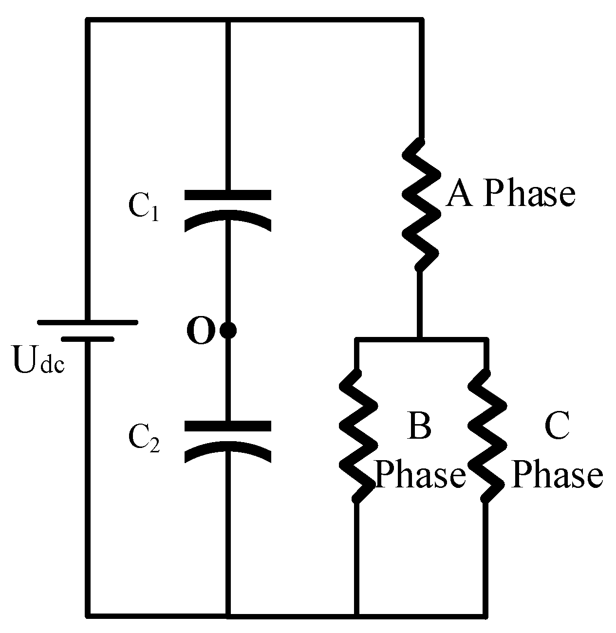
Taking the large vector PNN as an example, its corresponding equivalent circuit is shown in Figure 8. As can be seen from the Figure 8, the three-phase load is directly connected to the DC voltage source and is not connected to the midpoint of the DC-side capacitor; therefore, there will be no current flowing into or out of the midpoint, which will not affect the midpoint potential. This does not lead to the charging or discharging of the upper and lower capacitors on the DC side, thereby affecting fluctuations in the midpoint potential. Other large vectors are similar to PNN. In summary, it can be concluded that all large vectors will not affect the midpoint potential.
Taking PON, for example, of Middle Vectors, its corresponding equivalent circuit is shown in Figure 9. The direction of the current flowing towards the load is taken as the positive direction. From the figure, it can be seen that the B phase load and midpoint O form a circuit. At this point, i b is the current at the midpoint. When i b > 0 , the lower capacitor C 2 supplies power to the load and the voltage of the capacitor U C 2 decreases. At the same time, the DC source charges the upper capacitor C 1 and the voltage of the capacitor U C 1 increases. This increases the midpoint potential. When i b < 0 , the situation is opposite. In summary, it can be found that O of the switching vector affects the midpoint potential balance. The direction of current at the midpoint also affects the midpoint potential.
Taking POO and ONN as examples, the equivalent circuit of two switch states of small vectors is shown in Figure 10. As shown in the figure, the current of the midpoint in the POO is i O = i b + i c = i a . The current of the midpoint in ONN is i O = i a . The influences of these two small vectors on the midpoint potential are direct opposites of each other. In summary, small vectors do affect the midpoint potential, but they exist in pairs that exert counterbalancing effects.
Taking the zero vector OOO as an example, its switching state is as shown in Figure 11 below. It can be seen from Figure 11 that there is no current loop between the midpoint O on the DC side and the load, hence, it will not affect the midpoint potential. Other zero vectors are similar to OOO, and there is also no current loop between the midpoint and the load. In summary, zero vectors will not affect the midpoint potential.
In summary, it can be concluded that the fundamental reason for the effect on the midpoint potential balance is that there is a current flowing through the midpoint. Table 3 lists the currents at the midpoint corresponding to each medium and small vector.
In summary, there is no current at the midpoint when there is a zero vector or a large vector, so it has no effect on the balance of the midpoint potential. The medium vector affects the balance of the midpoint potential, but there are not two medium vectors that have opposite effects on the balance of the midpoint potential. Therefore, its impact is uncontrollable. There are paired vectors in small vectors that have opposite effects on the midpoint potential, so the balance of the midpoint potential can be optimized by controlling these small vectors.

2.3. The Method of Balancing Midpoint Potential

This article proposes an improved algorithm for space vectors. The voltages of the two capacitors on the DC side are measured. A regulatory factor k is proposed to control the time of the vector that affects the balance of midpoint potential. Taking the sector I region ① for example, Figure 12 is the time allocation of vector under SVPWM and NPB–RSVPWM.
Figure 12 shows the time allocation of vectors in the sector I region ①. The direction of the current flow towards the load is taken as the positive direction. When the switching vector is ONN, the current at the midpoint of the DC side is i a , and when it is POO, the current at the midpoint is i a . The adjustment factor is changed to change the action time of the two corresponding vectors by measuring the voltage of the two capacitors on the DC side.
If the average value of the midpoint’s current in a switching cycle is zero, the variation in the capacitor voltage during the switching cycle will be minimized as much as possible. In the actual operation of inverter systems, there are other disturbance factors, such as different initial values of upper and lower capacitor voltages, that cause capacitor voltage deviations. During a switching cycle, the midpoint potential should be made as balanced as possible through the feedback of introducing midpoint current/charge.
According to the order of switch vectors in sector I, a pair of small vectors with opposite effects will always be used. The action time of small vectors can be changed by adjusting the allocation factor k to achieve the balance of midpoint potential.
During the switching cycle, the voltage difference that is measured between the upper and lower capacitors on the DC side is:
Δ U C = U C 1 U C 2
At this point, the amount of charge flowing out of the midpoint should be:
Q O = C Δ U C
Taking region ① in sector I as an example, the average charge at the midpoint flowing out of the inverter during a switching cycle is:
Q a v = 2 k T a i a T c i c ( 1 2 k ) T a i a
When Q O = Q a v ,
k = T a i a + T c i c + Q O 4 T a i a
When U r e f is located in sector I region 1, the allocation factor k for the action time of the small vector is calculated through the above equation. According to this formula, the allocation factor can be used to accurately allocate the action time of small vectors in order to achieve the goal of midpoint potential balance. In order to obtain a suitable value of k, this article adopts the method described in the following text.
When the current of neutral point i o > 0 ,
(1) If U C 1 > U C 2 , Q a v < 0 is needed, the current flows into the lower capacitor C2 to charge it and balance the midpoint potential as much as possible. When Q a v < 0 , k can be expressed as:
k < T a i a + T c i c 4 T a i a
Due to 0 k 0.5 , the minimum value of k is 0. If the calculated value of k is greater than zero, then, in each cycle, k takes a value according to the following equation.
k = T a i a + T c i c 4 T a i a r a n d ( 1 )
The “rand(1)” represents randomly taking a value within 0~1.
(2) If U C 1 < U C 2 , Q a v > 0 is needed, the current flows out of the lower capacitor C2 to charge it and balance the midpoint potential as much as possible. When Q a v > 0 , k can be expressed as:
k > T a i a + T c i c 4 T a i a
Due to 0 k 0.5 , the maximum value of k is 0.5. If the calculated value of k is less than 0.5, then, in each cycle, k takes a value according to the following equation.
k = 0.5 T a i a + T c i c 4 T a i a r a n d ( 1 ) + T a i a + T c i c 4 T a i a
(3) If U C 1 = U C 2 , k = 0.25.
When i a < 0 , the formula for calculating the value of k can be derived by analogy. Other regions are also similar.

3. Simulation Verification

A simulation model of the three-phase T-type inverter is built to analyze the characteristics and performances of the proposed NPB–RSVPWM strategy, and its circuit parameters are shown in Table 4.
This article uses an FFT analysis (Fast Fourier Transform) in MATLAB 2019b signal processing tools to analyze signals and perform a spectrum analysis and feature extraction. The harmonic content at different frequencies can be obtained by analyzing the unfiltered line voltage. These data can demonstrate the effect of the NPB–RSVPWM strategy in spreading the line voltage spectrum to reduce the harmonic content at the switching frequency and its integer multiples. Compared to the traditional SVPWM strategy, the NPB–RSVPWM strategy proposed in this paper not only reduces the harmonic content at the switching frequency and its integer multiples while keeping the output voltage constant, but also optimizes the midpoint voltage imbalance situation that exists in the T-type three-level inverter. Figure 13 is output voltage waveforms under SVPWM and NPB–RSVPWM.
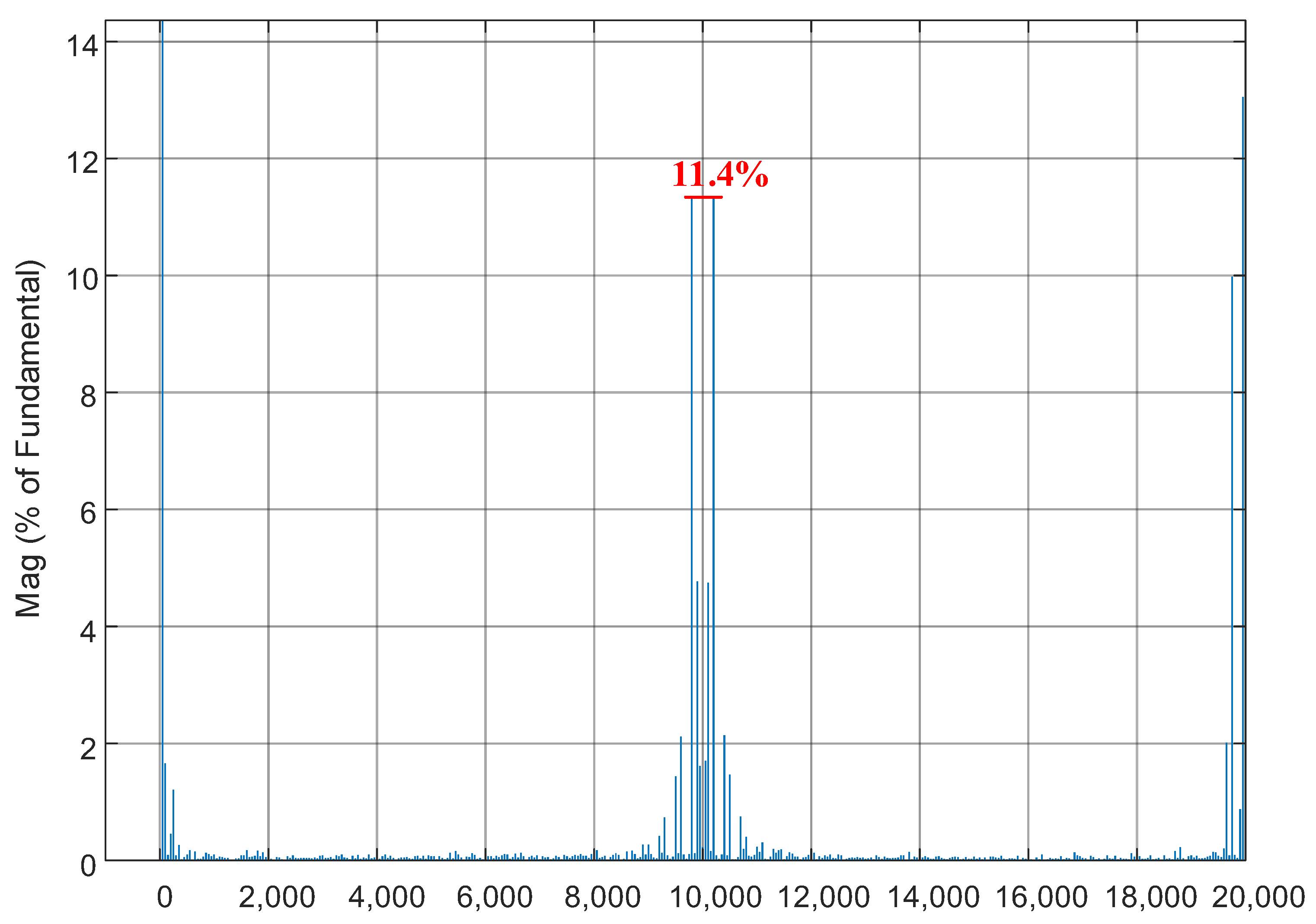
By comparing the output voltage waveforms under the two strategies, the fundamental amplitude of the output voltage is consistent. This shows that the NPB–RSVPWM strategy proposed in this article has a similar output to that of the SVPWM strategy. However, the FFT analyses of the output voltages under the two strategies reveal that the harmonic content at the switching frequency and its multiples of the output voltage under the NPB–RSVPWM strategy are effectively dispersed.
According to the simulation results, when the NPB–RSVPWM strategy is adopted, the harmonic content at the switch frequency and its multiples are significantly reduced. As can be seen from Figure 14, compared to the SVPWM strategy, the harmonic content near 10 kHz is reduced from 12.2% to 3.2%, and the highest value is reduced from 12.2% to 6.0%. In conclusion, the NPB–RSVPWM strategy proposed in this paper effectively disperses the harmonic content at the switching frequency and its integer multiples, thereby reducing the voltage noise of the inverter.
The Even Harmonic Pulse Width Modulation (EVSVPWM) strategy demonstrates a significant effect in eliminating harmonics at odd multiples of the switching frequency. Therefore, this paper conducts a comparative analysis between the output line voltage spectrum of the proposed NPB–RSVPWM strategy and the EVSVPWM strategy. In Figure 15, it can be seen that the MSVPWM strategy effectively eliminates harmonics at odd multiples, but still harbors a considerable amount of harmonic content at even multiples of the switching frequency. In contrast, the strategy studied in this paper significantly reduces the peak values of the harmonic content, which is better for reducing voltage noise.
In the T-type three-level inverter, the common-mode voltage is the voltage between the midpoint of the three-phase load and the midpoint between the two capacitors on the DC side. In the comparison between the SVPWM strategy and the NPB–RSVPWM strategy for common-mode voltage, it can be seen from Figure 16 and Figure 17 that the common-mode voltage amplitudes of both strategies are consistent. However, due to the integration of random frequency carrier technology, there are subtle differences in the waveforms.
The common-mode current is the current between the inverter output phase and the ground, represented mathematically as the vector sum of the three-phase output currents. In Figure 18 and Figure 19, it can be observed that the NPB–RSVPWM strategy proposed in this paper has an improvement effect on the fluctuation in the common-mode current.
The NPB–RSVPWM strategy proposed in this paper also has a significant effect on optimizing the midpoint balance in T-type inverters. From Figure 20, it can be clearly seen that, compared with the ordinary SVPWM strategy, the NPB–RSVPWM strategy proposed in this article has a smaller fluctuation in the midpoint potential on the DC side, and the voltage fluctuation in the capacitor on the DC side is reduced from the highest 310.3 V to 301.8 V. The blue and orange lines in Figure 20 are the voltages of the two capacitors on the DC side.

4. Experimental Verification

An experimental platform was built for the T-type three-level inverter to further verify the effectiveness and feasibility of the NPB–RSVPWM strategy. The experimental apparatus is depicted in Figure 21.
The experimental parameters of the device are as shown in Table 5:
As shown in Figure 22, it can be found that, although the strategy proposed in this paper will change the time of period, it will only have a slight impact on the details of the waveform. The amplitudes are approximately equal, all around 24 V.
By performing an FFT analysis on the output voltage under two strategies, the effect of the NPB–RSVPWM strategy proposed in this paper on dispersing harmonic energy can be clearly seen. As shown in the Figure 23, the highest harmonic content of the line voltage obtained from the experiment is 11.2% under the SVPWM strategy, while under the NPB–RSVPWM strategy, the highest harmonic content of the line voltage is only 5%. A comparison clearly shows the superiority of the strategy proposed in this paper.
Particularly within low-frequency ranges, dead time directly influences the switching angles and timing of the inverter, which can introduce additional harmonic content into the inverter’s output voltage and current waveforms. As shown in Figure 24, the experimental findings indicate that, as the dead time increases, specific low-order harmonics are significantly augmented. This finding substantiates the critical impact of dead time on harmonic distortion.
As shown in Figure 25, it can be clearly seen that the strategy proposed in this paper has no impact on the amplitude of the output voltage by comparing the output voltage after filtering. The amplitude of the line voltage under both strategies is a sine wave with a peak value of approximately 24 V by observing the line voltage output of the inverter.
By measuring the voltage on both sides of the capacitor on the DC side, the midpoint balance of the T-type inverter can be clearly seen. The experimental results under the two strategies are shown in Figure 26. When the conventional SVPWM strategy is applied, the voltage fluctuation reaches 1.8 V. However, after adopting the NPB–RSVPWM strategy proposed in this paper, the voltage fluctuation is reduced to 0.9 V, effectively improving the issue of midpoint potential imbalance.

5. Conclusions

In conclusion, this paper proposes the NPB–RSVPWM strategy to reduce the PWM voltage noise of T-type three-level inverters and optimize the midpoint potential balance on the DC side. In this strategy, the proposed random frequency and midpoint balance vector allocation methods are used, combining space vector modulation. Therefore, the NPB–RSVPWM strategy not only has an excellent output voltage harmonic performance, but it can also reduce the PWM voltage noise of the output voltage and optimize the problem of midpoint voltage imbalance on the DC side. Furthermore, compared with the NPC inverter, the T-type inverter naturally has a better waveform quality and lower PWM voltage noise. Therefore, prioritizing the T-type inverter structure along with the RSVPWM method, which rely on space vector modulation and equilibrium of the midpoint voltage, is advisable for attaining a superior waveform integrity and diminished PWM voltage disturbance. Both simulation and practical experimentations robustly affirm the proposed NPB–RSVPWM strategy’s practicality and viability in this research.
The NPB–RSVPWM strategy studied in this paper reduces voltage noise by dispersing harmonic energy, but it does not fundamentally decrease harmonic energy. Future research in this paper will explore methods for eliminating harmonics, such as interleaved parallel topologies, and will combine these with the strategy proposed in this paper to further suppress harmonics and reduce voltage noise.

Author Contributions

Conceptualization, H.W. and R.G.; methodology, H.W.; validation, H.W. and J.T.; writing—original draft preparation, H.W.; writing—review and editing, H.W., R.G. and X.W.; project administration, R.G.; funding acquisition, R.G. All authors have read and agreed to the published version of the manuscript.

Funding

This research was funded by the National Natural Science Foundation of China, grant number: 61561007, and the Natural Science Foundation of Guangxi Province, China, grant number: 2017GXNSFAA198168.

Data Availability Statement

The data used to support the findings of the study are available within the article.

Conflicts of Interest

The authors declare no conflicts of interest.

References

  1. Wen, H.; Xiao, W.; Wen, X.; Armstrong, P. Analysis and Evaluation of DC-Link Capacitors for High-Power-Density Electric Vehicle Drive Systems. IEEE Trans. Veh. Technol. 2012, 61, 2950–2964. [Google Scholar]
  2. Binojkumar, A.C.; Saritha, B.; Narayanan, G. Acoustic Noise Characterization of Space Vector Modulated Induction Motor Drives—An Experimental Approach. IEEE Trans. Ind. Electron. 2014, 62, 3362–3371. [Google Scholar] [CrossRef]
  3. Le Besnerais, J.; Lanfranchi, V.; Hecquet, M.; Brochet, P. Characterization and Reduction of Audible Magnetic Noise Due to PWM Supply in Induction Machines. IEEE Trans. Ind. Electron. 2010, 57, 1288–1295. [Google Scholar] [CrossRef]
  4. Liang, W.; Luk, P.C.-K.; Fei, W. Analytical Investigation of Sideband Electromagnetic Vibration in Integral-Slot PMSM Drive With SVPWM Technique. IEEE Trans. Power Electron. 2017, 32, 4785–4795. [Google Scholar] [CrossRef]
  5. Liang, W.; Wang, J.; Luk, P.C.-K.; Fang, W.; Fei, W. Analytical Modeling of Current Harmonic Components in PMSM Drive With Voltage-Source Inverter by SVPWM Technique. IEEE Trans. Energy Convers. 2014, 29, 673–680. [Google Scholar] [CrossRef]
  6. Sekhar, K.R.; Srinivas, S. Torque ripple reduction PWMs for a single DC source powered dual-inverter fed open-end winding induction motor drive. IET Power Electron. 2018, 11, 43–51. [Google Scholar] [CrossRef]
  7. von Jouanne, A.; Rendusara, D.; Enjeti, P.; Gray, J. Filtering techniques to minimize the effect of long motor leads on PWM inverter-fed AC motor drive systems. IEEE Trans. Ind. Appl. 1996, 32, 919–926. [Google Scholar] [CrossRef]
  8. Liu, S.; Liu, C. Virtual-vector-based robust predictive current control for dual three-phase PMSM. IEEE Trans. Ind. Electron. 2021, 68, 2048–2058. [Google Scholar] [CrossRef]
  9. Lee, K.; Shen, G.; Yao, W.; Lu, Z. Performance characterization of random pulse width modulation algorithms in industrial and commercial adjustable-speed drives. IEEE Trans. Ind. Appl. 2017, 53, 1078–1108. [Google Scholar] [CrossRef]
  10. Kumar, A.B.C.; Narayanan, G. Variable-switching frequency PWM technique for induction motor drive to spread acoustic noise spectrum with reduced current ripple. IEEE Trans. Ind. Appl. 2016, 52, 3927–3938. [Google Scholar] [CrossRef]
  11. Jia, Y.; Wang, X.; Mao, L.; Yang, S.; Zhang, H. Application and simulation of SVM in three phase inverter. In Proceedings of the 2011 6th International Forum on Strategic Technology (IFOST), Harbin, China, 22–24 August 2011; Volume 1, pp. 541–544. [Google Scholar]
  12. Huang, Y.; Xu, Y.; Li, Y.; Yang, G.; Zou, J. PWM frequency voltage noise cancellation in three-phase VSI using the novel SVPWM strategy. IEEE Trans. Power Electron. 2018, 33, 8596–8606. [Google Scholar] [CrossRef]
  13. Peyghambari, A.; Dastfan, A.; Ahmadyfard, A. Selective voltage noise cancellation in three-phase inverter using random SVPWM. IEEE Trans. Power Electron. 2016, 31, 4604–4610. [Google Scholar] [CrossRef]
  14. Huang, Y.; Xu, Y.; Zhang, W.; Zou, J. Hybrid RPWM technique based on modified SVPWM to reduce the PWM acoustic noise. IEEE Trans. Power Electron. 2019, 34, 5667–5674. [Google Scholar] [CrossRef]
  15. Davis, T.T.; Gajare, P.M.; Dey, A. A novel floating capacitor voltage control technique for 9-level T-type inverter with reduced device count. In Proceedings of the IECON 2019—45th Annual Conference of the IEEE Industrial Electronics Society, Lisbon, Portugal, 14–17 October 2019; pp. 1526–1531. [Google Scholar]
  16. Muduli, U.R.; Behera, R.K. A Modified High Gain Boost TNPC Inverter with Neutral Point Balancing for Three-phase Induction Motor Driven Electric Vehicle. In Proceedings of the 2020 IEEE International Conference on Power Electronics, Drives and Energy Systems (PEDES), Jaipur, India, 16–19 December 2020; pp. 1–6. [Google Scholar]
  17. Man, Y.K.; Bian, C.Y.; Xu, N.; Zhu, Z.Q. Influence of zero space vector and PWM switching frequency on acoustic noise induction motors. J. Northeast. Univ. (Nat. Sci.) 2002, 23, 738–741. [Google Scholar]
  18. Peng, H.; Yuan, Z.; Narayanasamy, B.; Zhao, X.; Deshpande, A.; Luo, F. Comprehensive analysis of three-phase three-level T-type neutral-point clamped inverter with hybrid switch combination. In Proceedings of the IEEE 10th International Symposium on Power Electronics for Distributed Generation Systems (PEDG), Xi’an, China, 3–6 June 2019; pp. 816–821. [Google Scholar]
  19. Liu, J.; Zhang, J.; Li, H. A T-type NPC three-level three-phase four-arm midpoint potential control strategy. J. Electr. Power Sources 2016, 14, 68–73. [Google Scholar]
  20. Li, W.; Feng, J.; Wang, C. Dead zone-free carrier cascade PWM control of TNPC inverter. J. Syst. Simul. 2016, 28, 1628–1636. [Google Scholar]
  21. Wang, S.; Yang, S.; Li, Y.; Xie, Z. Inverter common mode voltage suppression method based on virtual space vector overmodulation strategy. Electr. Power Autom. Equip. 2022, 42, 76–81+96. [Google Scholar]
  22. Siwakoti, Y.P.; Peng, F.Z.; Blaabjerg, F.; Loh, P.C.; Town, G.E. Impedance-Source Networks for Electric Power Conversion Part I: A Topological Review. IEEE Trans. Power Electron. 2015, 30, 699–716. [Google Scholar] [CrossRef]
  23. Stankovic, A.M.; Verghese, G.E.; Perreault, D.J. Analysis and synthesis of randomized modulation schemes for power converters. IEEE Trans. Power Electron. 1995, 10, 680–693. [Google Scholar] [CrossRef]
  24. Boudouda, A.; Boudjerda, N.; Melit, M.; Nekhoul, B.; El Khamlichi Drissi, K.; Kerroum, K. Optimized RPWM technique for a Variable Speed Drive using induction motor. In Proceedings of the International Symposium on Electromagnetic Compatibility—EMC EUROPE, Rome, Italy, 17–21 September 2012; pp. 1–6. [Google Scholar]
  25. Paramasivan, M.; Paulraj, M.M.; Balasubramanian, S. Assorted carrier-variable frequency-random PWM scheme for voltage source inverter. IET Power Electron. 2017, 10, 444–460. [Google Scholar] [CrossRef]
Figure 1. Topology of the T-type three-level inverter.
Electronics 13 01656 g001
Figure 2. Fixed frequency modulation.
Electronics 13 01656 g002
Figure 3. Overall technical framework of the NPB–RSVPWM strategy.
Electronics 13 01656 g003
Figure 4. Diagram of I-sector.
Electronics 13 01656 g004
Figure 5. (a) Vector state of region 1 and (b) status of A-phase’s switches.
Electronics 13 01656 g005
Figure 6. Diagram of time allocation.
Electronics 13 01656 g006
Figure 7. Diagram of random frequency carrier and fixed frequency carrier.
Electronics 13 01656 g007
Figure 8. Diagram of PNN equivalent circuit.
Electronics 13 01656 g008
Figure 9. Diagram of PON equivalent circuit.
Electronics 13 01656 g009
Figure 10. (a) Diagram of POO equivalent circuit and (b) diagram of ONN equivalent circuit.
Electronics 13 01656 g010
Figure 11. Diagram of OOO equivalent circuit.
Electronics 13 01656 g011
Figure 12. (a) Time allocation of vector (SVPWM) and (b) time allocation of vector (NPB–RSVPWM).
Electronics 13 01656 g012
Figure 13. Diagram of output voltage waveforms under SVPWM and NPB–RSVPWM.
Electronics 13 01656 g013
Figure 14. Diagram of output voltages’ FFT analysis under SVPWM and NPB–RSVPWM.
Electronics 13 01656 g014
Figure 15. FFT analysis of output voltage under EVSVPWM.
Electronics 13 01656 g015
Figure 16. Diagram of common-mode voltage under NPB–RSVPWM.
Electronics 13 01656 g016
Figure 17. Diagram of common-mode voltage under SVPWM.
Electronics 13 01656 g017
Figure 18. Diagram of common-mode current under SVPWM.
Electronics 13 01656 g018
Figure 19. Diagram of common-mode current under NPB–RSVPWM.
Electronics 13 01656 g019
Figure 20. Comparison chart of midpoint potential.
Electronics 13 01656 g020
Figure 21. Diagram of experimental device.
Electronics 13 01656 g021
Figure 22. Diagram of output line voltages under SVPWM and NPB–RSVPWM.
Electronics 13 01656 g022
Figure 23. (a) The spectrum diagram of SVPWM output voltage and (b) the spectrum diagram of NPB–RSVPWM output voltage.
Electronics 13 01656 g023
Figure 24. (a) The spectrum diagram of output voltage (dead time = t) and (b) the spectrum diagram of output voltage (dead time = 2 t).
Electronics 13 01656 g024
Figure 25. Diagram of output line voltages after filtering under SVPWM and NPB–RSVPWM.
Electronics 13 01656 g025
Figure 26. (a) The voltage of capacitor C1 (SVPWM) and (b) The voltage of capacitor C1 (NPB–RSVPWM).
Electronics 13 01656 g026
Table 1. Table of the vector vertices’ coordinates.
Vector VertexCoordinate
O(0, 0)
A ( 1 3 U dc , 0)
B ( 1 6 U dc ,   3 6 U dc )
C ( 2 3 U dc , 0)
D ( 1 2 U dc ,   3 6 U dc )
E ( 1 3 U dc ,   3 3 U dc )
Table 2. Order of the vector state.
RegionOrder of the Vector State
1ONN OON OOO POO OOO OON ONN
2OON OOO POO PPO POO OOO OON
3ONN OON PON POO PON OON ONN
4OON PON POO PPO POO PON OON
5ONN PNN PON POO PON PNN ONN
6OON PON PPN PPO PPN PON OON
Table 3. Vector corresponds to the current at the midpoint.
Small Vector i O Small Vector i O Middle Vector i O
OON i a POO i a PON i b
PPO i c OON i c OPN i a
NON i b OPO i b NPO i c
OPP i a NOO i a NOP i b
NNO i c OOP i c ONP i a
POP i b ONO i b PNO i c
Table 4. The table of simulation parameters.
ParameterValueParameterValue
DC voltage600 VCarrier frequency7.5–10 kHz
Capacitance value5 µFSampling frequency20 kHz
Modulation ratio0.9Three-phase load10 Ω
Table 5. The table of experimental parameters.
ParameterValueParameterValue
DC voltage24 VCarrier frequency7.5–10 kHz
Capacitance value5 µFSampling frequency20 kHz
Modulation ratio0.9Three-phase load10 Ω
Disclaimer/Publisher’s Note: The statements, opinions and data contained in all publications are solely those of the individual author(s) and contributor(s) and not of MDPI and/or the editor(s). MDPI and/or the editor(s) disclaim responsibility for any injury to people or property resulting from any ideas, methods, instructions or products referred to in the content.