Abstract
In this study, we designed a wideband CMOS power amplifier to support multi-band and multi-standard wireless communications. First, an input matching technique through LC network and a wideband design technique using a low Q-factor transformer were proposed. In addition, a design technique was proposed to improve output matching using RC feedback. To verify the feasibility of the proposed design methodology for wideband CMOS power amplifiers, the designed power amplifier was fabricated using a 180 nm RFCMOS process. The size including all of the matching network and test pads was 1.38 × 0.90 mm2. In addition, the effectiveness of the proposed power amplifier was verified through the measured results using modulated signals of WCDMA, LTE, and 802.11n WLAN.
1. Introduction
With the continuous development of wireless mobile communications, several generations of communication technologies are being introduced. Accordingly, the wireless terminal is equipped with various wireless communication components to support multi-band and multi-standard [1,2,3]. In addition, in order to increase the usage time of the battery, the capacity of the battery is continuously increasing. In other words, considering the limited volume of the wireless terminals, the need for miniaturization of the wireless components continues to be required despite supporting multi-band and multi-standard. Hence, in order to miniaturize wireless components at the same time as supporting multi-band and multi-standard in a wireless terminal, one wireless component should be capable of supporting multi-band and multi-standard [4,5,6,7].
For wireless components capable of supporting such multi-band and multi-standard, design techniques to secure the wideband characteristics of high-frequency circuits are essential [8,9,10]. In particular, in the case of power amplifiers dealing with high output power, securing high output power and wideband characteristics at the same time is one of the challenges [11]. Currently, widely known design techniques for wideband power amplifiers include a distributed amplifier, a Darlington amplifier, and tunable matching network structures.
In the case of a distributed amplifier structure, the advantage is that it is easy to secure an operating frequency band through a relatively simple structure [12,13,14]. However, one problem is that the size of the entire power amplifier increases due to a structurally required transmission line or inductance. The increased area of the power amplifier with the distributed structure acts as an unfavorable factor in terms of the miniaturization of the wireless communication terminal.
In the case of the Darlington structure, as a technique that secures wideband through simple changes in the transistor constituting the amplifier, the increase in the area of the amplifier is relatively suppressed [15,16]. However, the theoretical basis for securing wideband in the Darlington structure is mainly suitable for amplifiers dealing with small signals, and one problem is that additional design techniques are required to apply it to power amplifiers dealing with relatively large signals.
Tunable matching network techniques change the configuration of the matching circuit using switches [17,18,19]. Through this, a multi-band may be secured by securing a configuration of a matching circuit suitable for various frequency bands through switches. However, considering the high output power of the power amplifier, power consumption by switches for the reconfiguration of the matching circuit may deteriorate the efficiency of the entire power amplifier.
As a result, multiple power amplifiers are typically used to support multi-bands. In addition, although there are cases where the multi-band is supported by a single power amplifier, in this case, the frequency bands constituting the multi-band are mostly adjacent to each other. However, in this study, a design technique was proposed to support frequency bands that are not adjacent to each other with a single power amplifier.
In this study, input and output matching circuit design techniques for compact size wideband power amplifiers were proposed. A design technique for configuring a wideband matching circuit with LC structures using a low quality-factor (Q-factor) transformer was proposed for the input matching circuit. In the output matching circuit, a technique for simultaneously achieving wideband power matching and wideband conjugate matching using an RC-feedback structure along with a low Q-factor transformer was proposed. In order to verify the feasibility of the proposed design technique, a power amplifier operating from 0.9 GHz to 2.4 GHz was designed using a 180 nm RFCMOS process.
2. Design of the Wideband Input Matching Network
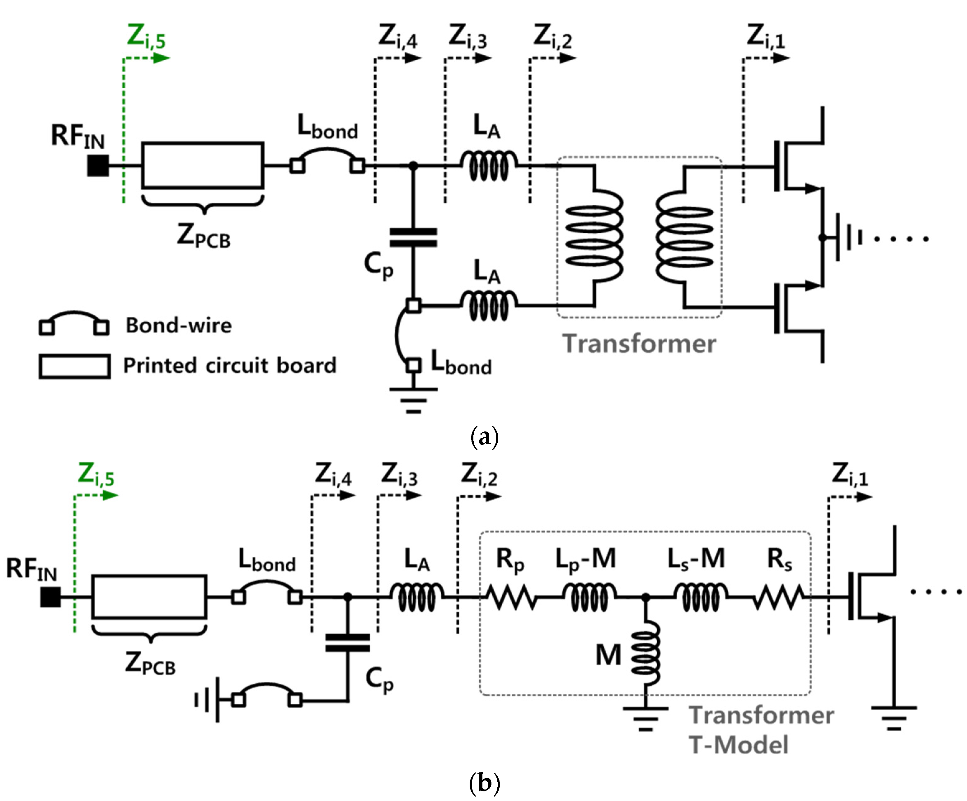
In this study, the LC network structure was adapted for a wideband conjugate matching to the input matching circuit. In general, the LC network structure for wideband has a problem in that the area of the entire circuit increases due to the size of the bulky inductors. In this study, an input transformer was used to solve these problems and convert a single-ended signal into a differential signal. Figure 1a shows an input matching circuit using a transformer. The input matching circuit consists of a transformer serving as a balun, an additional inductor, LA, a capacitor for matching, CP, a bonding wire, Lbond, and ZPCB, a transmission line implemented on PCB. At this time, if the input transformer is represented as a T-mode, the input matching circuit becomes an L-C-L structure as shown in Figure 1b.
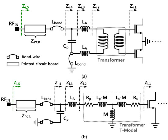
Figure 1.
The proposed input matching circuit: (a) schematic and (b) equivalent circuit.
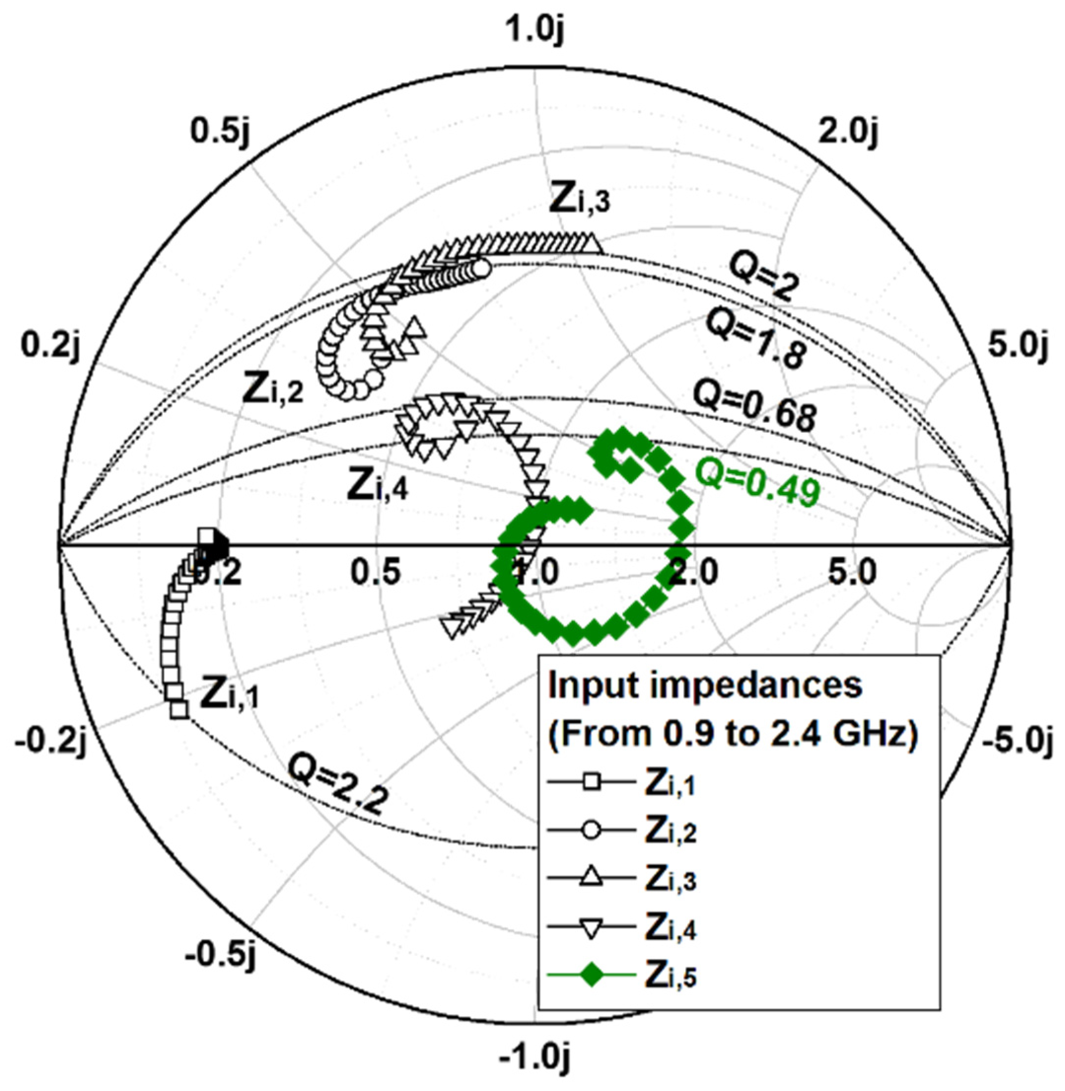
First, as shown in Figure 2, Zi,1, the input impedance of the used transistor, is shown in the Smith chart. Here, the frequency band was set from 0.9 GHz to 2.4 GHz. The Zi,1s at 0.9 GHz, 1.8 GHz, and 2.4 GHz were 5.12 − j10.85 Ω, 10.05 − j0.27 Ω, and 9.20 − j0.65 Ω, respectively. As shown in Figure 2, for Zi,1, the value of the constant Q-line was 2.2. Therefore, for wideband input matchings, the input matching circuit was configured so that the constant Q-line did not exceed 2.2 during the input matching process. As can be seen in Figure 1b, Zi,2 by the input transformer, Zi,3 by LA, and Zi,4 by CP all had a constant Q-line of less than 2.2. To this end, the input transformer was designed to have a low Q-factor. The outmost size of the input transformer was 0.60 × 0.22 mm2, and the minimum and maximum values of the parasitic inductance of the primary winding in the frequency range from 0.9 GHz to 2.4 GHz were 2.5 nH and 2.8 nH, respectively. On the other hand, the minimum and maximum values of the parasitic inductance of secondary winding were 4.6 nH and 5.4 nH, respectively. In addition, the minimum and maximum Q-factors of the input transformer were 5.3 at 1.7 GHz and 6.9 at 0.9 GHz, respectively.
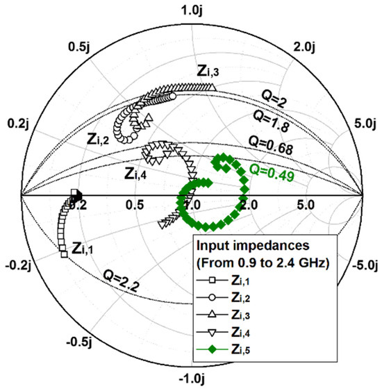
Figure 2.
Simulated input impedance of the input matching circuit.
The designed LA and CP used for the purpose of tuning the input matching circuit were 0.4 nH and 2.7 pF, respectively. Finally, Zi,5 by Lbond and ZPCB became the input impedance of the entire power amplifier, and it can be seen that wideband input matching was completed, as shown in Figure 2.
3. Design of the Wideband Output Matching Network
The output matching of the power amplifier should be carefully designed compared to the input matching. Since the output impedance of the power amplifier has a direct relationship with the output power, it is generally designed using a power matching technique, which entails the deterioration of S22.
In general, it is well known that the RC-feedback technique improves the stability and bandwidth of an amplifier. However, in this study, RC feedback was used not only to improve the stability and bandwidth of the power amplifier but also to improve S22 [20,21]. First, output power was secured using the power matching technique; then, S22 was secured through RC feedback. Here, in the feedback, an inductor may be used instead of a resistor, but a resistor was used to minimize the chip area.
3.1. Design of the Wideband Power Matching Network
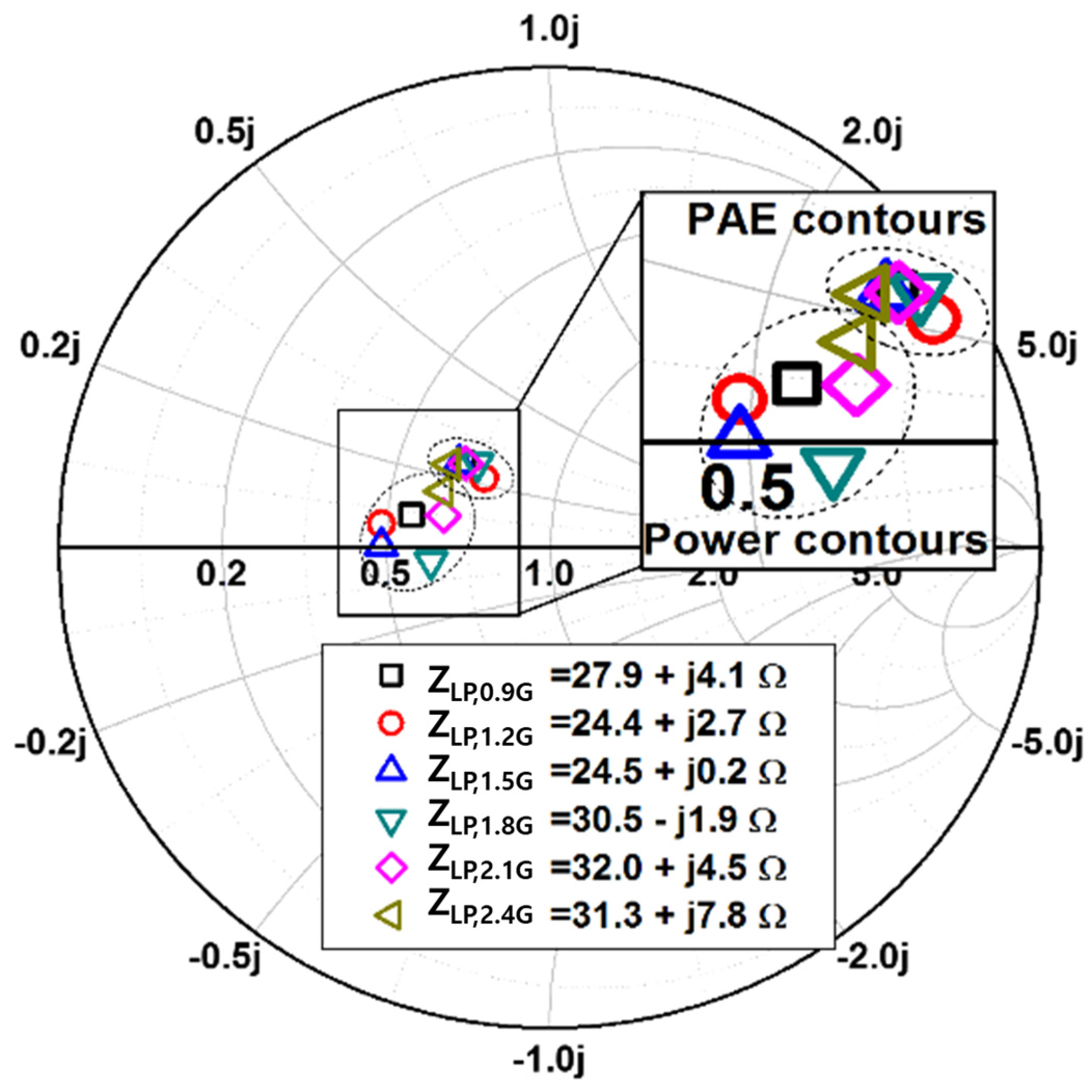
First, the load-pull simulation, which is essential for power matching, was performed. Figure 3 shows the impedance for maximum power and maximum efficiency per frequency of the transistor constituting the differential power amplifier as a result of the load-pull simulation. The load-pull simulation was performed in the frequency range from 0.9 GHz to 2.4 GHz. The impedances for maximum power were 27.9 + j4.2 Ω, 30.55 − j1.9 Ω, and 31.35 + 7.80 Ω at 0.9 GHz, 1.8 GHz, and 2.4 GHz, respectively. There was a need to design a matching circuit capable of converting 50 Ω, which is a load impedance, into an impedance for maximum power and maximum efficiency per frequency.
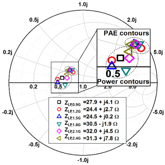
Figure 3.
Results of the load-pull simulation of the designed power amplifier.
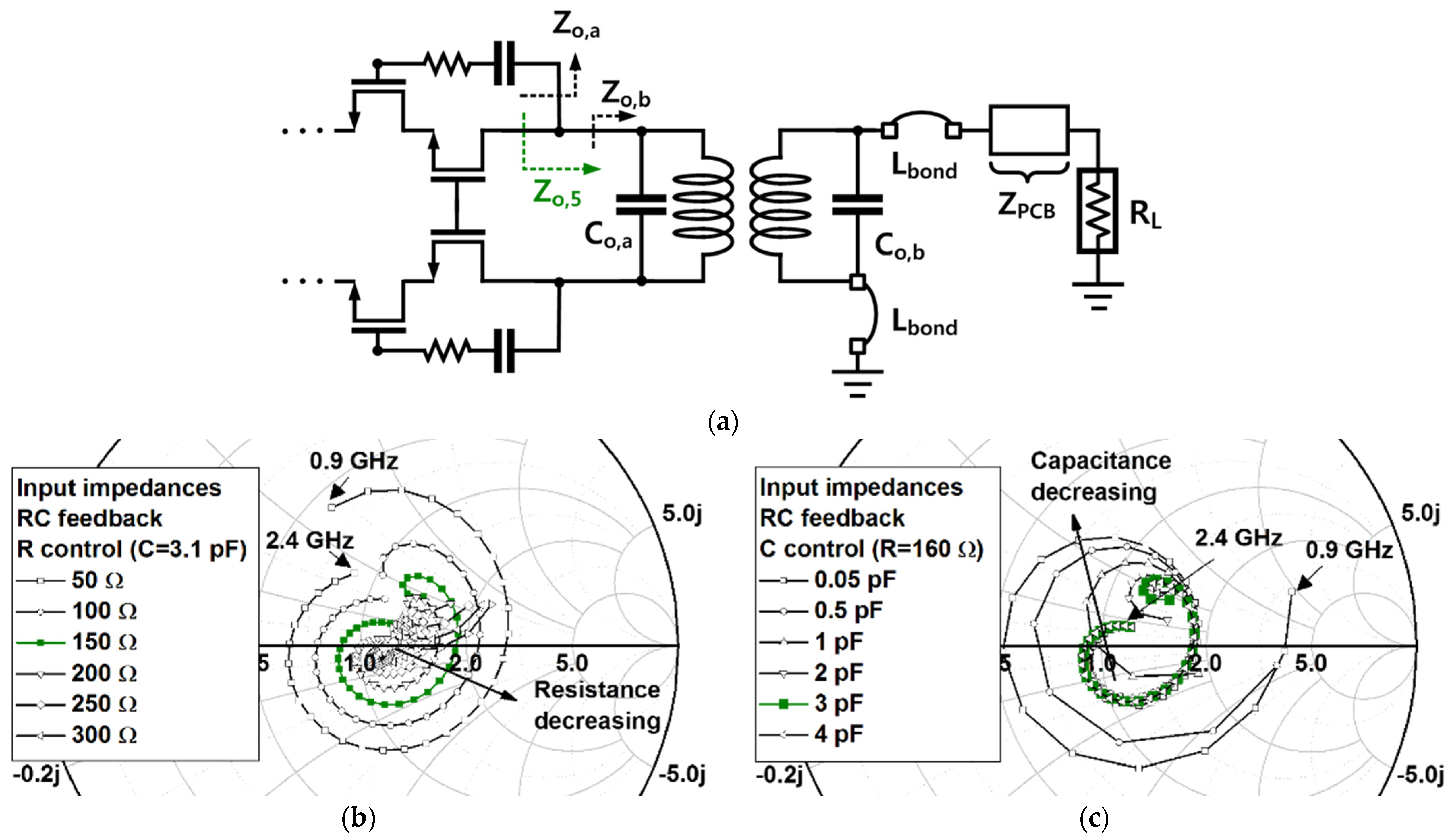
In this study, a power matching technique was performed based on the output matching circuit shown in Figure 4a. The output matching circuit consisted of ZPCB, which is a transmission line on a PCB, and Lbond, which is the parasitic inductance of the bonder wire, capacitors, and an output transformer. Zo,1 was set to 50 Ω. In the frequency range from 0.9 GHz to 2.4 GHz, the minimum and maximum values of the parasitic inductance of the primary winding of the output transformer were 5.96 nH and 7.60 nH, respectively. The minimum and maximum values of the parasitic inductance of the secondary winding were 6.35 nH and 8.61 nH, respectively. Co,a and Co,b are metal–insulator–metal (MIM) capacitors and were used to tune the output matching circuit.
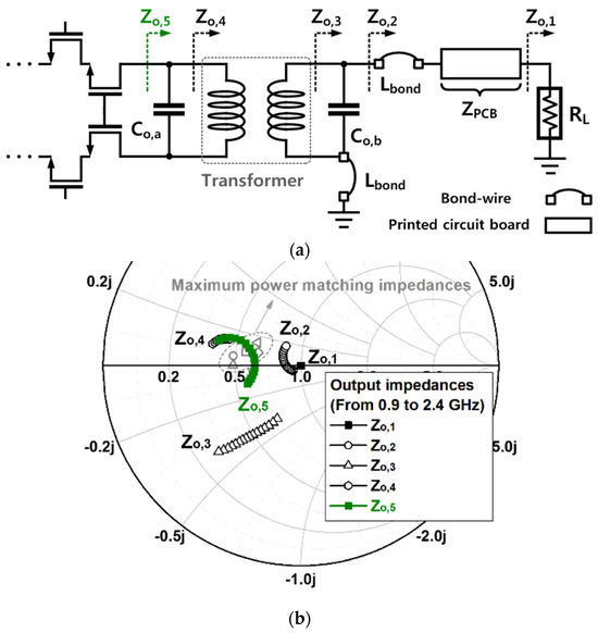
Figure 4.
Load-pull simulations for power amplifier: (a) schematic and (b) results.
3.2. Design of the Wideband Conjugate Matching Network
In this study, an RC-feedback technique was used to secure a wideband conjugate matching without deterioration of power matching. As shown in Figure 5a, the RC-feedback technique was applied between the input and output of the cascode structure. At this time, as shown in Figure 5, looking at Zo,a while varying the R and C values, it can be seen that Zo,a was successfully varied according to the R and C values.
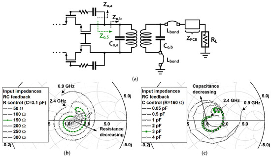
Figure 5.
Variations in the simulated impedance of the RC feedback, according to variations in the R and C values: (a) schematic, (b) variation in R value, and (c) variation in C value.
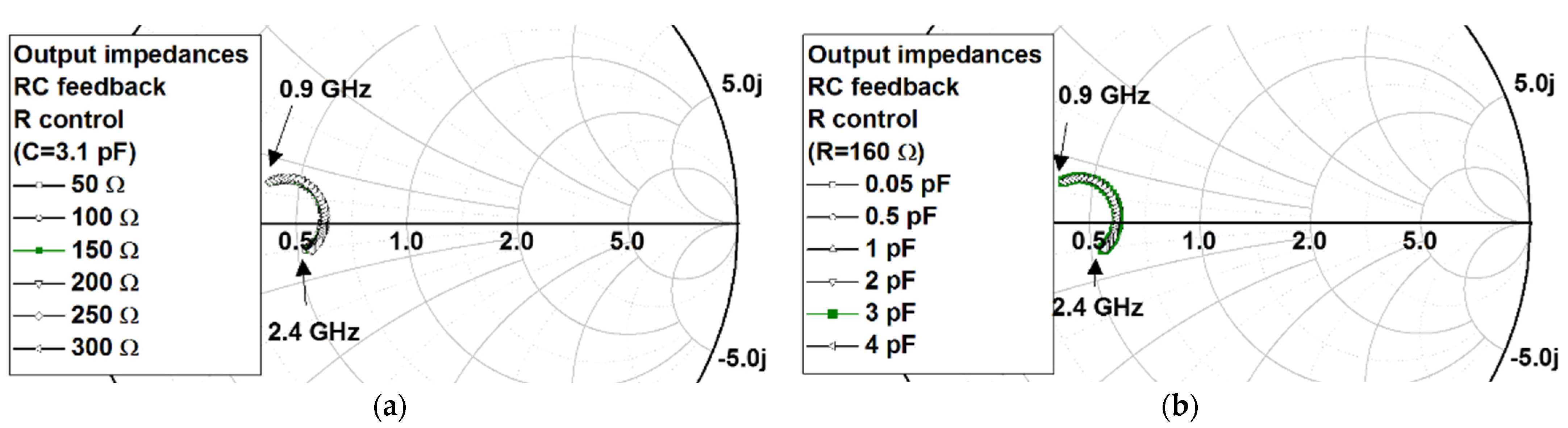
In general, the impedances of R and C used for the RC feedback were relatively high compared to the optimal impedances by the load-pull simulation. Therefore, as shown in Figure 6, even when the R and C values of the RC feedback changed, Zo,5 was almost the same as Zo,b. This means that even when the RC-feedback technique was applied, the impedance for power matching according to load-pull simulations was maintained.
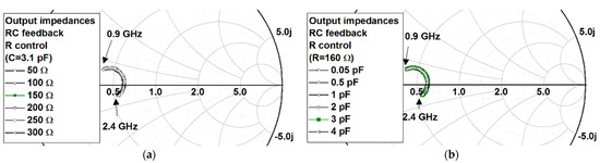
Figure 6.
Variation in the simulated input impedance of the output matching circuit according to variations in the R and C values: (a) variation in the R value and (b) variation in the C value.
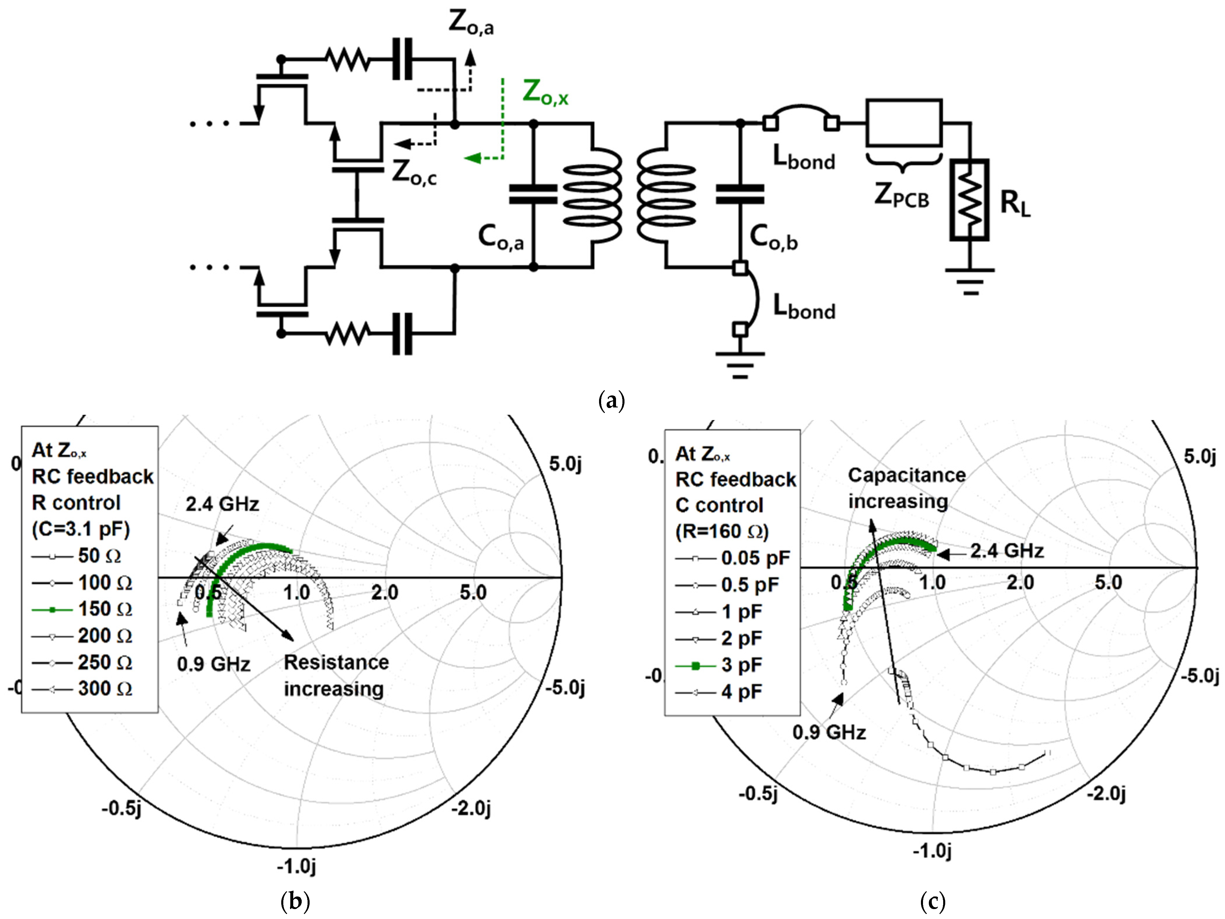
On the other hand, Figure 7 shows the simulation results examining the output impedance of the amplification stage according to the RC feedback. As can be seen from Figure 7, Zo,x varied according to the variation in the R and C values of the RC feedback.
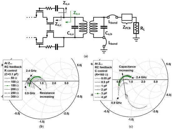
Figure 7.
Variation in the simulated output impedance of the amplification stage according to variations in the R and C values: (a) schematic, (b) variation in the R value, and (c) variation in the C value.
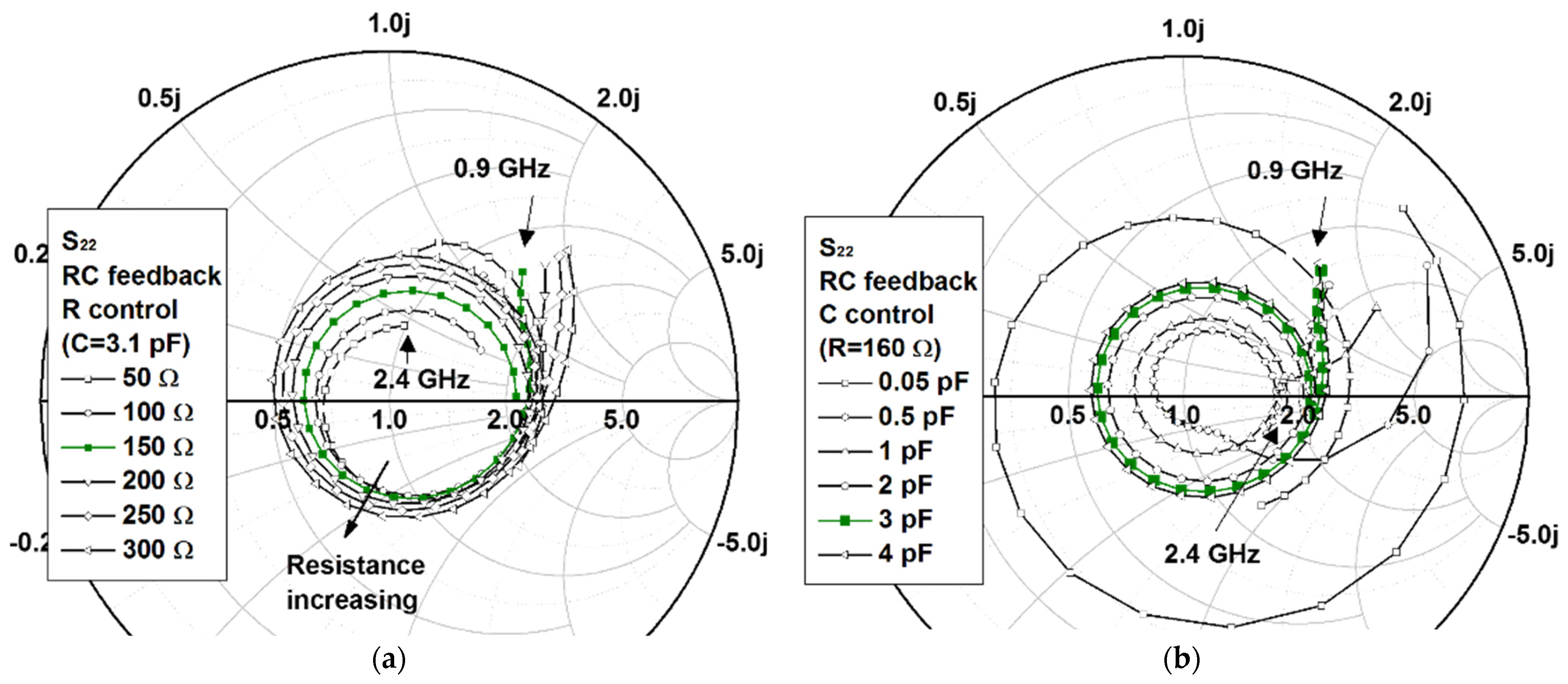
Consequently, from Figure 6 and Figure 7, when the RC-feedback technique is used, the conjugate matching can be optimized without deteriorating the power matching. As shown in Figure 8, it is possible to optimize the S22 of the power amplifier by optimizing the R and C values of the RC feedback. In this study, the R and C values of the RC feedback were set to 150 Ω and 3 pF to secure wideband conjugate matching.
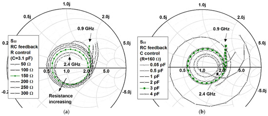
Figure 8.
Variation in the simulated S22 of the power amplifier according to variations in the R and C values: (a) variation in the R value and (b) variation in the C value.
4. Design Results of the Proposed CMOS Power Amplifier
In order to verify the effectiveness of the proposed design methodology, a power amplifier operating from 0.9 GHz to 2.4 GHz was designed using a 180 nm RFCMOS process. The amplifier was designed as a single stage with a differential structure, and input and output transformers were used. In addition, it was designed in a cascode structure to overcome the low breakdown voltage of CMOS, and the supply voltage was 3.3 V. Figure 9 presents the schematic of the designed power amplifier, and the values of the used devices are summarized in Table 1.
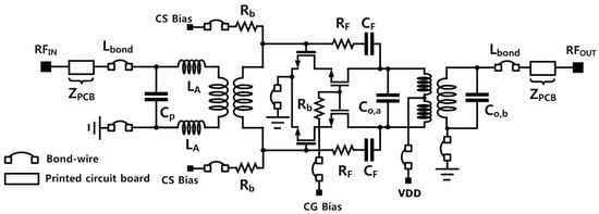
Figure 9.
Schematic of the designed CMOS power amplifier.

Table 1.
Size of the used transistors, inductors, and capacitors.
Figure 10 shows a chip photograph of the fabricated power amplifier. The sizes of the input and output transformers were 0.60 × 0.22 mm2 and 0.70 × 0.45 mm2, respectively. The overall size of the power amplifier chip including the test pads was 1.38 × 0.90 mm2.
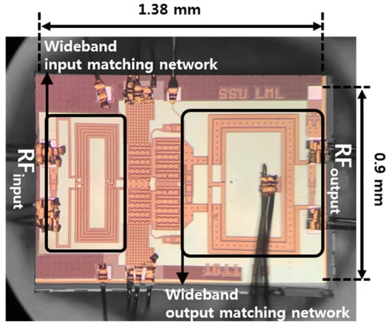
Figure 10.
Chip photograph of the designed power amplifier.
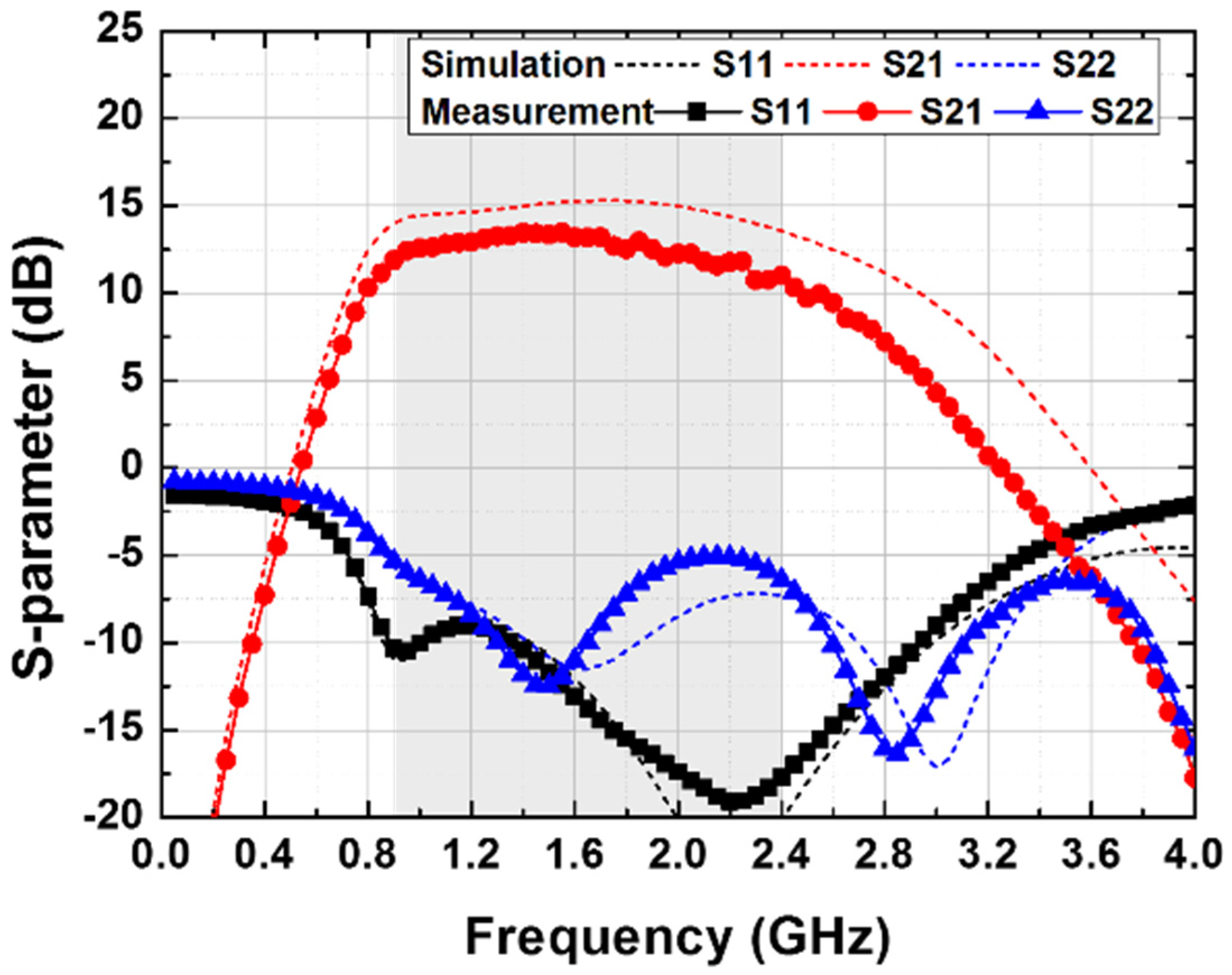
Figure 11 shows the measured results of the S-parameters. The measured S11, S22, and S21 at 1.8 GHz were −18.8 dB, −9.4 dB, and 12.5 dB, respectively. The measured S11, S22, and S21 at 2.4 GHz were −16.0 dB, −6.3 dB, and 10.2 dB, respectively. The 3 dB bandwidth was measured as approximately 1.5 GHz at a 1.5 GHz center frequency, in which case the fractional bandwidth was 90.9%. As shown in Figure 11, the measurement results of the S22 were somewhat deteriorated compared to the simulation results. This was expected due to the fact that the errors in the electromagnetic (EM) simulation accuracy for interconnection lines on PCB and integrated circuit and parasitic components that were not considered.

Figure 11.
Measured S-parameters of the designed CMOS power amplifier.
The following are measurement results using modulation signals of WCDMA, LTE, and WLAN to verify the effectiveness of multi-standard support.
4.1. Measurement Results with WCDMA Modulated Signal
First, when a WCDMA modulated signal with a 5 MHz bandwidth was used, the performance of the proposed power amplifier was measured.
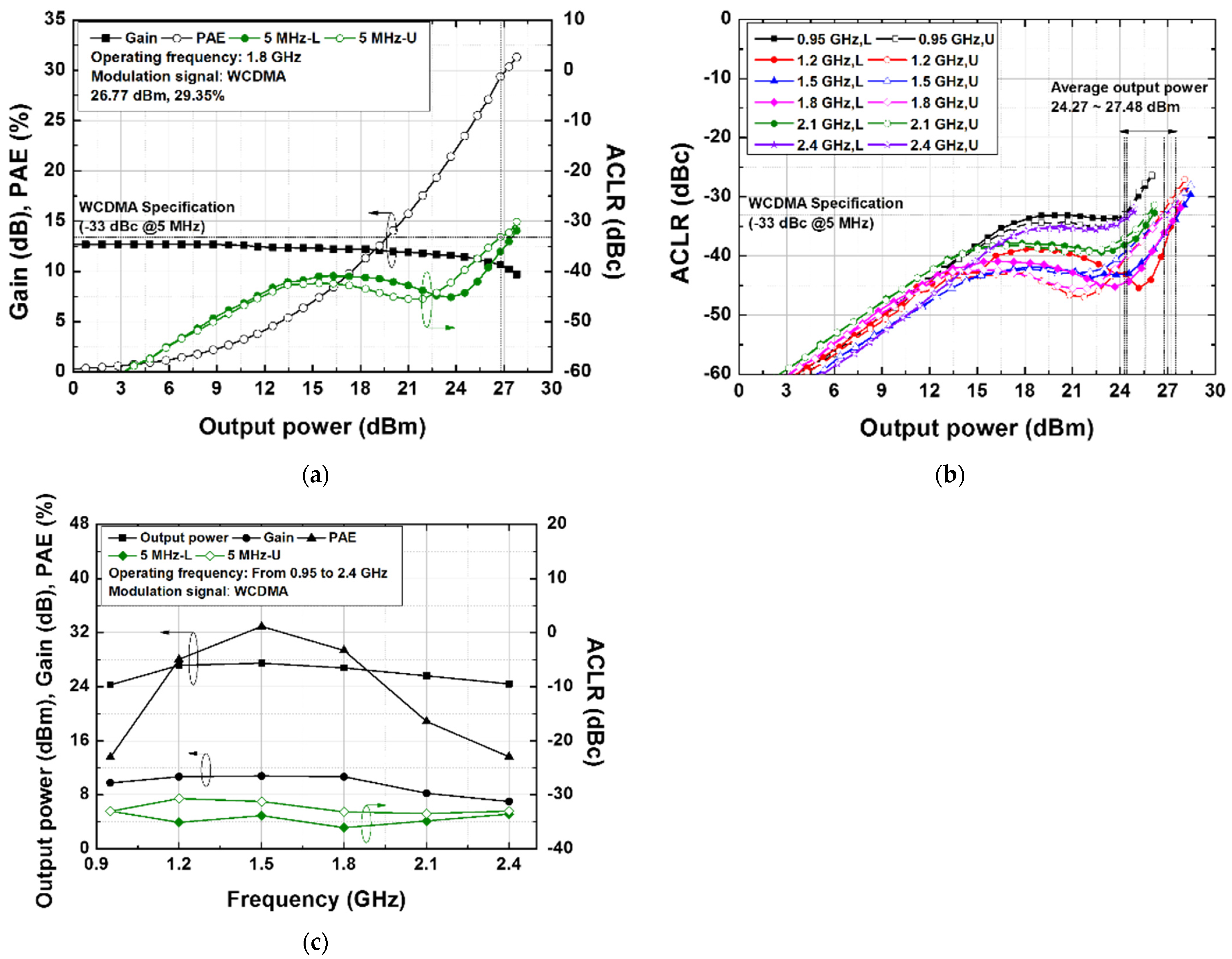
As shown in Figure 12a, when the 1.8 GHz WCDMA signal was input, the maximum linear output power that satisfies the ACLR of −33 dBc was measured as 26.77 dBm, and the PAE was measured as 29.35%. Figure 12b shows the measurement results of the ACLR according to the output power in the operating frequency range from 0.95 GHz to 2.40 GHz. Under conditions where the ACLR was less than −33 dBc, the output power was measured in the range of 24.27 dBm to 27.48 dBm. Figure 12c shows the measurement results of the output power, gain, PAE, and ACLR according to the operating frequency.
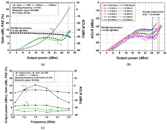
Figure 12.
Measurement results with a 5 MHz bandwidth WCDMA modulated signal: (a) gain, PAE, and ACLR at 1.8 GHz, (b) ACLR according to output power, and (c) output power, gain, PAE, and ACLR, according to the operating frequency.
4.2. Measurement Results with LTE Modulated Signal
When an LTE modulated signal with a 10/20 MHz bandwidth was used, the performance of the proposed power amplifier was measured as shown in Figure 13.
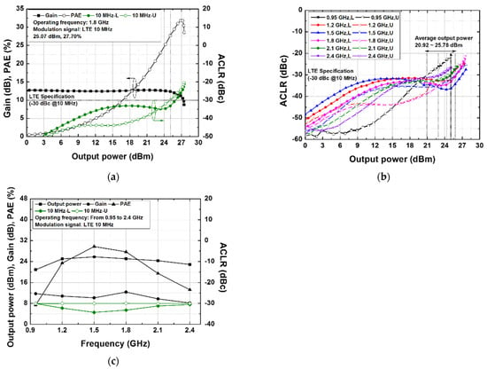
Figure 13.
Measurement results with a 10 MHz bandwidth LTE modulated signal: (a) gain, PAE, and ACLR at 1.8 GHz, (b) ACLR according to output power, and (c) output power, gain, PAE, and ACLR, according to the operating frequency.
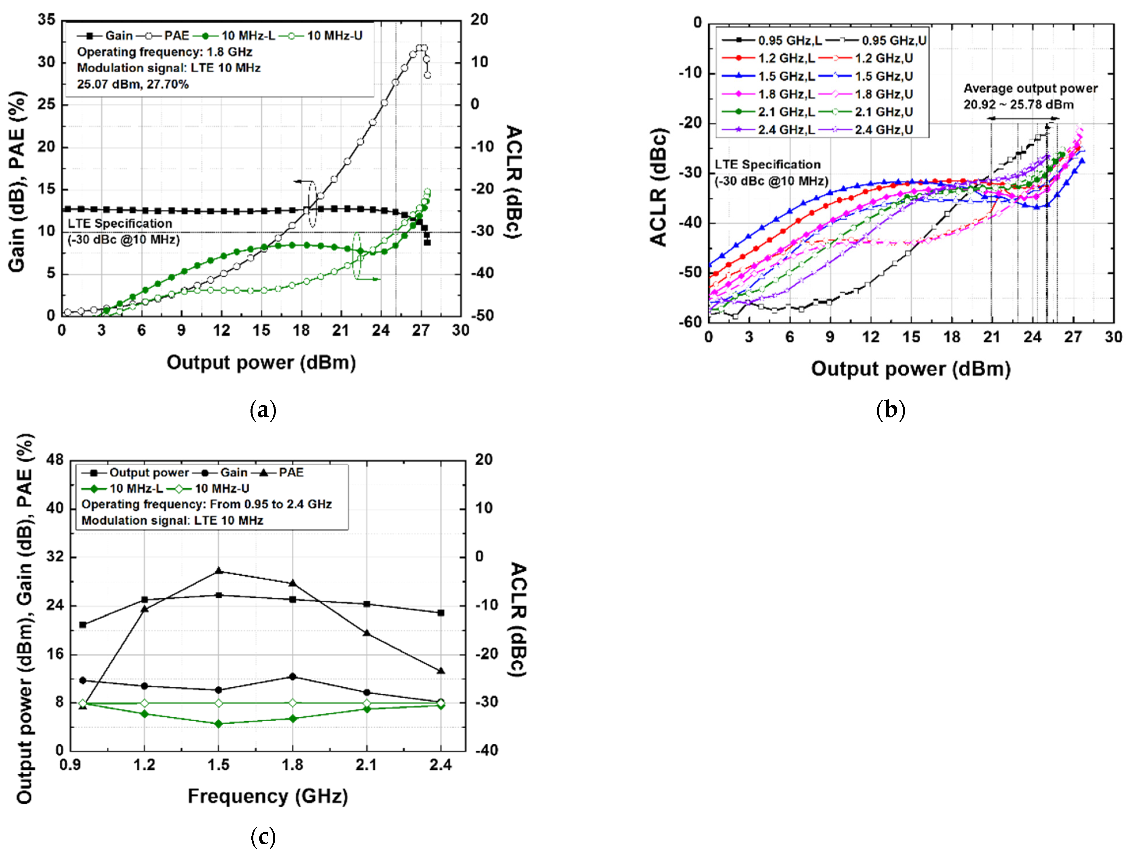
As shown in Figure 13a, when the 10 MHz bandwidth LTE signal at a center frequency of 1.8 GHz was input, the maximum linear output power that satisfies the ACLR of −30 dBc was measured as 25.07 dBm, and the PAE was measured as 27.70%. Figure 13b shows the measurement results of ACLR with a 10 MHz bandwidth LTE signal according to the output power in the operating frequency range from 0.95 GHz to 2.40 GHz. Under conditions where the ACLR was less than −30 dBc, the output power was measured in the range of 20.92 dBm to 25.78 dBm. Figure 13c shows the measurement results of the output power, gain, PAE, and ACLR with a 10 MHz bandwidth LTE signal, according to the operating frequency.
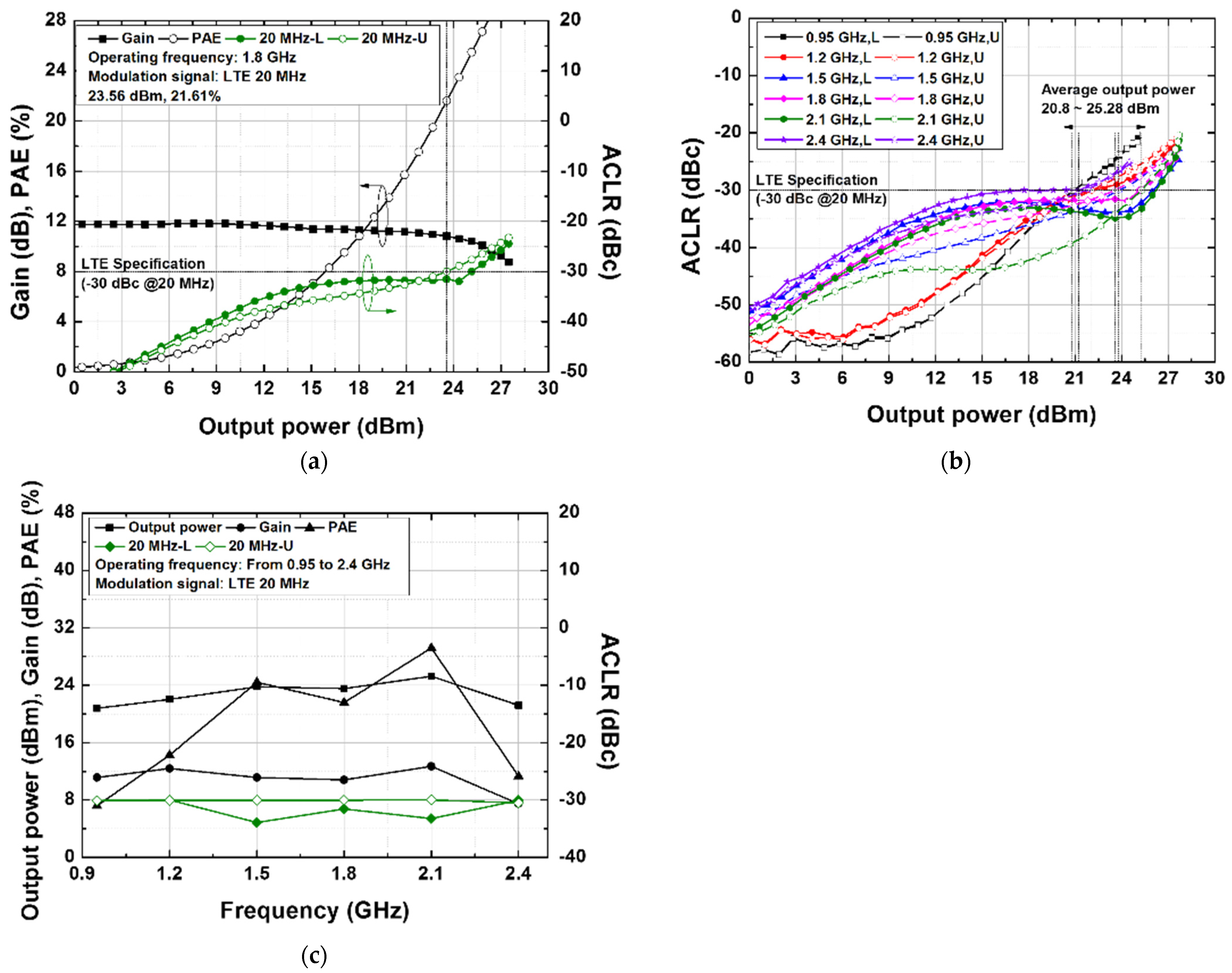
As shown in Figure 14a, when the 20 MHz bandwidth LTE signal at center frequency of 1.8 GHz was input, the maximum linear output power that satisfies the ACLR of −30 dBc was measured as 23.56 dBm, and the PAE was measured as 21.61%. Figure 14b shows the measurement results of ACLR with a 20 MHz bandwidth LTE signal according to the output power in the operating frequency range from 0.95 GHz to 2.40 GHz. Under conditions where the ACLR was less than −30 dBc, the output power was measured in the range of 20.80 dBm to 25.28 dBm. Figure 14c shows the measurement results of the output power, gain, PAE, and ACLR with 20 MHz bandwidth LTE signal, according to the operating frequency.
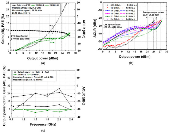
Figure 14.
Measurement results with a 20 MHz bandwidth LTE modulated signal: (a) gain, PAE, and ACLR at 1.8 GHz, (b) ACLR according to output power, and (c) output power, gain, PAE, and ACLR, according to the operating frequency.
4.3. Measurement Results with a WLAN Modulated Signal
When a 64 QAM 802.11n WLAN modulated signal with 2.4 GHz operating frequency was used, the performance of the proposed power amplifier was measured.
As shown in Figure 15a, when the 64 QAM 802.11n WLAN signal at a center frequency of 2.4 GHz was input, the maximum linear output power that satisfied the EVM of 3.98% was measured as 21.00 dBm, and the PAE was measured as 14.40%. Figure 15b shows the measurement results of ACLR with a 64 QAM 802.11n WLAN signal according to the output power in the operating frequency range from 0.95 GHz to 2.40 GHz. Under conditions where the EVM was less than 3.98%, the output power was measured in the range of 20.92 dBm to 25.78 dBm. Figure 15c shows the measurement results of the output power, gain, PAE, and EVM with a 64 QAM 802.11n WLAN signal, according to the operating frequency.
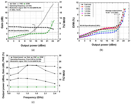
Figure 15.
Measurement results with a 64 QAM 802.11n WLAN modulated signal: (a) gain and EVM at 2.4 GHz, (b) EVM according to output power, and (c) output power, gain, PAE, and EVM, according to the operating frequency.
The performance of the multi-band CMOS power amplifier is summarized and compared with various CMOS power amplifier in Table 2. As shown in Table 2, the power amplifier of this study occupied the small chip area, but the multi-band performance was comparable.
Table 2.
Comparison of state-of-the-art CMOS multi-band power amplifiers.
5. Conclusions
In this study, we proposed a wideband power amplifier using a 180 nm RFCMOS process. The proposed wideband power amplifier operates from 1.0 GHz to 2.4 GHz without using additional circuits and switches through the proposed input and output matching circuits. To verify the proposed matching techniques, we measured the performance of the fabricated CMOS power amplifier using WCDMA, LTE, and WLAN modulated signals. The measured performance of the designed dual-band power amplifier was 27.3 dBm linear output power and 32.3% PAE with the WCDMA modulated signal at 1.8 GHz. With a 10 MHz (20 MHz) bandwidth LTE modulated signal, the measured linear output power and PAE were 25.8 dBm (23.8 dBm) and 28.64% (23.00%), respectively. In addition, with a 64 QAM 802.11n WLAN modulated signal at the 2.4 GHz center frequency, the measured linear output power and PAE were 21.10 dBm and 15.00%, respectively.
Author Contributions
Conceptualization, M.L. and C.P.; methodology, M.L., J.Y. and C.P.; investigation, M.L., J.Y. and J.L.; supervision, C.P.; writing—original draft, M.L. and J.L.; review and editing C.P. All authors have read and agreed to the published version of the manuscript.
Funding
This work was supported by the National Research Foundation of Korea (NRF) through the Korea Government (MSIT) under Grant NRF-2021R1A2C1013666.
Data Availability Statement
All the data used in the study are provided in the article.
Conflicts of Interest
The authors declare no conflicts of interest.
References
- Zhang, Y.; Mueller, J.H.; Mohr, B.; Liao, L.; Atac, A.; Wunderlich, R.; Heinen, S. A Multi-Frequency Multi-Standard Wideband Fractional-N PLL with Adaptive Phase-Noise Cancellation for Low-Power Short-Range Standards. IEEE Trans. Microw. Theory Tech. 2016, 64, 1133–1142. [Google Scholar] [CrossRef]
- Fehri, B.; Boumaiza, S.; Sich, E. Crest Factor Reduction of Inter-Band Multi-Standard Carrier Aggregated Signals. IEEE Trans. Microw. Theory Tech. 2014, 62, 3286–3297. [Google Scholar] [CrossRef]
- Jain, S.; Jang, S.-L.; Tchamov, N.T. Tuned LC-Resonator Dual-Band VCO. IEEE Microw. Wirel. Compon. Lett. 2016, 26, 204–206. [Google Scholar] [CrossRef]
- Xie, C.; Wu, P.; Tan, C.; Yuan, Y.; Zeng, J.; Yu, Z. An X/Ku Dual-Band Switchless Frequency Reconfigurable GaAs Power Amplifier. IEEE Microw. Wirel. Compon. Lett. 2022, 32, 539–542. [Google Scholar] [CrossRef]
- Lee, W.; Hong, S. Frequency-Reconfigurable SP4T Switch with Plaid Metal Transistors and Forward Body Biasing for Enhanced RON × COFF Characteristics. IEEE Trans. Circuits Syst. II Express Briefs 2022, 69, 399–403. [Google Scholar] [CrossRef]
- Kanchetla, V.K.; Kharalkar, A.; Jain, S.; Khyalia, S.K.; Joy, J.; Jose, S.; Zele, R. A Compact, Reconfigurable CMOS RF Receiver for NavIC/GPS/Galileo/BeiDou. IEEE Trans. Microw. Theory Tech. 2022, 70, 3361–3373. [Google Scholar] [CrossRef]
- Ko, B.; Lee, S.; Seo, W.; Sim, T.; Kim, S.; Kim, M.-S.; Kim, J. A 39/48 GHz Switchless Reconfigurable Low Noise Amplifier Using Common Gate and Coupled-Line-Based Diplexer. IEEE Trans. Circuits Syst. II Express Briefs 2023, 70, 4028–4032. [Google Scholar] [CrossRef]
- Wang, Z.; Wang, X.; Liu, Y. A Wideband Power Amplifier in 65 nm CMOS Covering 25.8 GHz–36.9 GHz by Staggering Tuned MCRs. Electronics 2023, 12, 3566. [Google Scholar] [CrossRef]
- Mauludin, M.F.; Lee, D.-H.; Kim, J. A Wideband Low-Power Balun-LNA with Feedback and Current Reuse Technique. Electronics 2022, 11, 1372. [Google Scholar] [CrossRef]
- Mahmood, H.U.; Utomo, D.R.; Han, S.-K.; Kim, J.; Lee, S.-G. A Ku-Band RF Front-End Employing Broadband Impedance Matching with 3.5 dB NF and 21 dB Conversion Gain in 45-nm CMOS Technology. Electronics 2020, 9, 539. [Google Scholar] [CrossRef]
- Lee, M.; Park, C. A Triple-Band CMOS Power Amplifier Using Multi-Band and Switchable Matching Network for Wireless Mobile. IEEE Trans. Microw. Theory Tech. 2019, 67, 4220–4231. [Google Scholar] [CrossRef]
- Kim, J. A Wideband Triple-Stacked CMOS Distributed Power Amplifier Using Double Inductive Peaking. IEEE Microw. Wirel. Compon. Lett. 2019, 29, 787–790. [Google Scholar] [CrossRef]
- Alizadeh, A.; Medi, A. Distributed Class-J Power Amplifiers. IEEE Trans. Microw. Theory Tech. 2017, 65, 513–521. [Google Scholar] [CrossRef]
- Chirala, M.K.; Guan, X.; Nguyen, C. Integrated Multilayered On-Chip Inductors for Compact CMOS RFICs and Their Use in a Miniature Distributed Low-Noise-Amplifier Design for Ultra-Wideband Applications. IEEE Trans. Microw. Theory Tech. 2008, 56, 1783–1789. [Google Scholar] [CrossRef]
- Kilinc, S.; Yarman, B.S.; Ozoguz, S. Broadband Power Amplifier Design via Fictitious Matching. IEEE Trans. Circuits Syst. II Express Briefs 2022, 69, 4844–4848. [Google Scholar] [CrossRef]
- Kim, M.-S.; Jhon, H. A Broadband Gain Amplifier Designed with the Models for Package and Diode Using 0.5 μm GaAs E-pHEMT Process. Electronics 2021, 10, 2678. [Google Scholar] [CrossRef]
- Zhai, C.; Liu, H.-Y.; Cheng, K.-K.M. Single-Chip CMOS Reconfigurable Dual-Band Tri-Mode High-Efficiency RF Amplifier Design. IEEE Trans. Circuits Syst. II Express Briefs 2021, 68, 868–872. [Google Scholar] [CrossRef]
- Kang, L.; Chen, W.; Wu, A. A Reconfigurable S-/X-Band GaN MMIC Power Amplifier. IEEE Microw. Wirel. Compon. Lett. 2022, 32, 547–550. [Google Scholar] [CrossRef]
- Aggrawal, E.; Rawat, K. Reconfigurable Chireix Outphasing Power Amplifier Over Multiple Frequency Bands. IEEE Trans. Circuits Syst. II Express Briefs 2020, 67, 1019–1023. [Google Scholar] [CrossRef]
- Su, G.; Sun, L.; Wen, J.; Wang, H.; Yu, Z.; Zhang, N. An estimable stability method applied to power amplifier design. In Proceedings of the 2011 IEEE Electrical Design of Advanced Packaging and Systems Symposium (EDAPS), Hanzhou, China, 12–14 December 2011; pp. 1–4. [Google Scholar] [CrossRef]
- Rasmi, A.; Marzuki, A.; Ismail, M.A.; Rahim, A.I.A.; Yahya, M.R.; Mat, A.F.A. 0.5 µm GaAs PHEMT medium power amplifier design using simple RC feedback amplifier for wireless LAN applications. In Proceedings of the 2008 Asia-Pacific Microwave Conference, Hong Kong, China, 16–20 December 2008; pp. 1–4. [Google Scholar] [CrossRef]
- Kim, B.; Lee, D.-H.; Hong, S.; Park, M. A multi-band CMOS power amplifier using reconfigurable adaptive power cell technique. IEEE Microw. Wirel. Compon. Lett. 2016, 26, 616–618. [Google Scholar] [CrossRef]
- Kim, K.; Ko, J.; Lee, S.; Nam, S. A two-stage broadband fully integrated CMOS linear power amplifier for LTE applications. IEEE Trans. Circuits Syst. II Express Briefs 2016, 63, 533–537. [Google Scholar] [CrossRef]
- Park, J.; Lee, C.; Park, C. A quad-band CMOS linear power amplifier for EDGE applications using an anti-phase method to enhance its linearity. IEEE Trans. Circuits Syst. I Regul. Pap. 2017, 64, 765–776. [Google Scholar] [CrossRef]
- Lee, M.-L.; Liou, C.-Y.; Tsai, W.-T.; Lou, C.-Y.; Hsu, H.-L.; Mao, S.-G. Fully monolithic BiCMOS reconfigurable power amplifier for multi-mode and multi-band applications. IEEE Trans. Microw. Theory Tech. 2015, 63, 614–624. [Google Scholar] [CrossRef]


Disclaimer/Publisher’s Note: The statements, opinions and data contained in all publications are solely those of the individual author(s) and contributor(s) and not of MDPI and/or the editor(s). MDPI and/or the editor(s) disclaim responsibility for any injury to people or property resulting from any ideas, methods, instructions or products referred to in the content. |
© 2024 by the authors. Licensee MDPI, Basel, Switzerland. This article is an open access article distributed under the terms and conditions of the Creative Commons Attribution (CC BY) license (https://creativecommons.org/licenses/by/4.0/).