Article

A Low-Voltage Self-Starting Boost Converter Using MPPT with Pulse Multiplication for Energy Harvesting

1
School of Optical-Electrical and Computer Engineering, University of Shanghai for Science and Technology, Shanghai 200093, China
2
214 Institute of China North Industries, Suzhou 215004, China
3
School of Physics and Information Science, Shaanxi University of Science and Technology, Xi’an 710021, China
*
Author to whom correspondence should be addressed.
Electronics 2024, 13(9), 1713; https://doi.org/10.3390/electronics13091713
Submission received: 24 March 2024 / Revised: 19 April 2024 / Accepted: 26 April 2024 / Published: 29 April 2024
(This article belongs to the Special Issue Micro Energy Harvesters: Modelling, Design, and Applications)

Abstract

:
A single-inductor, low-voltage, three-step self-starting boost converter is proposed for photovoltaic (PV) energy harvesting. In order to enhance energy transfer efficiency, a variable-step Perturb and Observe (P&O) Maximum Power Point Tracking (MPPT) scheme has been devised based on a novel pulse multiplication technique. Upon overcoming the speed and accuracy limitations, the maximum power point (MPP) of the PV model is accurately tracked. In the boost converter, the average inductor current is utilized to implement closed-loop control of the MPPT loop, enhancing the stability of the tracking process and enabling efficient energy transmission. Finally, the boost converter is implemented using a 0.18 μm CMOS process, which is capable of self-starting and maintaining stable operations at input voltages ranging from 90 mV to 300 mV, achieving a peak efficiency of 93%.

1. Introduction

With the rapid development of Internet-of-Things (IoT) technology in recent years [1,2], the proliferation of wearable devices and wireless sensors [3] for preventive medicine and continuous vital sign monitoring has surged [4,5,6], marking a trend towards increased integration. Energy harvesting technology enables the conversion of various forms of energy, such as thermal [7], solar [8], and radio frequency [9], into electrical power, thereby providing a continuous and stable energy supply for these devices. Solar energy is favored due to its abundant distribution in nature, highest power density [10], and relatively stable energy, facilitating its relatively simple harvesting and integration. However, in more integrated application scenarios, centimeter-scale photovoltaic (PV) modules can only provide milliwatt or even microwatt-level energy, with their open-circuit output voltage measuring only a few hundred millivolts. Photovoltaic cells are influenced by ambient temperature and solar irradiance [11], resulting in a non-linear relationship between output power and voltage. Consequently, a maximum power point (MPP) exists during the operation of the PV element. In order to achieve the most efficient transmission of energy, the impedance matching of maximum power point tracking (MPPT) technology further reduces the input voltage of the DC–DC boost converter, which makes efficient power conversion particularly challenging.
For PV modules with an open-circuit voltage of around 90–300 mV or even lower, the output voltage is insufficient to drive the MOS tube for energy harvesting as it falls below the threshold voltage of the MOSFET in the energy harvesting circuit. To enable self-starting energy harvesting at such low open-circuit voltage levels, various starting circuits have been proposed [12,13,14]. Inductive switching-type DC–DC converters are favored for their higher energy transmission efficiency [15]. Consequently, several architectures based on boost converters have been proposed to address the challenge of low-voltage self-starting. A Hartley oscillator structure is utilized for enabling low-voltage self-starting when the open-circuit output voltage of the energy conversion device is as low as 60 mV [16]. However, this configuration necessitates the assistance of an external inductor element to initiate circuit start-up, which poses challenges for integration. Conversely, the boost converter, relying on a single inductor, achieves low-voltage self-start at a marginally lower voltage of 57 mV [17]. Nonetheless, to address the issue of threshold MOSFET switch conduction voltage drop, a low-threshold MOS device is employed. However, the absence of MPPT technology restricts the energy transmission efficiency to a maximum of 40%.
To achieve maximum transmission efficiency of PV energy, various MPPT algorithms have been successively proposed. Among them, although the fractional open-circuit method [18] boasts a simple structure, it can only track the operating point near the MPP rather than the true maximum power operating point. Conversely, the short-circuit current method [19] necessitates short-circuiting the PV module for a period, resulting in energy loss during this interval, rendering it unsuitable for microwatt or even milliwatt-level energy supply equipment. Furthermore, the conductance incremental method [20], due to its circuit complexity and higher power consumption, is ill-suited for IoT systems requiring micro-energy harvesting. The perturb and observe (P&O) method’s [21] ability to accurately track the MPP has a relatively simple circuit structure that is easy to implement, exhibiting moderate power consumption. As a result, a widespread application for P&O algorithm is carried out in PV energy harvesting systems. Nonetheless, this algorithm is influenced by the magnitude of the disturbance voltage, impacting the tracking accuracy and speed of the system. A larger disturbance voltage results in faster tracking speed but diminishes tracking accuracy, potentially leading to oscillation near the MPP and consequent energy wastage.
With the novel pulse multiplication technique, a variable step-size P&O MPPT circuit is proposed in this paper. The step size can be dynamically adjusted to meet the requirements for tracking speed and accuracy during the energy harvesting process, enabling the most efficient transmission of energy. Furthermore, a three-step low-voltage self-starting DC–DC boost converter structure is designed, allowing the system to self-start at low PV output voltage.
The rest of this paper is organized as follows. In Section 2, the architecture and operation principles of PV energy harvesting are introduced. Specific circuit implementation details are provided in Section 3. In Section 4, the experimental results are presented and discussed, and a brief conclusion is provided in Section 5.

2. Architecture and Operation Principles for PV Energy Harvesting

The architecture of the PV energy harvesting system proposed in this article is shown in Figure 1. A three-step low-voltage self-start mechanism based on a single inductor and a variable-step P&O MPPT boost converter utilizing a novel pulse multiplication technique is designed. In order to expedite the start-up process and enhance energy harvesting efficiency, a variable-step P&O MPPT module employing an inductor average current closed-loop control is integrated into the boost converter structure. The component enclosed in the black dotted box within Figure 1 is implemented within the chip, while the blue dotted box denotes the cold start module of the system. Once the start-up process is completed, the MPPT module initiates operation, ensuring that the entire energy harvesting process operates at MPP, thereby achieving efficient energy transfer.

2.1. Three-Step Low-Voltage Self-Starting Design

In order to achieve low-voltage self-starting and maintain efficient energy harvesting during steady-state operation, the start-up process of the energy harvesting system is designed as three consecutive steps: boost converter start-up preprocessing, boost converter auxiliary path enablement, and MPPT enablement.
The distinguishing features of these stages are the specific values of the output voltage VC of the charge pump and the output voltage VOUT of the energy harvesting system. When the voltage detection circuit detects that the output voltage VC of the charge pump reaches 500 mV, it signifies the completion of the first stage, indicating that boost converter start-up preprocessing has been accomplished. Similarly, when the voltage detection circuit detects that the VOUT output reaches 1 V, it indicates the completion of the second start-up stage, namely, the enabling of the boost converter’s auxiliary path. Subsequently, the system transitions to the third stage, where MPPT is enabled. The three stages of the self-starting energy harvesting system are illustrated in Figure 2.
In order to rapidly initiate the system under low-voltage conditions and achieve maximum energy transfer efficiency, the previous structure relying on switched capacitor voltage multipliers, charge pumps, and voltage multipliers to boost the initial output voltage of energy components has been abandoned due to limitations in conversion efficiency. A three-step starting process is designed in this paper, which achieves a balanced compromise between low-voltage self-starting and energy conversion efficiency. During the cold start process, as illustrated in Figure 2a, an auxiliary starting power transistor MA with a smaller width-to-length ratio is employed to facilitate rapid initiation. However, given that the output voltage of the PV module is substantially lower than the turn-on threshold voltage of the auxiliary power transistor MA, a low-voltage ring oscillator and gate cross-coupled charge pump are utilized to augment the initial output voltage. Specifically, a low-voltage ring oscillator generates dual clock signals to drive the gate cross-coupled charge pump while enhancing its load capacity. The voltage detection circuit, triggered when the input voltage VIN gradually rises to 500 mV, is employed to detect the VC voltage. Simultaneously, the pulse signal VPULSE is generated via the voltage pulse trigger, regulating the activation and deactivation of the auxiliary power transistor. When VPULSE is high, MA is switched on, initiating the charging of the inductor L by the PV module, thereby signifying the completion of the first step.
The second step of start-up, illustrated in Figure 2b, commences with the activation of the auxiliary start-up path of the boost converter. At the falling edge of VPULSE, the magnetically induced overshoot voltage of inductor L triggers the conduction of the auxiliary rectifier diode MD, leading to the discharge of inductor L through MD. Meanwhile, the capacitor CA designated for auxiliary starting undergoes charging, and after several VPULSE pulses, VA reaches 500 mV. Upon detection by the voltage detector that VA exceeds 500 mV, the oscillator (OSC) initiates the generation of a clock signal with a large duty cycle to drive the switching power transistor Mn. As VA increases, the supply voltage of OSC gradually rises, enhancing its capability to drive Mn and accelerating the system start-up speed. Concurrently, the EN signal transitions from 0 to 1, deactivating the low-voltage ring oscillator and gate cross-coupled charge pump. Subsequently, the voltage pulse trigger is also disabled, signifying the conclusion of the second step.
In the third step, depicted in Figure 2c, upon triggering the OSC, switch S2 is closed, and rectifier MP initiates operation. Subsequently, the inductor current begins to charge the load capacitor. When the voltage detector detects that VOUT exceeds 1 V, switch S3 is closed to short-circuit capacitor CA and load capacitor CL. At this point, other modules, such as MPPT, also commence operation, transitioning the circuit into a closed-loop working mode. With this, the start-up process concludes, and the system begins steady energy harvesting at the MPP.

2.2. MPPT Control Loop and Small Signal Model

In order to achieve MPPT tracking stably, closed-loop control is essential. In a PV energy harvesting system utilizing a DC–DC converter, the variation in photovoltaic current aligns with the modulation of the duty cycle in the power switching signal governing the DC–DC converter. Hence, boost converters utilizing current mode control are highly suitable for MPPT in PV energy harvesting. To mitigate rapid tracking far from the MPP and prevent oscillation near it, this paper proposes a variable-step P&O algorithm based on a novel pulse multiplication technique. Through small-signal modeling of the boost converter based on variable-step P&O MPPT, the transfer function between the inductor current and the duty cycle of the boost converter switch control signal is derived. This facilitates the design of the MPPT control loop.
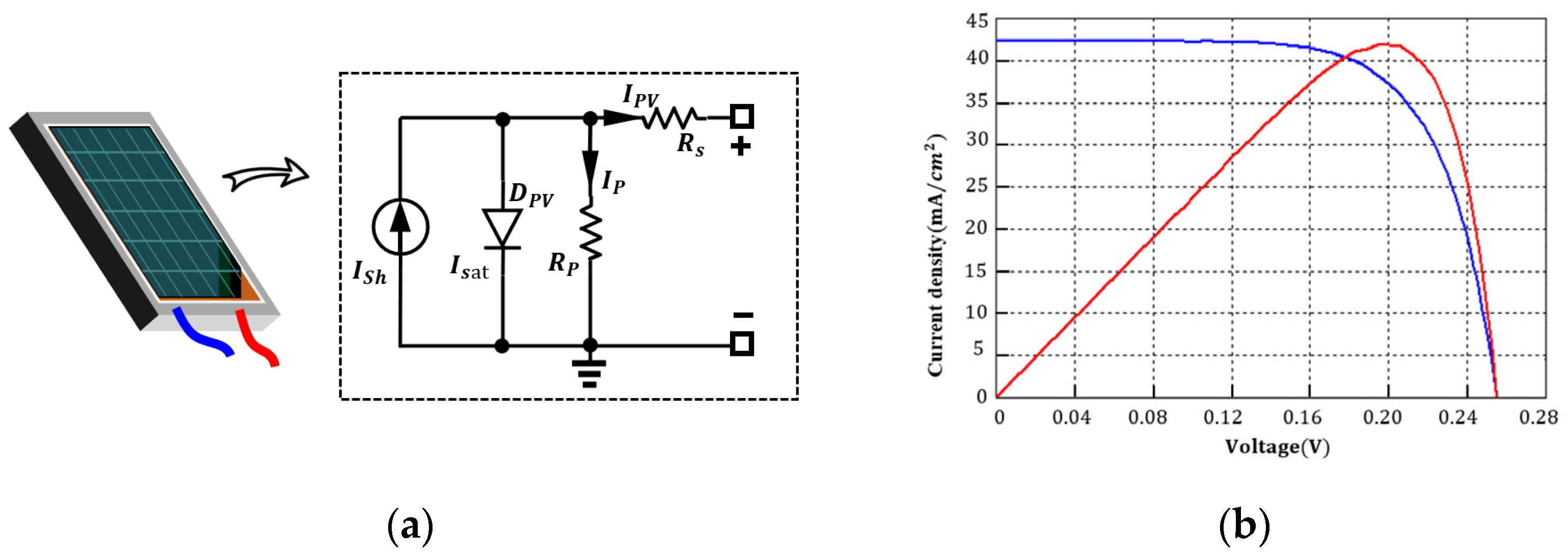
Figure 3a shows the equivalent circuit model of the PV module, and Figure 2b shows the volt-ampere characteristic curve of the PV module. According to the volt-ampere characteristics of Figure 3b, the small signal resistance rpv of the PV module can be obtained using the following Formula (1):
r p v = d v d i v p v ^ i p v ^
Through analysis, it is evident that when the PV module operates near the maximum power point, its small signal resistance assumes a negative value. At the same time, employing the state space averaging method to analyze the boost converter yields the state space equation of the system, represented by Formula (2):
d i L ^ d t d v p v ^ d t = R L L   1 C i n                 1 L 1 r p v C i n i L ^ v p v ^ + V D + V P V L 0
In Equation (2), VPV denotes the output voltage of the PV module, VD represents the forward conduction threshold voltage of the boost converter’s rectifier diode, RL stands for the parasitic resistance of the inductive device (which is typically small), and Cin signifies the input capacitance.
Solving the matrix Equation (2) yields the transfer function between the inductor current and the duty cycle of the control signal, which is expressed as Formula (3):
i L ^ d ^ = V D + V P V R L r p v 1 + s ω z a 2 s 2 + 2 a b s + a 2
a = r p v + R L r p v L C i n
b = r p v R L C i n L 2 a r p v L C i n
ω z = 1 r p v C i n
By analyzing Formula (3) and balancing the trade-off between loop speed and stability, MPPT loop control is achieved through the implementation of PI compensation.

2.3. Pulse Multiplication

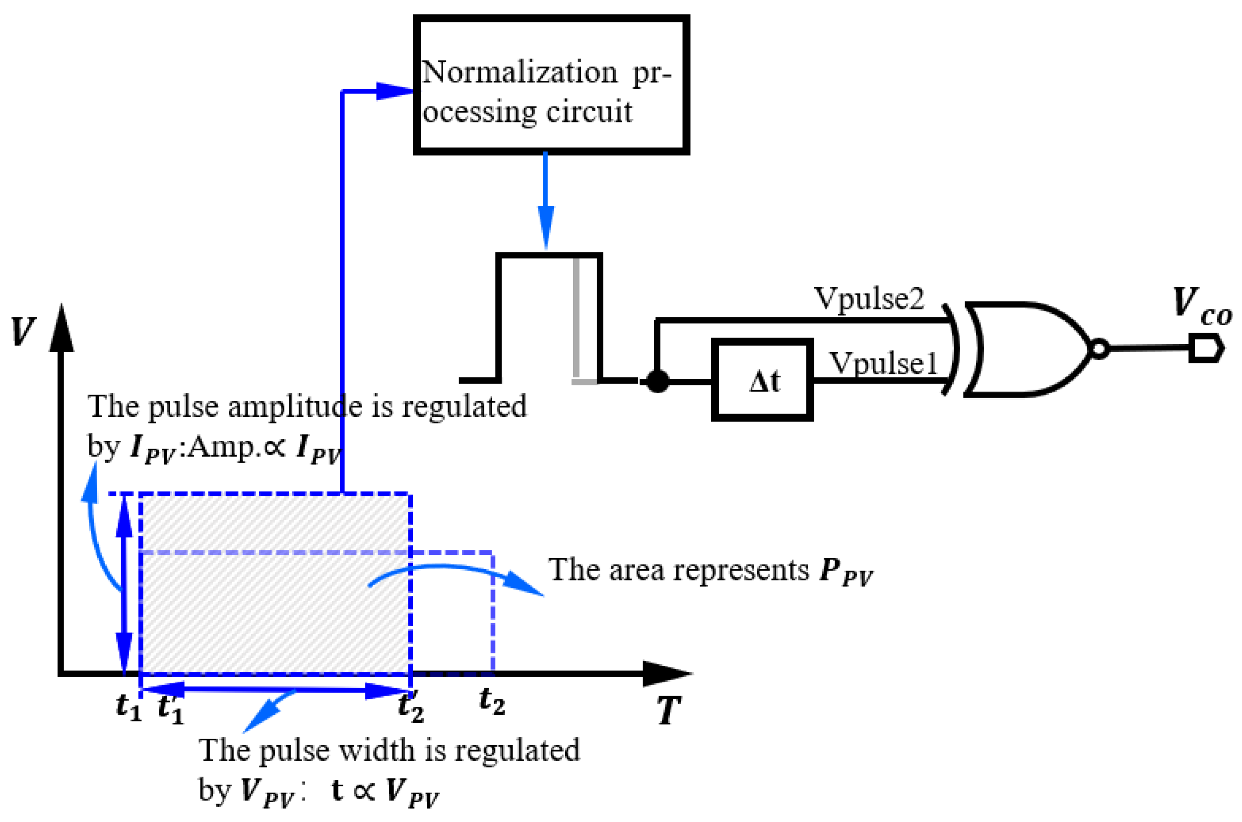
The novel pulse multiplication proposed in this paper is shown in Figure 4. This principle utilizes the output voltage of the PV module to regulate the width of a pulse signal while simultaneously using the output current of the PV to modulate the pulse signal’s amplitude. Consequently, the total area under the pulse signal curve directly corresponds to the output power of the PV module. Subsequently, the acquired pulse signal undergoes normalization, facilitating the representation of the PV module’s output power as pulse signals with uniform voltage amplitudes but varying widths. The normalized pulse signal is then processed through an XOR gate, with the output determining the direction of change in the PV module’s output power. This mechanism enables the implementation of the P&O MPPT with variable step size.
Figure 5 presents the structural block diagram of the MPPT. As the boost converter’s inductor is connected in series with the PV component, the output current of the PV corresponds to the current flowing through the inductor L. When the MPPT module is activated, the average current sampling circuit detects the output current of the PV module to regulate the pulse amplitude. Upon enabling the MPPT_EN signal, the pulse multiplier computes the output power of the PV component. Following computation, the results are forwarded to the XOR gate and SR flip-flop for power comparison. The comparison result is indicated by the VCO signal, where a value of 1 denotes increasing output power, while any other value indicates a decrease. Subsequently, the comparison result is transmitted to the voltage-tracking transmission rotation circuit to charge and discharge the CMPP capacitor, achieving variable step-size perturbation. For further insight into the circuit structure, refer to Section 3.2.

3. Circuit Implementation

The primary objective of this article is to enable energy harvesting from low-power miniature PV modules. However, it is important to note that the output power of PV modules diminishes as solar irradiance decreases. Even under optimal irradiance conditions, the output voltage of these miniature PV modules remains significantly below the threshold voltage required for MOSFET activation. Hence, the first step of low-voltage self-starting is designed in this article. It achieves low-voltage self-starting without relying on other forms of power sources.

3.1. Low-Voltage Cold Start-Up

Due to the insufficient voltage directly output by the PV source, the transistor fails to enter the strong inversion region and thus cannot conduct adequately. To address this issue, the output voltage of the PV must be elevated to surpass the threshold voltage of the transistor. Accordingly, a two-stage circuit comprising a voltage ring oscillator and a gate cross-coupled charge pump is employed to boost the initial voltage of the PV, as illustrated in Figure 6. The voltage gain of the gate cross-coupled charge pump is expressed by Equation (7):
V C = ( N + 1 ) V P V
where N represents the number of charge pump stages. Upon analyzing the power loss of the charge pump, it becomes evident that the primary losses encompass the switching and conduction losses of the MOS tube, along with the static power consumption of the charge pump. The switching loss and conduction loss are delineated by Formulas (8) and (9), respectively:
P S = C × f × V 2
P C = I L o a d 2 μ C o x W L ( V g s V t h )
where f represents the clock frequency of the charge pump drive, C denotes the pump capacitance of the charge pump, μ signifies the carrier mobility of the transistor, Cox denotes the gate oxide capacitance per unit area, and W/L represents the width-to-length ratio of the transistor. Equation (8) illustrates that the switching losses of the charge pump are directly proportional to the clock frequency that drives it. Moreover, the drive capability of the charge pump also correlates with the clock frequency, as depicted in Equation (10):
P = 4 × V 2 ( 1 + T R L o a d C + T 4 R L o a d C o u t ) 2 × R L o a d
where RLoad represents the on-resistance of the charge pump, T signifies the clock cycle that drives the charge pump, and Cout denotes the load capacitance of the charge pump. Equation (8) indicates that the switching losses of the charge pump are proportional to the clock driving it. Furthermore, Equation (10) demonstrates that the driving capability of the charge pump is also correlated with the clock frequency. Therefore, a novel low-voltage inverter is designed in this paper, as illustrated in Figure 7. During the charging phase, the input signal transitions from VDD to 0. Utilizing a PMOS transistor P3 with a reduced width-to-length ratio can further elevate the Y node voltage to VPV. This action significantly mitigates the VDS of the N2 transistor within the inverter structure, consequently lowering VGS and suppressing the leakage current Ioff. As a result, the output signal of the inverter achieves a high VH at a low power supply voltage. Conversely, during the discharge stage, when the input signal shifts from 0 to VDD, implementing an NMOS transistor N3 with a reduced aspect ratio facilitates further pulling down of the X-node voltage to GND. This action notably reduces |VDS| and |VGS| of the P2 transistor within the inverter structure, thereby suppressing the leakage current Ioff. Consequently, the inverter’s output signal attains a low VL at the supply voltage. Consequently, the new inverter exhibits faster turn-on and turn-off characteristics at low voltages and yields a higher output swing.
Compared with stacked low-voltage inverters, this structure is better suited for low-voltage ring oscillators used to generate clock signals for driving the charge pump. Furthermore, the gate cross-coupled charge pump necessitates a two-phase clock signal. However, overlapping of the two-phase clock signals driving the charge pump may induce a reverse leakage current. To mitigate dynamic losses of the charge pump and enhance its efficiency, the clock signal produced by the ring oscillator undergoes shaping, resulting in the generation of two-phase non-overlapping clock signals, labeled as ϕ and ϕ ¯ . Simultaneously, to optimize energy transfer post-system start-up, the low-voltage ring oscillator and charge pump circuit should be deactivated upon completion of start-up. Hence, to achieve this, a low-voltage inverter was substituted with a low-voltage NAND gate in the low-voltage ring oscillator, as depicted in Figure 8a. Ultimately, when the PV output voltage reaches 200 mV, the resulting clock frequency amounts to 124 kHz.
Figure 8b illustrates the structure of the voltage pulse trigger utilized in this study, with the voltage detection mechanism referenced from the literature [22]. As the ring oscillator initializes, the PV output voltage gradually rises. Upon detecting the charge pump output voltage reaching 500 mV, the voltage pulse trigger is activated, causing VPULSE to transition to a high level. This action turns on the auxiliary power transistor MA in Figure 6, thereby initiating PV charging of the inductor L. Concurrently, the EN signal of the ring oscillator transitions from 1 to 0, disabling the ring oscillator and causing the output voltage VC of the charge pump to gradually decline. Once VC drops below 500 mV, the EN signal shifts from 0 to 1, reactivating the ring oscillator. Subsequently, VPULSE transitions to 0, generating a pulse signal. During this step, MA is turned off, and the inductor current is discharged through the auxiliary starting circuit. To amplify the swing of the output voltage, an inverter is incorporated based on the voltage detector outlined in [22].

3.2. MPPT Circuit Based on Pulse Multiplication

In order to address the oscillation problem occurring near MPP with the traditional P&O MPPT method, a variable-step P&O MPPT circuit is designed in this paper. This circuit samples the output voltage and current of the PV source. Subsequently, the PV output power is calculated using pulse multiplication. Then, an XOR gate is employed to compare the current output power with that of the previous cycle, utilizing the high-level output time of the XOR gate to implement variable step perturbation for tracking MPP.
Figure 9 shows the structure of the MPPT circuit, which comprises a voltage-to-pulse signal circuit, an average current sampling circuit, and a voltage-to-time circuit. The green dashed box highlights the voltage-to-pulse signal section. The signal width of VP_CLK is directly proportional to that of VPV, denoted as
T p _ c l k = C 3 I 1 V P V V P V
When the MPPT_EN signal is activated, transitioning from 0 to 1, VP_CLK similarly transitions from 0 to 1. During this time, M4 is turned off, and M3 is turned on. Consequently, capacitor C3 begins charging through the bias current I1. As VC3 gradually rises, when it reaches VPV, VP_CLK transitions from 1 to 0, generating a pulse signal. While VP_CLK is at 1, the transmission is turned on, allowing the sampling current to charge capacitor C4. This process normalizes the pulse signal representing the output power of the PV module. The average current sampling circuit of the PV module is depicted in the blue dotted box. The orange dashed box depicts the circuit responsible for converting the voltage signal into a time domain signal. When VP_CLK is 1, capacitor C5 charges to VDD through M15, causing the output VP to be 0. At this point, the total charge stored in capacitors C4 and C5 is calculated as
Q = Q 4 + Q 5 = C 4 × V C 4 + C 5 × V C 5
When VP_CLK transitions to 0, and VP jumps to 1, the charges stored in the two nodes are discharged through M11 and M12. As the VC5 node reaches a low level through the discharge circuit, VP transitions back to 0. At this stage, the remaining charges on the two nodes are represented by Equation (13),
Q = Q 4 + Q 5 = C 4 × V C 4 + C 5 × V C 5
which determines the duration of the high voltage of the VP pulse signal. Pulse width TP can be expressed as
T p = ( C 4 × V C 4 + C 5 × V C 5 ) ( C 4 × V C 4 + C 5 × V C 5 ) I M 11
Figure 10 illustrates the MPPT turning circuit. Utilizing the VP signal generated in Figure 8, the VP signal obtained by sampling twice is output through an XOR gate to obtain VCO. When VP1 and VCO output high levels simultaneously, VC1 transitions from 0 to 1, and VCO’ transitions from 1 to 0, indicating a decrease in the output power of the PV module. Likewise, when VP2 and VCO output high levels simultaneously, VC2 outputs 1 and V CO’ outputs 1. This indicates an increase in the output power of the PV module. VCO’ is used to adjust the value of VMPP during tracking. The Qn of the D flip-flop represents the adjustment direction of VMPP in the current period, while Qn+1 represents the adjustment direction of the next period. If Qn+1 is 1, M19 is turned on to discharge through the current source controlled by VC1, reducing VMPP. Conversely, if Qn+1 is 0, M18 is turned on, and capacitor CMPP is charged through the current source controlled by VC2 to increase VMPP. The charging and discharging of CMPP are controlled by a voltage-controlled current source regulated by two signals. The charging time is determined by the difference in output power obtained by two samplings, enabling variable step size disturbance. This approach effectively mitigates oscillations near the MPP, thereby enhancing energy harvesting efficiency.

4. Results and Discussion

To validate the functionality of the proposed energy harvesting architecture, the system-on-chip was implemented using a 0.18 µm standard CMOS process and subjected to simulation and verification. The PV power source was substituted with an equivalent model comprising a current source, a diode, and two resistors. The PV module’s maximum open-circuit voltage was set to 250 mV, with a minimum output voltage of 80 mV and an output current range of 0.1–3 mA. To achieve a 1.2 V output from a 200 mV voltage source, the inductor L value of the boost converter was set to 1.5 mH. Considering the undershoot, overshoot, and ripple size of the output capacitor, a value of 12 pF was assigned to the output capacitor.
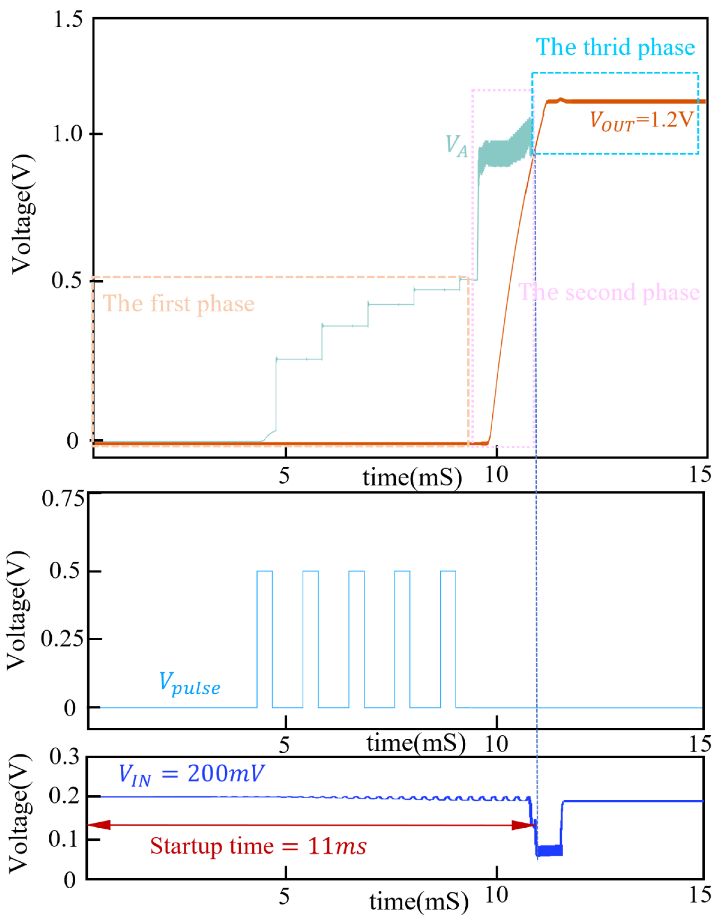
Figure 11 depicts the start-up sequence of the boost converter when the PV output voltage is 200 mV. In this scenario, MPPT activation occurs once the VOUT voltage reaches 1 V, indicating the completion of the cold start step. The cold start process spans 11 ms. The VPULSE signal governs the operation of the auxiliary power tube. Following five pulses, VA attains a voltage of 500 mV, transitioning into the second stage of the cold start step, thereby accelerating VA to 1 V. Upon VOUT reaching 1 V, the start-up process concludes, MPPT initiates, and the ultimate output voltage stabilizes at 1.2 V.
The tracking effect of the clock signal controlling the power tube MP and MPPT is depicted in Figure 12 when the output of the PV module changes. As the output voltage of the PV module gradually increases from 100 mV to 150 mV and the PV output voltage continuously transitions, the system can dynamically adjust the impedance of the energy collection system interface circuit to match the output impedance of the PV module, achieving MPPT. The input voltage Vin of the energy harvesting interface circuit is always equal to VPV/2.
Figure 13a illustrates the transient response of the output voltage when the load current abruptly transitions from 0 to 2.5 mA. Simulation outcomes demonstrate that despite a significant jump in the load current, the output voltage experiences only minor fluctuations, ensuring system stability. In Figure 13b, the MPPT process is depicted in response to load changes. While the load current remains constant, the system consistently operates at the maximum power point. Conversely, when the load varies, the system commences variable step-length tracking, swiftly converging to the maximum power point.
The conversion efficiency of the boost converter, as obtained through simulation, is depicted in Figure 14. Within the PV output voltage range of 90 mV to 300 mV, the converter achieves an overall efficiency exceeding 58%. Notably, at a PV output voltage of 220 mV, the peak efficiency of the boost converter reaches 93%. This remarkable efficiency is attributed to the variable-step P&O MPPT circuit proposed in this paper, which is based on the new pulse multiplication. This approach effectively resolves the trade-off between tracking speed and accuracy during maximum power point tracking. Moreover, the circuit’s simple structure contributes to lower energy consumption.
Table 1 shows the performance comparison with other previously developed PV energy harvesters. The proposed circuit achieves low-voltage self-starting while maintaining high energy transfer efficiency.

5. Conclusions

The self-starting technique with energy harvesting chips is interesting for research as it eliminates the need for additional external components. In this study, a three-step, low-voltage, self-starting boost converter has been developed with a remarkably low PV output voltage of 90 mV. By employing the variable-step P&O MPPT circuit based on the pulse multiplication, our system can accurately track the maximum power point. Additionally, the utilization of inductor average current for MPPT closed-loop control improves the stability during the tracking process. A peak efficiency of 93% is revealed in simulation tests when the PV output voltage reaches 220 mV. These features make it possible to perform energy harvesting at the milliwatt or even microwatt level for wearable IoT devices.

Author Contributions

Validation, writing—original draft preparation: N.W., S.X. and Z.H.; methodology, formal analysis: X.Z., Y.L. and Z.Z; writing—review and editing: S.X.; data curation and analysis: Y.L.; software, visualization: L.Z. and H.S.; investigation: Z.Z.; funding acquisition: Z.H.; project administration and resources: H.S. All authors have read and agreed to the published version of the manuscript.

Funding

This work is sponsored in part by the Shanghai Pujiang Programme under Grant 23PJD066, and in part by the Natural Science Foundation of Shanghai under Grant 21ZR1446300.

Data Availability Statement

Data are contained within the article.

Conflicts of Interest

Authors S.X., Y.L., Z.Z. and Z.H. were employed by the company 214 Institute of China North Industries. The remaining authors declare that the research was conducted in the absence of any commercial or financial relationships that could be construed as a potential conflict of interest.

References

  1. Zeb, H.; Gohar, M.; Ali, M.; Rahman, A.U.; Ahmad, W.; Ghani, A.; Choi, J.G.; Koh, S.J. Zero Energy IoT Devices in Smart Cities Using RF Energy Harvesting. Electronics 2023, 12, 148. [Google Scholar] [CrossRef]
  2. Statista. Available online: https://www.statista.com/statistics/471264/iot-number-of-connected-devices-worldwide/ (accessed on 17 December 2022).
  3. Nesbitt, R.; Shah, S.; Wagih, M.; Imran, M.; Abbasi, Q.; Ansari, S. Next-Generation IoT: Harnessing AI for Enhanced Localization and Energy Harvesting in Backscatter Communications. Electronics 2023, 12, 5020. [Google Scholar] [CrossRef]
  4. Nwalike, E.; Ibrahim, K.; Crawley, F.; Qin, Q.; Luk, P.; Luo, Z. Harnessing Energy for Wearables: A Review of Radio Frequency Energy Harvesting Technologies. Energies 2023, 16, 5711. [Google Scholar] [CrossRef]
  5. Shuvo, M.; Titirsha, T.; Amin, N.; Islam, S. Energy Harvesting in Implantable and Wearable Medical Devices for Enduring Precision Healthcare. Energies 2022, 15, 7495. [Google Scholar] [CrossRef]
  6. Abdellatif, S.; Moustafa, A.; Khalid, A.; Ghannam, R. Integration of Capacitive Pressure Sensor-on-Chip with Lead-Free Perovskite Solar Cells for Continuous Health Monitoring. Micromachines 2023, 14, 1676. [Google Scholar] [CrossRef] [PubMed]
  7. Kimiyoshi, U.; Songxiang, W.; Kaito, N.; Giovanna, L.; Paolo, M. A 200mV Operable On-Chip Temperature Sensor for IoT Devices Powered by Energy Harvesters with Ultra-Low Output Voltage. In Proceedings of the 2023 IEEE International Conference on Internet of Things and Intelligence Systems (IoTaIS), Bali, Indonesia, 28–30 November 2023. [Google Scholar] [CrossRef]
  8. Mahdi Elsiddig Haroun, F.; Mohamad Deros, S.N.; Ahmed Alkahtani, A.; Md Din, N. Towards Self-Powered WSN: The Design of Ultra-Low-Power Wireless Sensor Transmission Unit Based on Indoor Solar Energy Harvester. Electronics 2022, 11, 2077. [Google Scholar] [CrossRef]
  9. Ahmed, A.H.; Ahmed, N.M. An integrated thermal and RF energy harvesting system with rectifying combination and storage controller for IoT devices. Microelectron. J. 2023, 142, 106020. [Google Scholar] [CrossRef]
  10. Vullers, R.J.M.; van Schaijk, R.; Doms, I.; Van Hoof, C.; Mertens, R.M.E.H. Micropower energy harvesting. Solid-State Electron. 2009, 53, 684–693. [Google Scholar] [CrossRef]
  11. Ioannis, M.; Vasiliki, G.; Eftichios, K.; Stylianos, S. Integrated Maximum Power Point Tracking System for Photovoltaic Energy Harvesting Applications. IEEE Trans. Power Electron. 2022, 37, 9865–9875. [Google Scholar] [CrossRef]
  12. Jingcheng, T.; Wei, M.; Zhihong, L.; Lei, Z.; Chun-Huat, H. A Fully Integrated Power Converter for Thermoelectric Energy Harvesting with 81% Peak Efficiency and 6.4-mV Minimum Input Voltage. IEEE Trans. Power Electron. 2022, 37, 4968–4972. [Google Scholar] [CrossRef]
  13. Aatmesh, S.; Nathan, E.R.; Osama, U.K.; David, D.W.; Benton, H.C. A 10 mV-Input Boost Converter with Inductor Peak Current Control and Zero Detection for Thermoelectric and Solar Energy Harvesting with 220 mV Cold-Start and −14.5 dBm, 915 MHz RF Kick-Start. IEEE J. Solid-State Circuits 2015, 50, 1820–1832. [Google Scholar] [CrossRef]
  14. Rafael, L.R.; Mohamad, S.; Carlos, G.M.; Márcio, C.S. A 7.5-mV-Input Boost Converter for Thermal Energy Harvesting with 11-mV Self-Startup. IEEE Trans. Circuits Syst. II Express Briefs 2020, 67, 1379–1383. [Google Scholar] [CrossRef]
  15. Lianxi, L.; Yihe, X.; Wenbin, H.; Xufeng, L.; Yongyuan, L. A 10mV-500mV Input Range, 91.4% Peak Efficiency Adaptive Multi-Mode Boost Converter for Thermoelectric Energy Harvesting. IEEE Trans. Circuits Syst. I Regul. Pap. 2022, 69, 609–619. [Google Scholar] [CrossRef]
  16. Thinh, T.D.; Hieu, M.P.; Loan, P.N.; Sang-Gug, L.; Hanh-Phuc, L. Power Management IC with a Three-Phase Cold Self-Start for Thermoelectric Generators. IEEE Trans. Circuits Syst. I Regul. Pap. 2021, 68, 103–113. [Google Scholar] [CrossRef]
  17. Soumya, B.; Tejasvi, A.; Matthew, L.J. A 3.5-mV Input Single-Inductor Self-Starting Boost Converter with Loss-Aware MPPT for Efficient Autonomous Body-Heat Energy Harvesting. IEEE J. Solid-State Circuits 2021, 56, 1837–1848. [Google Scholar] [CrossRef] [PubMed]
  18. Tsung-Wei, H.; Hung-Hsien, W.; Dian-Lin, T.; Chia-Ling, W. Photovoltaic energy harvester with fractional open-circuit voltage based maximum power point tracking circuit. IEEE Trans. Circuits Syst. II Express Briefs 2019, 66, 257–261. [Google Scholar] [CrossRef]
  19. Hadeed, A.S.; Ali, F.M.; Abdullah, N.; Khaled, E.A.; Kamal, A.; Marcello, C. A New Sensorless Hybrid MPPT Algorithm Based on Fractional Short-Circuit Current Measurement and P&O MPPT. IEEE Trans. Sustain. Energy 2015, 6, 1426–1434. [Google Scholar] [CrossRef]
  20. Fangrui, L.; Shanxu, D.; Fei, L.; Bangyin, L.; Yong, K. A Variable Step Size INC MPPT Method for PV Systems. IEEE Trans. Ind. Electron. 2008, 55, 2622–2628. [Google Scholar] [CrossRef]
  21. Ahmed, M.; Harbi, I.; Kennel, R.; Abdelrahem, M. Predictive Fixed Switching Maximum Power Point Tracking Algorithm with Dual Adaptive Step-Size for PV Systems. Electronics 2021, 10, 3109. [Google Scholar] [CrossRef]
  22. Chen, P.H.; Ishida, K.; Ikeuchi, K.; Zhang, X.; Honda, K.; Okuma, Y.; Ryu, Y.; Takamiya, M.; Sakurai, T. Startup Techniques for 95 mV Step-Up Converter by Capacitor Pass-On Scheme and VTH-Tuned Oscillator with Fixed Charge Programming. IEEE J. Solid-State Circuits 2012, 47, 1252–1260. [Google Scholar] [CrossRef]
  23. HungHsien, W.; LiangYun, C.; ChiaLing, W. Wide-input-voltage-range and high-efficiency energy harvester with a 155-mV startup voltage for solar power. In Proceedings of the ESSCIRC 2017-43rd IEEE European Solid State Circuits Conference, Leuven, Belgium, 11–14 September 2017. [Google Scholar] [CrossRef]
  24. Daniel, S.T.; James, B.; Atul, W.; Alain, G.; David, D.W.; Benton, H.C. Modeling and Design of Cold-Start Charge Pumps for Photovoltaic Energy Harvesters. IEEE Trans. Circuits Syst. I Regul. Pap. 2023, 70, 4334–4345. [Google Scholar] [CrossRef]
  25. Zhiyuan, C.; Man-Kay, L.; Pui-In, M.; Rui, P.M. A Single-Chip Solar Energy Harvesting IC Using Integrated Photodiodes for Biomedical Implant Applications. IEEE Trans. Biomed. Circuits Syst. 2017, 11, 44–53. [Google Scholar] [CrossRef]
  26. Jinwei, Z.; Roghaieh, P.; Rami, G.; Man-Kay, L.; Finlay, W.; Muhammad, A.I.; Hadi, H. Self-Powered Implantable CMOS Photovoltaic Cell with 18.6% Efficiency. IEEE Trans. Electron Devices 2023, 70, 3149–3154. [Google Scholar] [CrossRef]
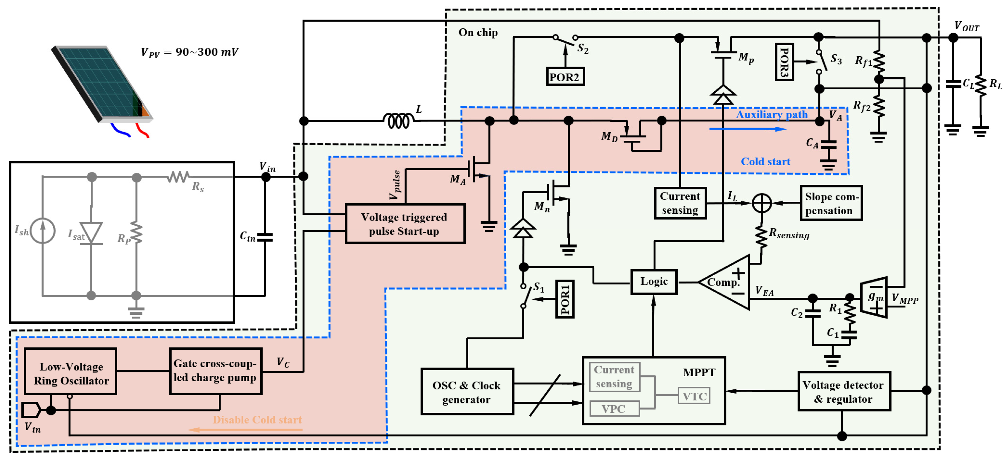
Figure 1. Low-voltage self-starting boost converter architecture (The cold start-up circuit is inside the blue dashed box; the circuit inside the black dashed box is on-chip).
Electronics 13 01713 g001
Figure 2. Illustrated three steps of operation: (a) boost converter start-up preprocessing; (b) boost converter auxiliary path enablement; (c) MPPT enablement (The cold start-up circuit within the blue dashed box is disabled).
Electronics 13 01713 g002
Figure 3. Illustrated PV characteristics. (a) PV equivalent circuit model; (b) Current-voltage (blue line) and power-voltage (red line) characteristics of PV.
Electronics 13 01713 g003
Figure 4. Novel pulse multiplication (The area within the blue dashed box represents the output power of the photovoltaic system).
Electronics 13 01713 g004
Figure 5. Structural block diagram of MPPT.
Electronics 13 01713 g005
Figure 6. Block diagram of the low-voltage start-up circuit for the first step.
Electronics 13 01713 g006
Figure 7. Low-voltage inverter (In the charging and discharging phases, only the black portion is enabled, while the gray portion is disabled).
Electronics 13 01713 g007
Figure 8. The first step is the critical circuit in the low-voltage cold start circuit. (a) Low-voltage ring oscillator (The detailed circuit structure within the blue dashed box is as indicated by the arrows); (b) voltage-triggered pulse circuit.
Electronics 13 01713 g008
Figure 9. Implementation of pulse multiplication.
Electronics 13 01713 g009
Figure 10. Direction decision and tracking circuit for MPPT (The circuit within the black dashed box represents the voltage-controlled voltage source; A–E represent the operating points of the PV during the MPPT process; the blue arrows indicate the variation of the PV operating points during the MPPT process).
Electronics 13 01713 g010
Figure 11. Transient response of boost converter at 200 mV.
Electronics 13 01713 g011
Figure 12. The MPPT tracking results and boost converter clock signal change when the PV output dynamically changes the transient response of the boost converter at 200 mV.
Electronics 13 01713 g012
Figure 13. Transient waveforms: (a) when ILoad changes from 0 to 2.5 mA; (b) when IPV changes from 3 to 0.2 mA.
Electronics 13 01713 g013
Figure 14. Estimated efficiency of the boost converter.
Electronics 13 01713 g014
Table 1. Performance comparison with other previous PV energy harvesters.
Reference[23][24][25][26]This Work
Start-up MethodRing oscillator + voltage multiplierRing oscillator + Auxiliary charge pumpNoRing oscillator + charge pump + auxiliary path
Technology (nm)1805518065180
MPPTNoYesNoNoYes
Self-Startup Voltage (mV)155365250No90
VPV (V)0.02–1.70.365–0.80.25–0.530.35–0.60.09–0.3
VIN,min (mV)20365250N/A90
VOUT (V)1.80.71.082.5 V1.2
Peak Efficiency[email protected] V48.9%0.436 V21.9%@0.31 V18.6%93%@0.22 V
Disclaimer/Publisher’s Note: The statements, opinions and data contained in all publications are solely those of the individual author(s) and contributor(s) and not of MDPI and/or the editor(s). MDPI and/or the editor(s) disclaim responsibility for any injury to people or property resulting from any ideas, methods, instructions or products referred to in the content.