Abstract
This paper presents a wideband low-power/low-voltage 60-GHz low-noise amplifier (LNA) in a 28-nm bulk CMOS technology. The LNA has been designed for high-speed millimeter-wave (mm-wave) communications. It consists of two pseudo-differential amplifying stages and a buffer stage included for 50-Ohm on-wafer measurements. Two integrated input/output baluns guarantee both simultaneous 50-ohm input–noise/output matching at input/output radio frequency (RF) pads. A power-efficient design strategy is adopted to make the LNA suitable for low-power applications, while minimizing the noise figure (NF). Thanks to the adopted design strategy, the post-layout simulation results show an excellent trade-off between power gain and 3-dB bandwidth (BW3dB) with 13.5 dB and 7 GHz centered at 60 GHz, respectively. The proposed LNA consumes only 11.6 mA from a 0.9-V supply voltage with an NF of 8.4 dB at 60 GHz, including the input transformer loss. The input 1 dB compression point (IP1dB) of −15 dBm at 60 GHz confirms the first-rate linearity of the proposed amplifier. Human body model (HBM) electrostatic discharge (ESD) protection is guaranteed up to 2 kV at the RF input/output pads thanks to the input/output integrated transformers.
1. Introduction
Wireless communications require increasing data rates that can be effectively achieved by exploiting the unlicensed industrial, scientific and medical (ISM) 60-GHz spectrum spanning from 57 GHz to 64 GHz [1]. However, the high atmospheric absorption in this frequency band limits the communication distance, thus enabling only short-range applications [2]. On the other hand, the wide 7-GHz bandwidth centered at 60 GHz guarantees wireless communications at Gbit/s data rates. As far as modulation is concerned, simple modulation schemes are preferred and, specifically, on–off keying (OOK) modulation is largely adopted in the literature since it is compatible with low-complexity circuits and low-power implementations [3,4,5,6,7]. Specifically, in the OOK architecture the receiver adopts non-coherent demodulation. As a result, the receiver does not require a local oscillator (LO), and the transmitter is not dependent on a phase-locked loop (PLL) to generate an exact frequency for the RF carrier [8].
Several interesting examples of 60-GHz OOK receivers have been published both in BiCMOS and CMOS technologies [9,10]. The most common receiver (RX) architecture adopts a wideband low-noise amplifier (LNA) that drives an OOK demodulator, typically consisting of an envelope detector (ED) and a baseband limiting amplifier (LA), as depicted in Figure 1. The main design target is minimizing the energy per bit required for demodulation at the minimum input signal power (i.e., sensitivity). Typical values of energy per bit are around 10 pJ/bit with the best values below 5 pJ/bit. As far as sensitivity is concerned, common levels are between −35 dBm and −25 dBm with a bit error rate (BER) of . Finally, power consumption is highly related to the data rate with typical values of about 20 mW at Gbit/s data rates.
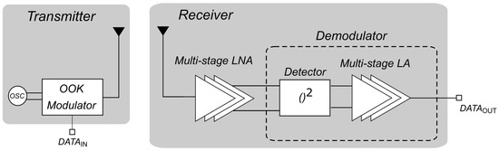
Figure 1.
Typical structure of an mm-wave OOK transceiver for high-speed applications.
The widespread design approach is mainly based on single-ended topologies for both the LNA and the demodulator to save power and silicon area and avoid single-ended-to-differential conversion at the millimeter-wave (mm-wave) input, while differential structures are more common in the baseband amplification stages. Multistage topologies (i.e., three, four and even five or six stages) are often proposed for the LNA to obtain a wideband gain at the expense of higher vulnerability to instability issues in a complete receiver [8,10]. Moreover, gm-enhancement techniques are also exploited to partially overcome the transconductance limitations of nanometer CMOS transistors at mm-wave frequencies, especially in bulk technologies. All the above-mentioned design approaches can hardly be adopted in an actual application that requires low power consumption, high rejection of common-mode noise interferences, and compatibility with implementation issues, such as electrostatic discharge (ESD) protection, especially at the mm-wave input/output.
To overcome the above limitations, a 60 GHz LNA for high-data-rate mm-wave receivers is proposed here. Its pseudo-differential topology along with an effective power-efficient design strategy allows for simultaneous input/noise matching with extremely low power consumption, making the amplifier suited for low-power mm-wave applications while providing intrinsic ESD protection. The proposed LNA includes two amplification stages and an output buffer stage. The simple two-stage topology is suited for a flat gain with a wide frequency bandwidth in the order of several gigahertz. On the other hand, adding a buffer stage provides 50-ohm output matching for single-ended on-wafer measurements and integrated ESD protection.
This paper is arranged as follows: Section 2 describes the architecture of the proposed LNA, and the adopted design approach is discussed in comparison with other state-of-the-art solutions. Section 3 introduces the adopted 28-nm CMOS technology and customized integrated passive components (i.e., integrated transformers and capacitors). The LNA layout and related post-layout simulation results are reported in Section 4, while the main conclusions are drawn in Section 5.
2. LNA Design
The LNA stage is crucial for the overall RF receiver. Indeed, it must guarantee impedance matching to the antenna and deliver a sufficiently high signal to the demodulator, while producing the lowest possible degradation of the signal-to-noise ratio (SNR) at the constrained power budget. Therefore, the amplifier topology is of utmost importance to optimize RX performance. Compared to more widely used multistage topologies, compact LNAs are more effective due to better linearity, that is, the input 1 dB compression point (IP1dB), and a reduced risk of oscillations in the entire receiver. However, achieving both sufficiently high gain and a wide frequency bandwidth becomes more challenging when the number of amplification stages is low. On the other hand, most mm-wave CMOS LNAs employ the single-ended architecture due to their lower power consumption, reduced silicon area and simplified architecture, particularly when avoiding the need for single-ended-to-differential conversion at the mm-wave input. These factors make single-ended topologies attractive in scenarios where a minimal power budget and compact layout are the main constraints. However, single-ended structures are inherently more susceptible to common-mode noise injected from the supply voltage and/or substrate, especially at mm-wave frequencies, and offer no intrinsic path for ESD protection. Based on these considerations, the LNA depicted in Figure 2 has been designed.
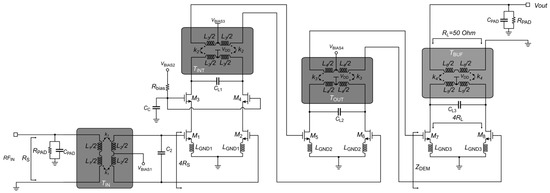
Figure 2.
Simplified schematic of the proposed stand-alone 60-GHz LNA.
The differential input of the amplifier is connected to a 50-ohm single-ended antenna by means of the integrated input transformer, TIN, which also provides impedance matching and ESD protection. The LNA adopts a pseudo-differential structure and consists of two amplification stages and an output buffer. Integrated transformers TINT/TOUT are extensively exploited as resonant loads, while enabling simple interstage connections and biasing. Despite the low supply voltage, VDD, of 0.9 V, for the input stage of the LNA, the cascode (CAS) topology has been preferred to a more widely used common-source (CS) one. Indeed, the CS-based configuration exhibits better noise performance, but suffers from extremely poor input/output isolation, which involves the design of input/output matching networks, and can also lead to instability. On the other hand, both second and buffer stages adopt the CS topology to exploit all the available voltage headroom and maximize LNA linearity. It is worth noting that inductive degeneration (i.e., LGND1, LGND2 and LGND3) models the parasitic path toward ground.
As proposed in [11], power-efficient simultaneous noise impedance matching with source impedance transformation (PE-SNIM) is used for the first stage, given that conventional design methods for noise/impedance matching do not consider the constraints of the current budget in mm-wave CMOS LNAs. PE-SNIM guarantees simultaneous noise and impedance matching at a low current level by means of inductive degeneration, LGND1, and proper sizing of the W/L ratio of the M1,2 pair. Specifically, an integrated transformer performs input impedance transformation, thus allowing each LNA branch to be matched to 2RS instead of RS/2 by means of inductive degeneration, LGND1 (i.e., the parasitic path toward the ground plane). With a transistor bias current of only 2.6 mA, the first stage of the LNA achieves simultaneous noise/input matching thanks to the 1:4 input impedance step-up (i.e., from 50 Ω to 200 Ω) provided by the integrated transformer, TIN. It is worth noting that the adoption of a traditional 1:1 input impedance ratio would require a differential stage with a current consumption about four times higher. As a result, the overall current required by the first differential stage (i.e., 5.2 mA) is almost the same as a single-ended amplifier, while guaranteeing superior robustness against common-mode noise/disturbances and ESD protection.
The second stage is essential to extend the 3-dB bandwidth (BW3dB) of the amplifier in order to comply with multi Gbit/s applications. The first stage is connected to the second one by means of the integrated interstage transformer, TINT, which not only provides the interstage matching, but also biases the following stage through its center tap without requiring coupling capacitors. Indeed, series coupling capacitors are not effective due to their excessive losses at mm-wave frequencies. Flat gain and a large BW3dB are achieved by properly tuning the load capacitors, CL1 and CL2, which are in parallel with the two integrated transformers, TINT and TOUT, respectively. As the last stage, the buffer also exploits a CS pseudo-differential topology with a transformer load, TBUF. The transformer has been designed to provide wideband 50-ohm output matching and differential-to-single-ended conversion resonating with capacitor CL3. Moreover, the buffer provides high input impedance as the second-stage output load (i.e., ZDEM) to preserve the voltage gain of the two-stage amplifier, as happens when the LNA is connected to a demodulator. It is worth noting that buffer functionalities cannot be achieved by means of an output passive matching network. By choosing proper resonance frequencies of the three integrated transformers TINT, TOUT and TBUF, a BW3dB of nearly 7 GHz can be guaranteed.
3. Integration Technology and Passive Component Design
The proposed LNA has been designed in a TSMC 28-nm bulk CMOS technology that features a 9-metal back-end-of-line (BEOL) with a top 3.5-µm ultrathick metal (M9) plus a thick alucap layer (AP) of 2.8 µm. The process provides low-voltage-threshold (LVT) 0.9-V CMOS transistors that are suited for low-power/high-frequency operation. Moreover, the design kit (DK) also includes accurate models of CMOS transistors based on measurements up to 110 GHz with metal connections up to metal 3. Unfortunately, no inductive components are available, while standard metal–oxide–metal (MOM) interdigitated capacitors have a very poor quality factor (Q-factor) at mm-wave frequencies. The lack of passive components suited for low-loss LC resonant networks is a big challenge and requires the customized design of both integrated transformers and capacitors.
Passive Component Design
Integrated transformers are crucial for the design of the proposed LNA. Generally, stacked windings provide the highest magnetic coupling factor, k, and optimal area efficiency. Interleaved or tapped structures suffer from larger footprints and lower k, while interstacked transformers can be effectively implemented if two equal metal layers are available. The choice of the most suitable transformer topology among tapped, interleaved, stacked and interstacked ones depends on the BEOL (i.e., thickness of the metals, intermetal oxide thickness, distance from the substrate, etc.) and circuit specifications. Although ground shields are often included beneath the coils to reduce the substrate losses, their effectiveness is quite poor at mm-wave frequencies and they reduce the self-resonance frequency (SRF). For these reasons, no ground shields were adopted [12]. The very first design step was the definition of the transformer topology and winding geometries by means of paper-and-pencil calculations in order to meet circuit specs. Then, transformer optimization was carried out by means of electromagnetic (EM) simulations to maximize the magnetic coupling factor, k, and the Q-factor at 60 GHz, while trading off the SRF.
As already explained, the input transformer, TIN, is responsible for simultaneous noise/input matching based on the impedance transformation PE-SNIM technique, along with ESD protection. Specifically, a turn ratio, N, of about 2 is required to perform impedance transformation from RS to 4RS (i.e., 50 Ω to 200 Ω). This means that the secondary coil inductance, L2, should be about four times higher than the primary one L1. Figure 3 depicts the transformer structure used to implement TIN. It exploits an octagonal shape and the topmost and thickest metal layers, AP and M9 for L1 and L2, respectively, in order to reduce the resistive losses and minimize the capacitive parasitics of the coils toward the substrate, therefore maximizing both the Q-factor and SRF. The stacked configuration is adopted to take advantage of the high magnetic coupling factor, k, by choosing different metal widths, w, for primary and secondary spirals, as depicted in Figure 3a,b. Indeed, this configuration allows us to use one-turn and two-turn coils for primary and secondary windings, respectively, and thus to implement the turn ratio required for input impedance transformation while preserving the stacked configuration, as shown in Figure 3c. Specifically, the primary coil adopts an alucap width of 8 µm that helps to improve the Q-factor without affecting the SRF. A lower width of 3 µm is instead used for the secondary coil that is built in metal 9. As far as ESD protection is concerned, the adopted 28-nm CMOS technology defines a minimum AP width of 1.44 µm tolerating an ESD current of 1.3 A for the 2-kV human body model (HBM), which fully complies with the width of the primary coil of TIN. Moreover, the LNA input is connected to a standard model for the HBM test consisting of a series resistor and a capacitor with the values of 1.5 kΩ (average skin resistance) and 100 pF (average body capacitance), respectively [3,4]. A 2-kV ESD protection is achieved, guaranteeing that the gate voltages of the input pair, M1,2, are well below the breakdown voltage of 1 V.
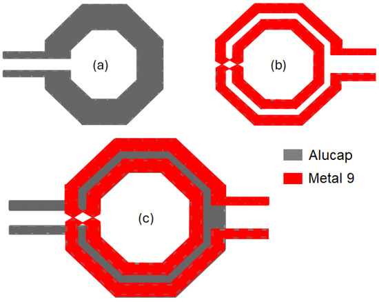
Figure 3.
Transformer, TIN: primary coil, L1 (a); secondary coil, L2 (b); stacked transformer (c).
Based on 2D EM simulations with ADS MomentumTM, the primary, L1, and secondary, L2, inductance values of transformer TIN are 47 pH and 143 pH at 60 GHz, respectively, while the magnetic coupling factor, k, is 0.59. It is well known that minimizing the input matching network loss requires equal resonance frequencies for both primary and secondary windings. In this case, regardless of the value of k, the impedance is transferred by the square of the turn ratio, N2 = L2/L1, which is about 3 for the adopted TIN. Therefore, to achieve the required impedance transformation, the primary-winding resonance frequency is set a little bit higher than the secondary one. Indeed, in this case, at the expense of slightly higher loss in the network, the impedance is theoretically transferred by the factor of [13]. The latter should be higher than 4 to compensate for non-idealities of the transformer and guarantee 1:4 impedance transformation. The first tuning of the input matching network is performed, while fine-tuning is carried out by using final post-layout EM simulations.
Both interstage and output transformers, TINT and TOUT, adopt a one-turn octagonal stacked topology by using M9 and AP layers for the primary and secondary spirals, respectively. The stacked configuration guarantees the highest values of the transformer characteristic resistance (TCR) thanks to a magnetic coupling factor as high as k values of 0.7, thus enabling better gain values for both stages. It is worth mentioning that due to the different thicknesses of AP and M9, there is a small difference in terms of the inductance and Q-factor between the primary and the secondary coils. For this reason, the primary coils, L3 and L5, of TINT and TOUT, respectively, are implemented on M9.
Finally, the 50-ohm output matching and differential-to-single-ended conversion are achieved by means of the integrated transformer, TBUF. The latter adopts the same geometry of the input transformer TIN. A summary of geometrical and EM-extracted parameters of the three integrated transformers is reported in Table 1.

Table 1.
Geometrical/electrical parameters of integrated transformers of the LNA.
The performance of the LNA is highly affected by the losses of the LC resonant networks formed by the above-described integrated transformers and capacitors (i.e., C2, CL2, CL2 and CL3). In the adopted 28-nm CMOS technology, available standard MOM capacitors have very poor Q-factors at 60 GHz (i.e., about 15) along with very high process variations that impact both gain and frequency bandwidth performance. For this reason, customized differential metal–insulator–metal (MIM) capacitors have been designed to be used instead of MOM capacitors. These MIM capacitors are implemented by means of two top metal layers of AP and M9, as shown in Figure 4. Though not standard, MIM capacitors have been designed to be fully compatible with the TSMC 28-nm process, minimizing reliability risks. The EM-simulated Q-factor is as high as 100 at 60 GHz, which guarantees reduced losses of the resonant LC networks of the LNA.
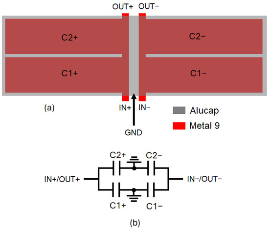
Figure 4.
Differential MIM capacitor: layout (a) and equivalent circuit (b).
4. Layout Description and Expected Performance
4.1. Layout and EM Post-Layout Analysis
Figure 5 depicts the layout of the 60-GHz LNA core, whose size is 445 µm × 140 µm (excluding PADs for measurement setup), main labels for the LC resonant networks (i.e., transformers and MIM capacitors) and the ground (GND) plane, also included for the sake of clarity. The chip has been drawn for on-wafer measurements through GSG RF probes at both input and output (east/west positions) by using a two-port network analyzer. Multi-contact DC probes (north/south positions, not displayed in Figure 5) are instead adopted for DC biasing. As already detailed in the previous sections, on-chip ESD protection is provided at both RF input and output by means of transformers, TIN and TBUF. A metal GND plane was implemented by using the top alucap layer, while complying with the metal density rules of the adopted technology. At mm-wave frequencies, the layout parasitics highly affect circuit performance, and therefore, careful estimation is of utmost importance. In this design, the overall LNA layout, including integrated transformers (TIN, TINT, TOUT and TBUF), customized MIM capacitors (C2, CL1, CL2 and CL3), transistor connections, DC paths and the metal ground plane, has been EM-simulated with ADS MomentumTM by using the substrate layer description provided by TSMC.
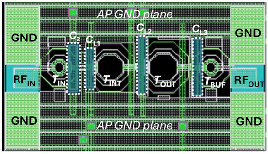
Figure 5.
Layout of the proposed LNA.
It is worth noting that despite the high computational complexity of such EM simulation, this is mandatory to properly estimate all the couplings taking place in the LNA, thereby helping to identify and eliminate potential sources of instability. However, a full EM simulation of the complete LNA layout was performed only at the final stage of the design process. Prior to this, iterative EM simulations of individual LNA sections—particularly the LC resonant networks—were conducted to guide the design according to the simplified procedure illustrated in Figure 6.
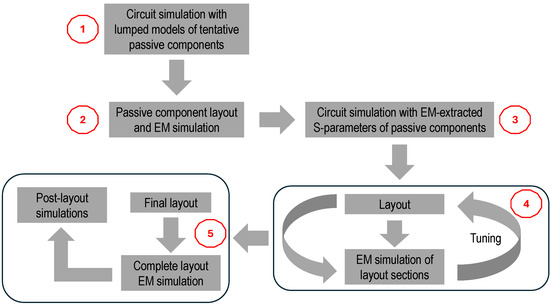
Figure 6.
Simplified design procedure adopted for the 60-GHz LNA.
4.2. Expected Performance
Figure 7, Figure 8 and Figure 9 illustrate the LNA performance at nominal supply voltage and room temperature. The overall LNA current consumption at a 0.9-V supply voltage is as low as 11.6 mA, including 3.2 mA for the output buffer. The input (S11) and output (S22) scattering parameters (S-parameters) are shown in Figure 7. They confirm the soundness of the adopted input/output transformer-based networks, which guarantee wideband matching centered at 60 GHz. Figure 8 depicts the voltage gain of the two-stage LNA, which is as high as 20 dB with a BW3dB of more than 7 GHz, and compares it with the LNA power gain, S21 (i.e., 50 Ω input/output matching), including the output buffer. The amplifier achieves a power gain of 13.5 dB, while preserving a 7-GHz BW3dB centered at 60 GHz.
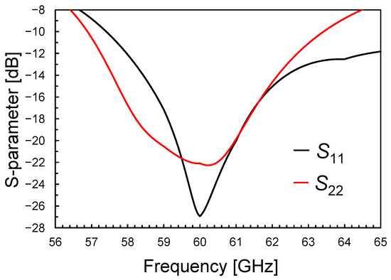
Figure 7.
Input (S11) and output (S22) matching versus frequency.
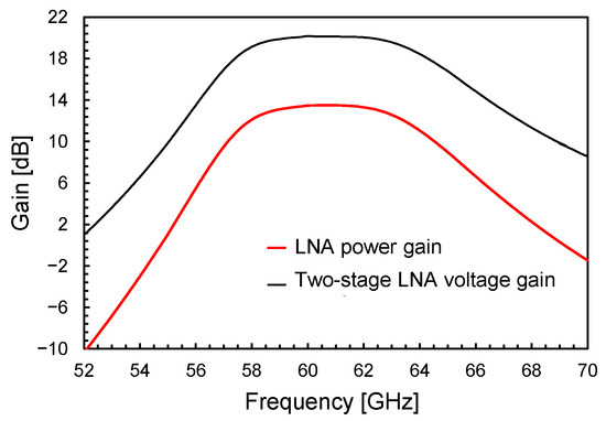
Figure 8.
Two-stage LNA voltage gain and power gain, S21, of the two-stage LNA with the buffer.
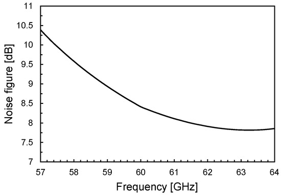
Figure 9.
Noise figure, NF, versus frequency.
The noise figure of the LNA is shown in Figure 9 and is primarily determined by the first two amplification stages. It reaches approximately 8.4 dB at 60 GHz and remains below 10.5 dB across the entire ISM frequency band. Notably, this performance is achieved with very low power consumption—approximately 10.4 mW—enabled by the PE-SNIM technique. It is worth mentioning that in an actual 60-GHz OOK receiver, such NF performance enables a sensitivity of about −40 dBm, which is better than typical sensitivity values reported in the state of the art. The linearity of the LNA is assessed using the input 1-dB compression point (IP1dB), as illustrated in Figure 10. The LNA demonstrates an IP1dB of around −15 dBm, which exceeds the maximum input levels encountered in typical application scenarios (i.e., about −25 dBm). The stability of the LNA, including layout parasitics, has been verified by using Rollett’s stability factor. Simulations in nominal and worst-case conditions indicate that the amplifier is unconditionally stable.
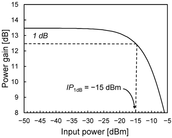
Figure 10.
LNA power gain versus input power.
For the sake of completeness, the sensitivity of the proposed LNA is verified by means of Montecarlo (MC) simulations. Figure 11 summarizes the MC results for the main LNA performance parameters, i.e., power gain, NF, S11 and S22 at 60 GHz, BW3dB and IP1dB.
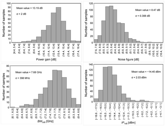
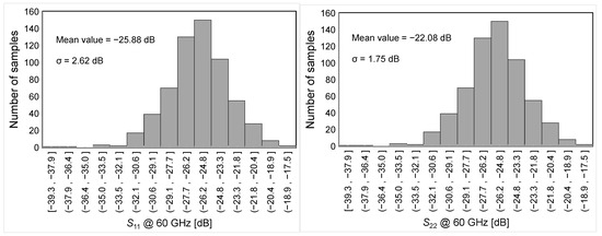
Figure 11.
MC-simulated results for main LNA performance parameters.
A comparison of the proposed 60-GHz LNA with the recent state of the art is summarized in Table 2. The LNA shows an excellent trade-off between the main design parameters, which are evaluated through several figures of merit (FoMs) introduced in [14,15,16,17,18]. The proposed FoMs consider the most critical LNA design parameters including gain, frequency bandwidth, noise, linearity and DC power consumption (PDC). Thanks to the PE-SNIM technique, despite having ESD protection and a differential structure, the proposed LNA consumes considerably lower power, PDC, with respect to recent state-of-the-art works. Moreover, ESD protection, which is guaranteed through input/output transformers at the expense of a higher NF, is often neglected in most of the 60-GHz LNA designs., Although the LNA in [19] guarantees HBM ESD protection up to 3 kV ESD, it consumes at least three times more power than the proposed LNA, given that ESD protection is more challenging in nanoscale technologies.
Table 2.
LNA performance and comparison with the state of the art.
5. Conclusions: Main Achievements, Pioneering Research and Future Directions
This paper presented the design of a wideband, low-power/voltage 60 GHz LNA in 28 nm bulk CMOS technology, specifically tailored for high-speed mm-wave wireless communication systems. The proposed LNA includes a pseudo-differential two-stage amplifier followed by an output buffer stage, optimized using the PE-SNIM strategy. This technique enables differential operation with ultra-low power consumption, traditionally a challenge in nanoscale CMOS, while maintaining impedance/noise matching. A key innovation of this work is the integration of customized LC resonant networks, made up of stacked coils and differential MIM capacitive structures, which were properly co-designed to obtain compact low-loss on-chip matching, ensuring broadband gain performance. Furthermore, input/output transformers also serve as an intrinsic path for ESD protection, achieving up to 2-kV HBM robustness, an often overlooked yet essential feature in mm-wave designs.
Post-layout EM simulations confirm the effectiveness of the proposed design, showing a power gain of 13.5 dB, a 7-GHz BW3dB centered at 60 GHz, an NF of 8.4 dB and an IP1dB of −15 dBm, with a total power consumption of just 10.4 mW from a 0.9-V supply voltage. The LNA meets the stringent requirements of high-speed, low-power OOK-based mm-wave receivers and compares favorably with recent state-of-the-art solutions. This work is among the few in the literature to demonstrate a differential, ESD-protected 60 GHz CMOS LNA that combines low power, low voltage and wide bandwidth, all within a compact and integration-friendly layout. The use of the PE-SNIM technique within a pseudo-differential structure under such strict power constraints represents a significant advancement for energy-efficient mm-wave front-end circuits.
However, some limitations and challenges must be acknowledged. The performance figures are based on post-layout simulations, and further silicon validation is essential to confirm the results under real measurement conditions. Moreover, while the custom-designed transformers and MIM capacitors offer excellent performance, their implementation requires tight control over layout density rules, parasitic modeling and process variation, which can introduce yield or integration issues when porting to other foundries or scaling to system-on-chip (SoC) platforms. These factors may also affect matching, gain flatness or ESD tolerance if not carefully managed.
Looking ahead, several research directions are envisioned:
- Integration with OOK demodulator to evaluate complete receiver performance in terms of sensitivity and energy per bit.
- Exploration of reconfigurable bandwidth or gain control via tunable passive elements for adaptive communication environments.
- Investigation into co-design strategies for ESD and matching, to reduce area and further improve robustness without degrading performance.
- Scalability to higher frequencies by redesigning transformers and layout techniques while managing increased losses and EM coupling.
In conclusion, the proposed LNA represents a promising and practical solution for next-generation mm-wave wireless systems, offering a compelling combination of performance, power efficiency and integration readiness.
Author Contributions
Conceptualization, M.E. and E.R.; validation, M.E., A.B. and E.R.; formal analysis, M.E. and E.R.; methodology, M.E. and E.R.; project administration, E.R., G.G. and S.P.; supervision, E.R., G.G. and A.B.; writing—original draft, M.E. and E.R.; writing—review and editing, M.E., G.G., A.B., S.P. and E.R. All authors have read and agreed to the published version of the manuscript.
Funding
This work was partially supported by the European Union under the Italian National Recovery and Resilience Plan (PNRR) of Next Generation EU, partnership on “Telecommunications of the Future” (PE0000001—program “RESTART”).
Data Availability Statement
The data presented in this study is available on request from the corresponding author.
Conflicts of Interest
The authors declare no conflicts of interest.
References
- Rappaport, T.S.; Murdock, J.N.; Gutierrez, F. State of the art in 60-GHz integrated circuits and systems for wireless communications. Proc. IEEE 2011, 99, 1390–1436. [Google Scholar] [CrossRef]
- Ferschischi, A.; Rehman, S.U.; Rieß, V.; Carta, C.; Ellinger, F. 20 Gb/s 60-GHz OOK receiver for high-data-rate short-range wireless communications. In Proceedings of the 2020 15th European Microwave Integrated Circuits Conference (EuMIC), Utrecht, The Netherlands, 10–15 January 2021; pp. 45–48. [Google Scholar]
- Byeon, C.W.; Yoon, C.H.; Park, C.S. A 67-mW 10.7-Gb/s 60-GHz OOK CMOS transceiver for short-range wireless communications. IEEE Trans. Microw. Theory Tech. 2013, 61, 3391–3401. [Google Scholar] [CrossRef]
- Ferchischi, A.; Rehman, S.U.; Carta, C.; Ellinger, F. 22-Gb/s 60-GHz OOK demodulator in 0.13-µm SiGe BiCMOS for ultra-high-speed wireless communication. In Proceedings of the IEEE MTT-S International Microwave Symposium (IMS), Boston, MA, USA, 2–7 June 2019; pp. 247–250. [Google Scholar]
- Zhu, F.; Hong, W.; Liang, W.-F.; Chen, J.; Jiang, X.; Yan, P.; Wu, K. A low-power low-cost 45-ghz ook transceiver system in 90-nm CMOS for multi-Gb/s transmission. IEEE Trans. Microw. Theory Tech. 2014, 62, 2105–2117. [Google Scholar] [CrossRef]
- Lin, F.; Brinkhoff, J.; Kang, K.; Pham, D.D.; Yuan, X. A low power 60GHz OOK transceiver system in 90 nm CMOS with innovative onchip AMC antenna. In Proceedings of the IEEE Asian Solid-State Circuits Conference, Taipei, Taiwan, 6–18 November 2009; pp. 349–352. [Google Scholar]
- Lee, J.J.; Byeon, C.W.; Eun, K.C.; Oh, I.Y.; Park, C.S. Gbps 60 GHz CMOS OOK modulator and demodulator. In Proceedings of the IEEE Compound Semiconductor Integrated Circuit Symposium (CSICS), Monterey, CA, USA, 3–6 October 2010; pp. 145–149. [Google Scholar]
- Byeon, C.W.; Eun, K.C.; Park, C.S. A 2.65-pJ/Bit 12.5-Gb/s 60-GHz OOK CMOS transmitter and receiver for proximity communications. IEEE Trans. Microw. Theory Tech. 2020, 68, 2902–2910. [Google Scholar]
- Byeon, C.W.; Lee, J.J.; Eun, K.C.; Park, C.S. A 60 GHz 5 Gb/s Gain-Boosting OOK demodulator in 0.13 μm CMOS. IEEE Microw. Wirel. Compon. Lett. 2011, 21, 101–103. [Google Scholar] [CrossRef]
- Uzunkol, M.; Shin, W.; Rebeiz, G.M. Design and analysis of a low-power 3–6-Gb/s 55-GHz OOK receiver with high-temperature performance. IEEE Trans. Microw. Theory Tech. 2012, 60, 3263–3271. [Google Scholar] [CrossRef]
- Eghtesadi, M.; Giustolisi, G.; Ballo, A.; Pennisi, S.; Ragonese, E. A 5 mW 28 nm CMOS low-noise amplifier with transformer-based electrostatic discharge protection for 60 GHz applications. Electronics 2024, 13, 4285. [Google Scholar] [CrossRef]
- Spataro, S.; Salerno, N.; Papotto, G.; Ragonese, E. The effect of a metal PGS on the Q-Factor of spiral inductors for RF and mm-wave applications in a 28-nm CMOS technology. Int. J. RF Microw. Comput. Aided Eng. 2020, 30, e22368. [Google Scholar] [CrossRef]
- Bevilacqua, A. fundamentals of integrated transformers: From principles to applications. IEEE Solid-State Circuits Mag. 2020, 12, 86–100. [Google Scholar] [CrossRef]
- Huang, C.C.; Kuo, H.C.; Huang, T.H.; Chuang, H.R. Low-power, high-gain V-band CMOS low noise amplifier for microwave radiometer applications. IEEE Microw. Wirel. Compon. Lett. 2011, 21, 104–106. [Google Scholar] [CrossRef]
- Gramegna, G.; Paparo, P.; Erratico, P.G.; De Vita, P. A sub-1dB NF ±2.3kV ESD-protected 900-MHz CMOS LNAs. IEEE J. Solid-State Circuits 2001, 36, 1010–1017. [Google Scholar] [CrossRef]
- Hsu, M.-T.; Lin, Y.-H.; Yang, J.-C. Design of UWB CMOS LNA based on current-reused topology and forward body-bias for high figure of merit. In Proceedings of the 2013 Asia-Pacific Microwave Conference (APMC), Seoul, Republic of Korea, 5–8 November 2013; pp. 772–774. [Google Scholar]
- Asgaran, S.; Deen, M.J.; Chen, C. -H. Design of the input matching network of RF CMOS LNAs for low-power operation. IEEE Trans. Circuits Syst. I Regul. Pap. 2007, 54, 544–554. [Google Scholar] [CrossRef]
- Fritsche, D.; Tretter, G.; Carta, C.; Ellinger, F. Millimeter-wave low-noise amplifier design in 28-nm low-power digital CMOS. IEEE Trans. Microw. Theory Tech. 2015, 63, 1910–1922. [Google Scholar] [CrossRef]
- Lin, C.Y.; Chu, L.W.; Ker, M.D. ESD protection design for 60-GHz LNA with inductor-triggered SCR in 65-nm CMOS process. IEEE Trans. Microw. Theory Tech. 2012, 60, 714–723. [Google Scholar] [CrossRef][Green Version]
- Han, A.; Luo, X. A 60-GHz current-reused cascode noise-canceling low noise amplifier. IEEE Trans. Circuits Syst. II Express Briefs 2024, 71, 4809–4813. [Google Scholar] [CrossRef]
- Bierbuesse, D.; Negra, R. 60 GHz variable gain & linearity enhancement LNA in 65 nm CMOS. In Proceedings of the IEEE Radio Frequency Integrated Circuits Symposium, Los Angeles, CA, USA, 4–6 August 2020; pp. 163–166. [Google Scholar]
- Cheng, D.; Chen, X.; Chen, Q.; Li, L. Design of an ultra-compact 60-GHz bi-directional amplifier in 65-nm CMOS. IEEE Microw. Wirel. Compon. Lett. 2022, 32, 343–346. [Google Scholar] [CrossRef]
- Ke, J.; Feng, G.; Wang, Y. A compact 60 GHz LNA with 22.7-dB gain and 4.4-dB NF in 40 nm CMOS. In Proceedings of the IEEE International Conference on Integrated Circuits, Technologies and Applications, Xi’an, China, 28–30 October 2022; pp. 152–153. [Google Scholar]
- Nawaz, A.A.; Albrecht, J.D.; Ulusoy, A.C. A 28-/60-GHz band switchable bidirectional amplifier for reconfigurable mm-wave transceivers. IEEE Trans. Microw. Theory Tech. 2020, 68, 3197–3205. [Google Scholar] [CrossRef]


Disclaimer/Publisher’s Note: The statements, opinions and data contained in all publications are solely those of the individual author(s) and contributor(s) and not of MDPI and/or the editor(s). MDPI and/or the editor(s) disclaim responsibility for any injury to people or property resulting from any ideas, methods, instructions or products referred to in the content. |
© 2025 by the authors. Licensee MDPI, Basel, Switzerland. This article is an open access article distributed under the terms and conditions of the Creative Commons Attribution (CC BY) license (https://creativecommons.org/licenses/by/4.0/).