Abstract
The design of transformers, a key component of radio frequency integrated circuits (RFICs), is traditionally carried out through an iterative process involving extensive electromagnetic simulations. While process design kits (PDKs) offer tools based on interpolation or fitting equations to simplify parameter estimation, these tools are restricted to standard geometries, leaving designers to manually simulate and optimize custom designs. This approach is inefficient and resource intensive. This paper proposes an automated process to generate a database containing the physical and electrical parameters of a wide range of transformers. This database is part of a tool designed to efficiently identify the desired transformer. To evaluate the tool’s effectiveness in reducing the time required for design, a millimeter-wave (mm-Wave) 69.4–74.2 GHz differential low-noise amplifier (LNA) is designed using GlobalFoundries 45 nm silicon-on-insulator (SOI) technology. This circuit demonstrates a noise figure (NF) of 4.1 dB, a gain of 10.1 dB, an input third-order intercept point (IIP3) of −10.78 dBm, and a power consumption of 4.7 mW from a 0.406 V DC supply. Moreover, the simulated performance achieves these specifications within a highly compact area of 0.12 mm2. The transformer selection process for the circuit takes only a few seconds, whereas the conventional method of manual transformer design and electromagnetic simulation would require a significantly greater amount of time.
1. Introduction
In the design of radio frequency (RF) circuits—such as low-noise amplifiers (LNAs), mixers, voltage-controlled oscillators (VCOs), and power amplifiers (PAs)—passive components, particularly integrated transformers, play a fundamental role. The performance of these circuits is closely related to the quality factor of the transformers, which is affected by resistive losses in both the metal spirals and the silicon substrate [1,2,3]. However, achieving the desired characteristics for passive elements in integrated technologies presents multiple challenges. The process of obtaining passive components that meet specific design criteria is time-consuming and is constrained by the physical properties of the design kit. Both the quality factor (Q) and the coupling factor (k) are often restricted, which impacts the overall performance of the final circuit. Furthermore, the design of custom passive components requires extensive electromagnetic (EM) simulations and manual adjustments to achieve the specified geometry required by the designer. This process relies heavily on the designer’s expertise, as significant time is necessary to optimize an integrated transformer that meets the requirements for the target circuit. Consequently, this iterative and time-intensive approach presents obstacles to efficient integration and limits the achievement of optimal performance in RF circuits. These devices enable the efficient implementation of various key functions, such as impedance matching, differential-to-single-ended signal conversion, AC coupling, and bandwidth (BW) enhancement. As a result, integrated transformers facilitate a high degree of circuit integration and reduce the costs associated with their implementation [4,5,6,7].
The traditional transformer design process often involves a trial-and-error approach, where various configurations are created and electromagnetically simulated to evaluate their performance against specific requirements. To gain a deeper understanding of the complexities of transformer design, a comprehensive analysis is conducted on designs similar to the one presented in this work. In [8], a D-band LNA is discussed. In this application, transformers perform several critical functions, including impedance matching between amplifier stages; single-ended to differential, and differential to single-ended signal conversion; electrostatic discharge (ESD) protection for the LNA ports; and biasing of the transistor’s drain and gate voltages through center-tapped connections. In this design, stacked transformers are employed; however, the methodology used to design these transformers is not specified. It is likely that the transformers are developed through an iterative trial-and-error process. The second example is another LNA [9], which also employs transformer-based matching networks, similar to the previous one. These transformers are designed through incremental adjustments following the trial-and-error approach. The third example is an E-band LNA [10]. This design uses equalized inductance transformers for impedance matching. A MATLAB script was developed to generate the transformer layouts based on specified physical dimensions. However, due to the unknown initial inductances, an iterative process of simulation and physical adjustments is required. As with the previous examples, this trial-and-error approach continues until the desired inductances are achieved.
To assist in the design process, some technologies offer tools within their process design kits (PDKs) to facilitate transformer design. These tools are based on fitting equations and interpolation, allowing for the approximation of electrical parameters based on user-provided physical dimensions. While the precision of these tools can be high, they are limited with predetermined geometries. This means that if a designer wishes to use alternative structures or custom geometries, they must independently design and perform electromagnetic simulations for those structures. An alternative to these tools could be the development of an artificial neural network capable of predicting the physical dimensions of a transformer from specific input parameters as demonstrated by the PACOSYT tool [11]. This tool achieves values with less than 2% error compared to the results obtained from electromagnetic simulations. Consequently, the selected transformer should undergo EM simulation for a more accurate performance prediction.
As an alternative approach, this paper presents a novel methodology that utilizes a database containing the physical and electrical parameters of a large set of transformers. This approach is justified in contrast to the use of neural networks, as the number of possible transformers with a specific structure is not significantly high. To evaluate the effectiveness of this tool, a millimeter-wave (mm-Wave) 69.4–74.2 GHz differential LNA is designed using 45 nm silicon-on-insulator (SOI) technology from GlobalFoundries. Another objective of the design is to evaluate the tool’s impact on design time, which has been significantly reduced due to the database implementation, enabling the rapid selection of optimal transformers for the circuit. The main features of the proposed circuit are a noise figure (NF) of 4.1 dB, a gain of 10.1 dB, input and output return losses (IRLs and ORLs) above 10 dB, an input third-order intercept point (IIP3) of −10.78 dBm, and a power consumption of 4.7 mW from a 0.406 mV DC supply in a very compact area (0.12 mm). Thanks to the database-driven approach, the proposed circuit can be implemented using a straightforward procedure, significantly reducing the time needed to obtain the required transformers. The remainder of this paper is organized as follows: Section 2 introduces the fundamental concepts regarding integrated transformer implementations. Section 3 details the development of the database and the functionality of the search tool. Section 4 validates the proposed approach which is tested in a differential LNA implementation, and Section 5 summarizes the most relevant aspects of our contribution.
2. Planar Integrated Transformers Layout Design
A transformer can be configured in three ways depending on how the signal propagates: differential mode, single-ended (SE) mode, and balun (Balanced-to-unbalanced). In SE mode, the signals are referenced to the ground by connecting one of the winding ports to the ground. In differential mode, each stage has two ports and can use a center-tap to create a common reference or to feed the signal. A balun combines both configurations, converting SE signals into differential ones and vice versa, making it useful for signal transformation.
The key electrical parameters of an integrated transformer are the inductances of the primary and secondary windings (L and L), the quality factor of these inductances (Q and Q), the mutual inductance (M), and the coupling factor (k). M is a measure of how much magnetic energy generated by the current in the primary coil is transferred to the secondary coil through the shared magnetic field. This phenomenon occurs because, when a current passes through the primary coil, it generates a magnetic field that induces a current in the secondary coil. M can be defined as shown in (1):
The k is a measure of how efficiently the magnetic field generated by one coil is transferred to the other. This value ranges from 0 to 1, where 0 means there is no coupling, i.e., no energy is transferred between the coils, and 1 indicates perfect coupling, meaning that all the magnetic energy from the primary coil is transferred to the secondary. Typically, a coupling factor greater than 0.6 is considered acceptable, especially in high-frequency applications.
There are several options for the physical design of a transformer [12]:
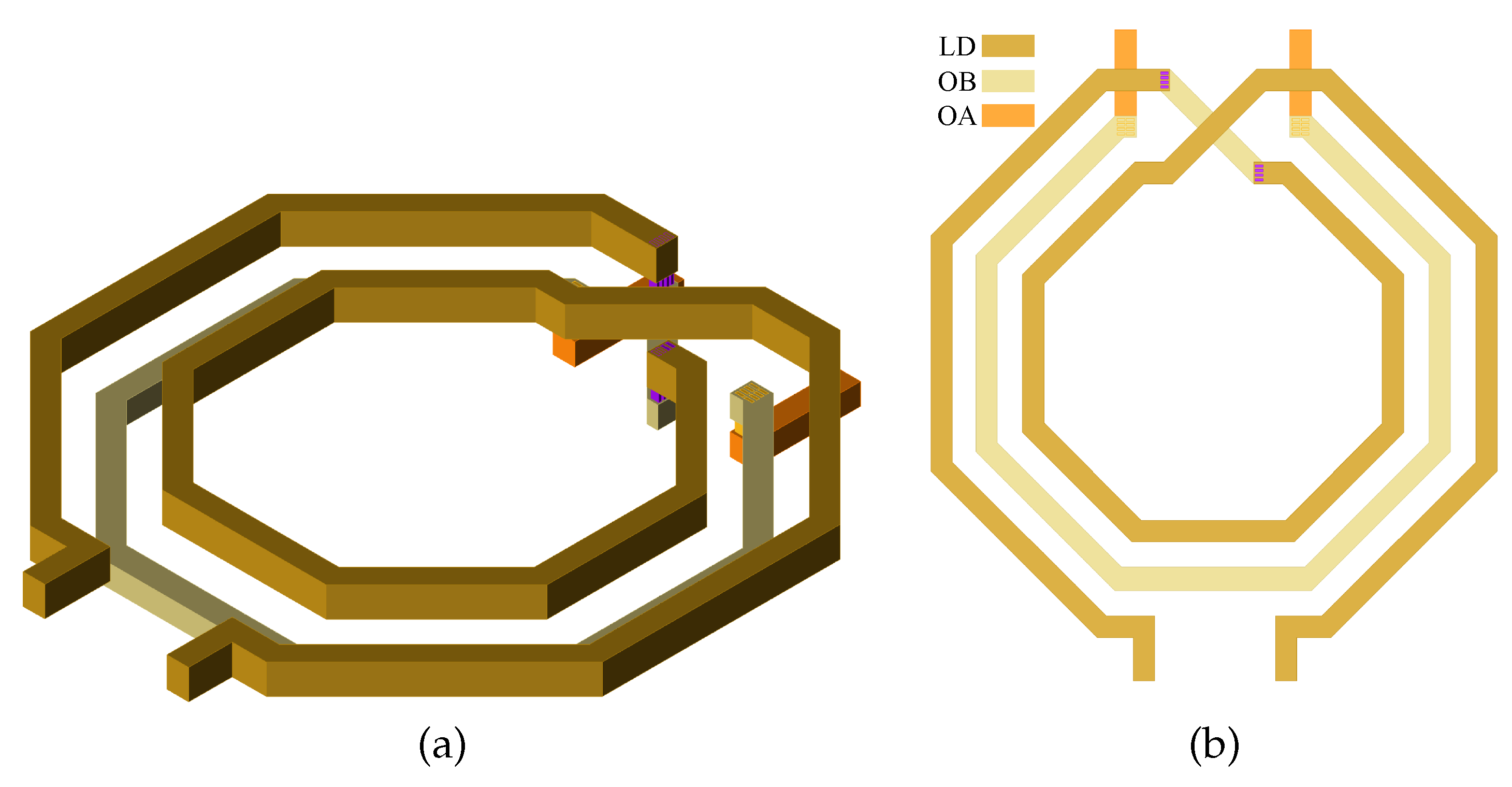
- Stacked Transformer (Figure 1): This configuration offers a high magnetic coupling, ranging from 0.6 to 0.8, but it also presents relatively large parasitic capacitances between the primary and secondary coils. Additionally, one coil must be on a lower metal layer than the other, which can affect the transformer’s Q.
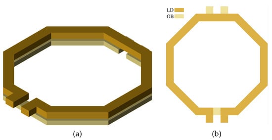 Figure 1. Stacked Transformer: 3D view (a) and 2D view (b).
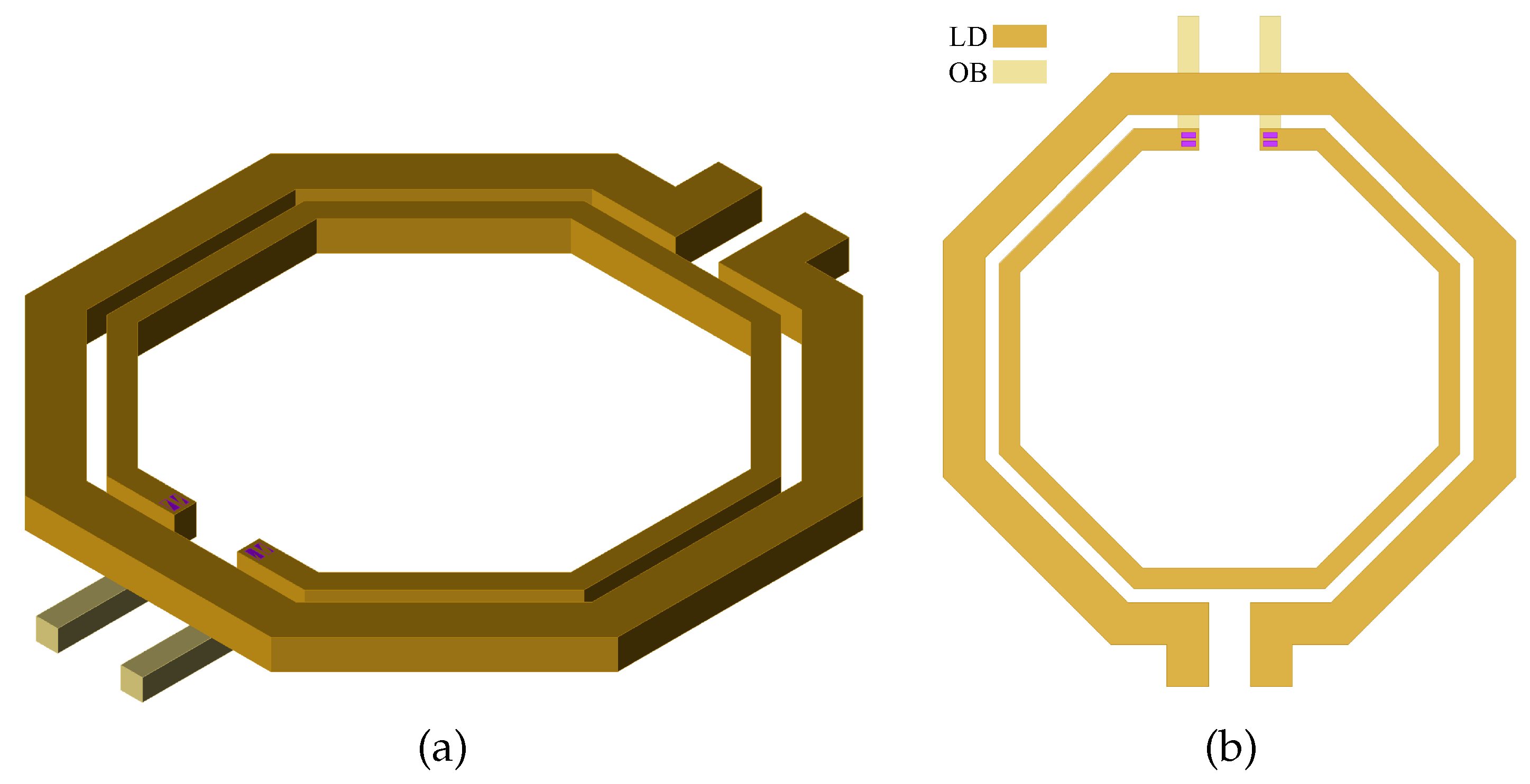
 - Coplanar Interwound Transformer (Figure 2): In this configuration, the primary and secondary coils are interwoven on the same metal layer, reducing parasitic capacitances but decreasing the magnetic coupling to a range of 0.5 to 0.7.
 Figure 2. Coplanar Interwound Transformer: 3D view (a) and 2D view (b).
 - Concentric Coplanar Transformer (Figure 3): In this configuration, both coils are arranged concentrically on the same metal layer, with one inside the other. This minimizes parasitic capacitances, but the magnetic coupling is the lowest, with values between 0.3 and 0.5. This is due to the fact that the mutual inductance is limited by the smaller cross section of the inner coil.
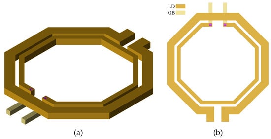 Figure 3. Concentric Coplanar Transformer: 3D view (a) and 2D view (b).
In our LNA design, a stacked octagonal transformer is designed due to its high coupling coefficient. As a result, the database will focus on this architecture.
3. Database Building and Searching Tool
The search tool is implemented as a MATLAB script that performs searches within a database containing the physical and electrical parameters of transformers and provides a graphical representation of their performance. The database comprises five data tables in .mat format, each containing information about the physical and electrical characteristics of various transformers. In each table, the rows represent different transformers, while the columns correspond to different frequencies, ranging from 1 GHz to 200 GHz in 1 GHz increments. The exception is the physical dimensions table, where each column represents a distinct physical parameter, radius (, ), track width (, ), and track spacing (s), as shown in Figure 4.
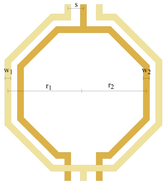
Figure 4.
Physical dimensions: radius (r1, r2), track width (w1, w2), and track spacing (s).
The methodology followed can be seen in Figure 5, which illustratively shows the entire process for the development of the database and the operation of the search tool.
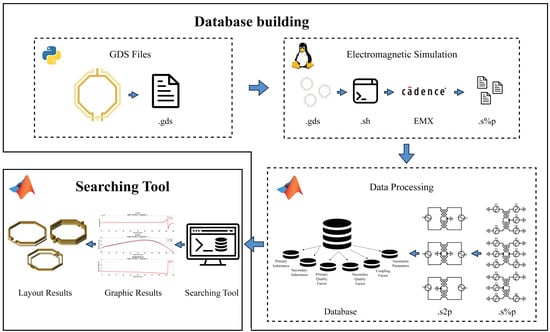
Figure 5.
Methodology. Generation of GDS files with Python 3.12.0, electromagnetic simulation with EMX (ElectroMagnetic eXtraction) through bash commands, and data processing with MATLAB R2023b and a MATLAB Searching Tool.
The methodology for database generation is illustrated in Figure 5. To build a database that allows for accurate searches, it is essential to include a large number of transformers. A Python script is used to generate the layout of thousands of transformers, supporting both four-sided and eight-sided designs. The script checks whether each transformer can be drawn based on the physical dimensions entered by the user as variables. If the transformer is feasible, it is drawn by calculating the points using trigonometric formulas based on the physical variables and connecting the segments, ultimately generating a .gds file. If the design is not feasible, the transformer is discarded, and the process continues with the next one.
To ensure each transformer is feasible, it is important to set constraints that prevent irregular designs. This is achieved through mathematical conditions applied at every stage of the generation process. The .gds extension refers to the GDSII (Graphic Database System) format, which is the industry standard for exchanging integrated circuit layouts and design data. This format allows for the representation of flat polygonal geometric shapes, text labels, and other design information in a hierarchical structure.
To create GDSII files, the tool uses the Python module gdspy, which facilitates the creation of these files and provides a set of functions for drawing polygons, holes, curves, circles, defining layers, and more. The tool operates by creating cells, within which the geometric elements are constructed and inserted. Additionally, it offers the capability to save, load, and use an internal viewer for files with the .gds extension.
The script allows for the addition of center taps and the configuration of metal layers for both the primary and secondary coils. Since a large number of layouts is required, the code can generate multiple layouts in a single execution, depending on the range and steps specified for each physical parameter of the transformer. It is worth noting that the name of each generated file contains information about its physical parameters, which will be used later by the MATLAB search tool.
To obtain the S-parameters for each transformer, the Cadence’s EMX software is used. Using this tool conventionally, through its graphical interface, would mean simulating the transformers one by one, which could take hours or even days. Therefore, the process is automated using a Bash script to execute the EMX tool for each transformer through a Linux terminal without the need to run Cadence. The Bash script specifies all the necessary information for parasitic extraction, such as the frequency range and steps, the path to the GDS file, the path to store the S-parameter file, and the path to the necessary technology files, such as the .proc file, which describes the technological properties and parameters of the fabrication process, including the metal layers. For each GDS file, a Touchstone file with the same name is generated. The Touchstone format is the industry standard for storing S-parameters and is the default format used by Cadence.
With the S-parameters of the transformers, it is necessary to calculate the electrical parameters to complete the construction of the database. However, the S-parameters generated by EMX are referenced to systems with SE ports. To fully characterize the transformer’s performance in a differential system, it is essential to convert these S-parameters into differential mode. This involves transforming the SE S-parameters into a balanced (differential) representation, which allows for the extraction of key electrical parameters such as the inductance, capacitance, and quality factor.
To convert a SE port structure into a differential port structure, the MATLAB RF Toolbox extension is used. This toolbox employs the formulations presented in [13]. A script is developed to convert the files from six and five ports to two differential ports as illustrated in Figure 6.
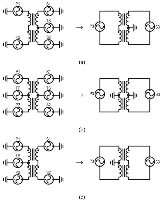
Figure 6.
Conversion of SE structures into differential structures: (a) secondary-tapped transformer with five SE ports into two differential ports, (b) dual-tapped transformer with six SE ports into two differential ports, and (c) primary-tapped transformer with five SE ports into two differential ports.
Once the transformation is complete, the electrical parameters are computed and stored in the database for future analysis and optimization. Equations (2)–(4) are used to calculate the inductances, quality factors, and coupling factor using Z-parameters derived from S-parameters through the MATLAB RF Toolbox function s2z. The calculation of the parameters is frequency specific, meaning they are determined for one frequency at a time. Therefore, to compute these parameters for, say, 200 frequencies for a single element, 200 individual calculations would be necessary, which, thanks to our script, would be performed automatically and subsequently stored in different tables that constitute the database. The script also extracts the physical dimensions of each transformer from the file name and then stores them in the database.
As mentioned earlier, the database is accessed through a search tool. To perform a search, the user needs to input the desired inductance for each stage of the transformer, the operating frequency, and an allowable percentage error, which is applied during the inductance search. Additionally, transformers that have reached resonance before the operating frequency are excluded, as a transformer is only useful below its self-resonant frequency (SRF). The search results are stored in a matrix, from which the necessary data are extracted to graphically display the electrical parameters, with the physical dimensions included as a reference in the legend.
4. A mm-Wave Differential LNA Designed Using the Database and Searching Tool
As an example of the tool’s application, a two-stage differential common-source (CS) LNA topology with two SE ports, as shown in Figure 7, is designed. This topology is utilized to achieve a very low NF through the use of inductive degeneration, specifically by employing coils in the transistors sources. The circuit comprises a total of three transformers, referred to as T, T, and T. The selection of the E band is due to the fact that passive components at lower frequencies exhibit excessively large sizes, whereas, as the frequency increases, they become smaller and more compact. Given the reduced size of the transformers in the developed database, this band is chosen as an optimal compromise and a representative example of modern applications. The LNA is designed for the mm-Wave band, specifically in the E band, in a range from 69.4 to 74.2 GHz. The circuit design is implemented in GlobalFoundries 45RFSOI technology. This technology features seven copper layers (M1–M3, C1, UA, OA, OB) and a top aluminum layer (LD).
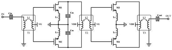
Figure 7.
Transformer-based matching networks LNA designed.
To begin designing the circuit, it is essential to size the transistor and select its physical characteristics. For this design, the Floating body NFET (rf_adnfet) model from the 45RFSOI technology is chosen due to the potential it has for PAs and LNAs design, featuring a gate width of 16 µm, 32 fingers, a gate length of 32 nm, and a multiplicity of 4. The multiplicity is modified to a value of four to divide the transistor into four sections, making the layout as square as possible and minimizing the total current flowing between the metal traces, thus improving the transistor’s NF. The transistor ports are physically interconnected through vertical connections to the passive elements in the upper layers as illustrated in Figure 8. The supply voltages and are set firstly to 342 mV as an optimal tradeoff to achieve minimal noise and low power consumption. The transistor is physically designed on the layers closest to the substrate, interconnected through vertical connections that connect the transistor ports to the passive elements in the upper layers as illustrated in Figure 8.
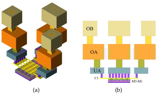
Figure 8.
A 3D view of the MOSFET used to design the LNA (a), and front view of the same device (b).
The design of the 408 mV LNA is achieved using a CS current density approach as detailed below. The active device demonstrates optimal noise performance at a current density, = 167.1921 A/µm. Consequently, the device achieves optimal noise performance when biased with a drain-source current, = 2.51 mA. Since the LNA comprises two cascaded CS stages, the nominal 0.9 V drain DC voltage required by the PDK can be reduced, and the gate DC voltage can be increased accordingly to maintain the same . This adjustment significantly reduces power consumption without substantially compromising LNA performance. Such optimization would not be feasible with a cascode topology. The DC supply voltage is reduced from 0.9 V to 408 mV, and the gate voltage is increased from 342 mV to 408 mV. With these values, the drain current remains at 2.51 mA as desired, ensuring minimal NF performance with negligible deviation in the gain and impedance matching of the LNA.
A MATLAB tool, based on the transformer-based impedance matching method outlined in [14], is utilized to compute the inductances of the transformers. The program generates various configurations for the matching network based on user-defined parameters, such as load impedance (Z), source impedance (Z), coupling factor, and operating frequency. These configurations incorporate a transformer along with auxiliary passive components, which may include inductors or capacitors arranged in series or parallel at any stage. Additionally, this method allows for the equalization of self-inductance, ensuring that both inductances have identical values. Table 1 presents the inductance values for each transformer at an operating frequency of 80 GHz.

Table 1.
Equalized inductances of the transformers extracted from the MATLAB tool.
The OA and OB layers are the most commonly used for the implementation of inductors and transformers, as they are the farthest from the substrate, thereby reducing parasitic capacitances. Both layers have the same thickness (3 µm), facilitating impedance equalization for the transformers. However, in this example, the OB and LD layers are utilized to further reduce parasitic capacitances and achieve a higher Q factor in the transformers.
To generate the database, approximately 20,000 transformers of each type (T, T, T) are simulated, resulting in a total of 60,000 transformers. The transformers are electromagnetically simulated over a frequency range from 1 GHz to 200 GHz, with a resolution of 1 GHz. Although this database is primarily developed for a circuit operating in the E-band, it can also be applied to other designs across various frequency bands. The simulations are performed on a Dell EMC PowerEdge R640 server, equipped with an Intel Xeon Gold 6240 processor (18 cores), 128 GB of RAM, 480 GB solid-state drive (SSD), and a 10 Gigabit Ethernet (GbE) network interface card (NIC). The server operates under the Red Hat Enterprise Linux 7 operating system. The total computational time for all simulations is approximately 144 h, with each transformer type requiring roughly 48 h of processing. For users with limited hardware resources, one adaptation could involve scaling the database to specific frequency bands or design requirements rather than simulating a broad range of transformers. As an example of the database developed in this article, it could be scaled by reducing the frequency range from 1–200 GHz with 1 GHz increments to 20–120 GHz with 2 GHz increments, while also decreasing the number of transformers per type from 20,000 to 5000, resulting in a total of 15,000 transformers instead of 60,000. This would significantly reduce the computational burden while still allowing users to benefit from the methodology. Although this approach requires a considerable amount of time, it is significantly more efficient than the conventional method of manually designing and iteratively simulating transformers. By executing the scripts a single time, all necessary electromagnetic simulations are performed, and the database is constructed, streamlining the process substantially. The resulting database provides a streamlined approach for optimal design, greatly simplifying and accelerating the process.
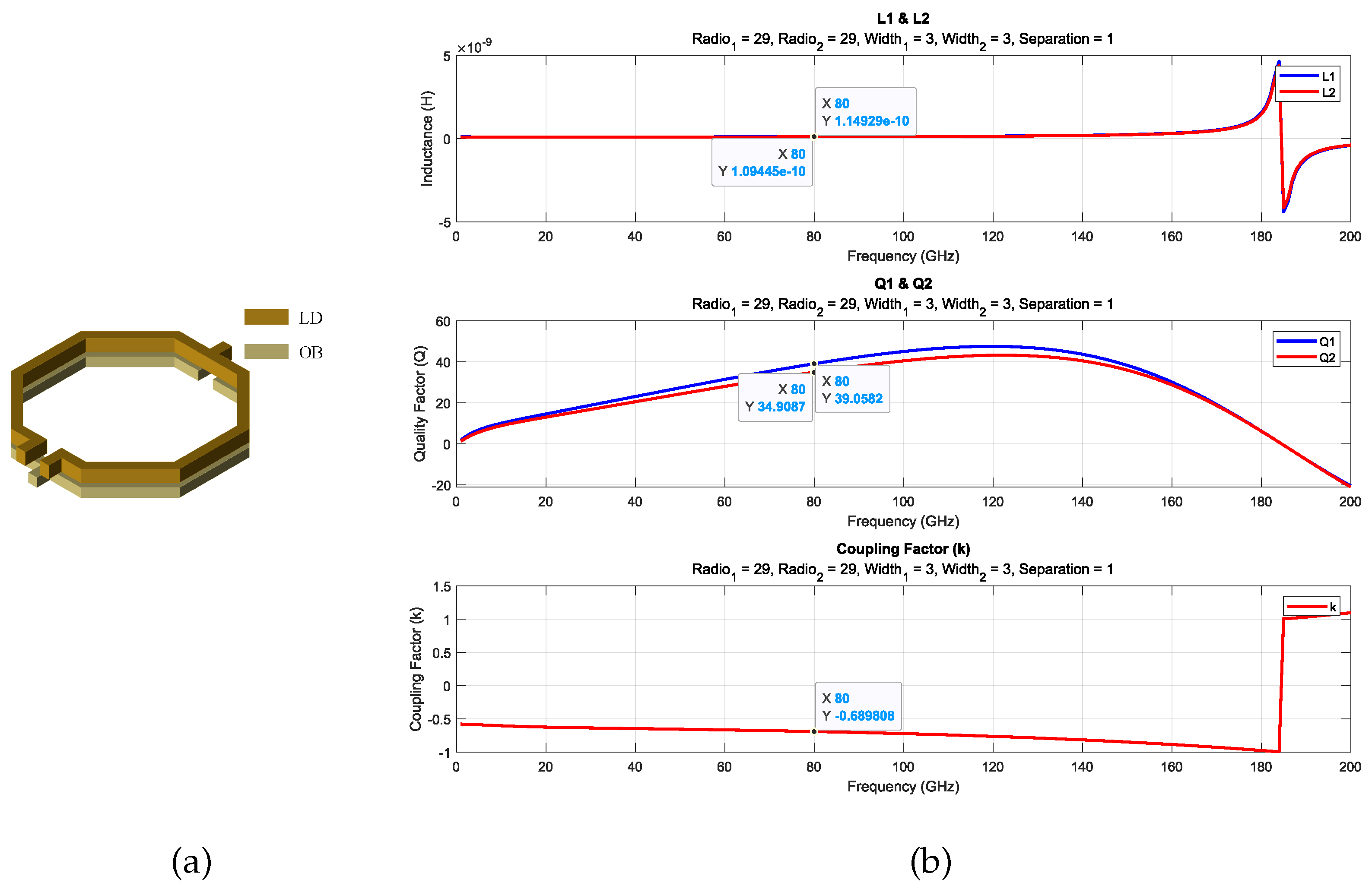
After constructing the database, the search tool is utilized to identify the transformers that best match the specified parameters, namely, the design frequency and target inductance. The selection process involves progressively reducing the percentage error in inductance until a transformer with an inductance sufficiently close to the desired value is identified. In cases where multiple transformers exhibit the same inductance, the transformer with the highest quality factor in the primary stage is chosen. Finally, the electrical parameters of each transformer identified through the search are presented graphically, providing a clearer understanding of their functionality. The results for transformers T, T, and T are shown in Figure 9, Figure 10 and Figure 11 and Table 2. This database serves as a highly effective tool, allowing designers to conduct targeted searches for transformers tailored to their specific requirements.
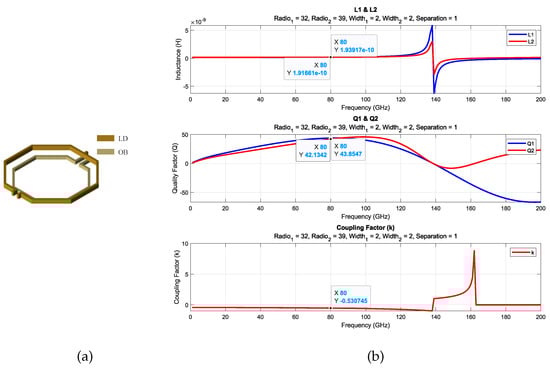
Figure 9.
A 3D view of T transformer (a) and electric parameters (b).
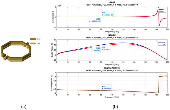
Figure 10.
A 3D view of T transformer (a) and electric parameters (b).
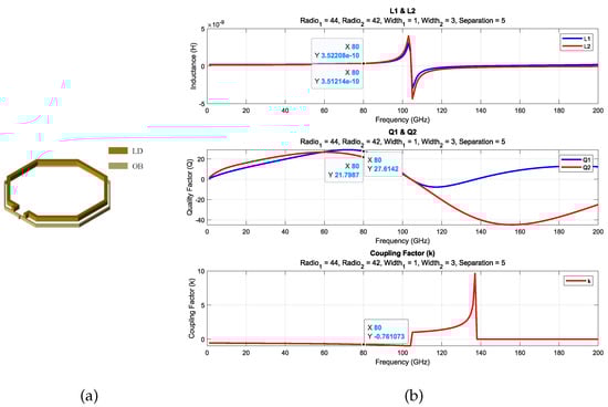
Figure 11.
A 3D view of T transformer (a) and electric parameters (b).
Table 2.
Transformers electric and physical parameters at 80 GHz.
As shown in Table 3, the results are very close, except for transformer T, where there is a difference of approximately 15 pH compared to the target values. This is because the desired inductance is quite small, and the database does not contain transformers of such small sizes to achieve an exact result. However, since the value is sufficiently close, it was decided to proceed with this value.
Table 3.
Inductances obtained from the database versus target inductances.
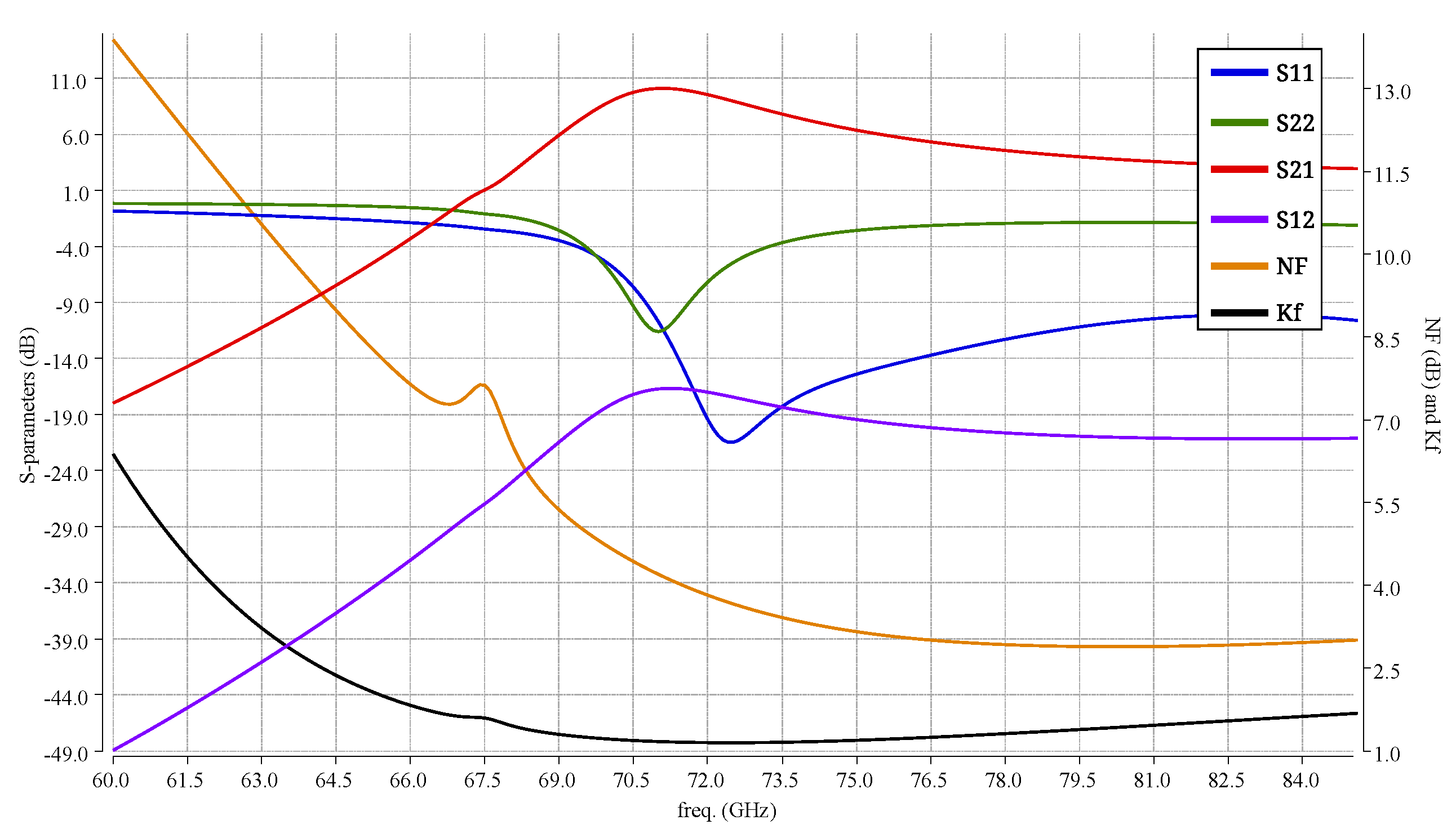
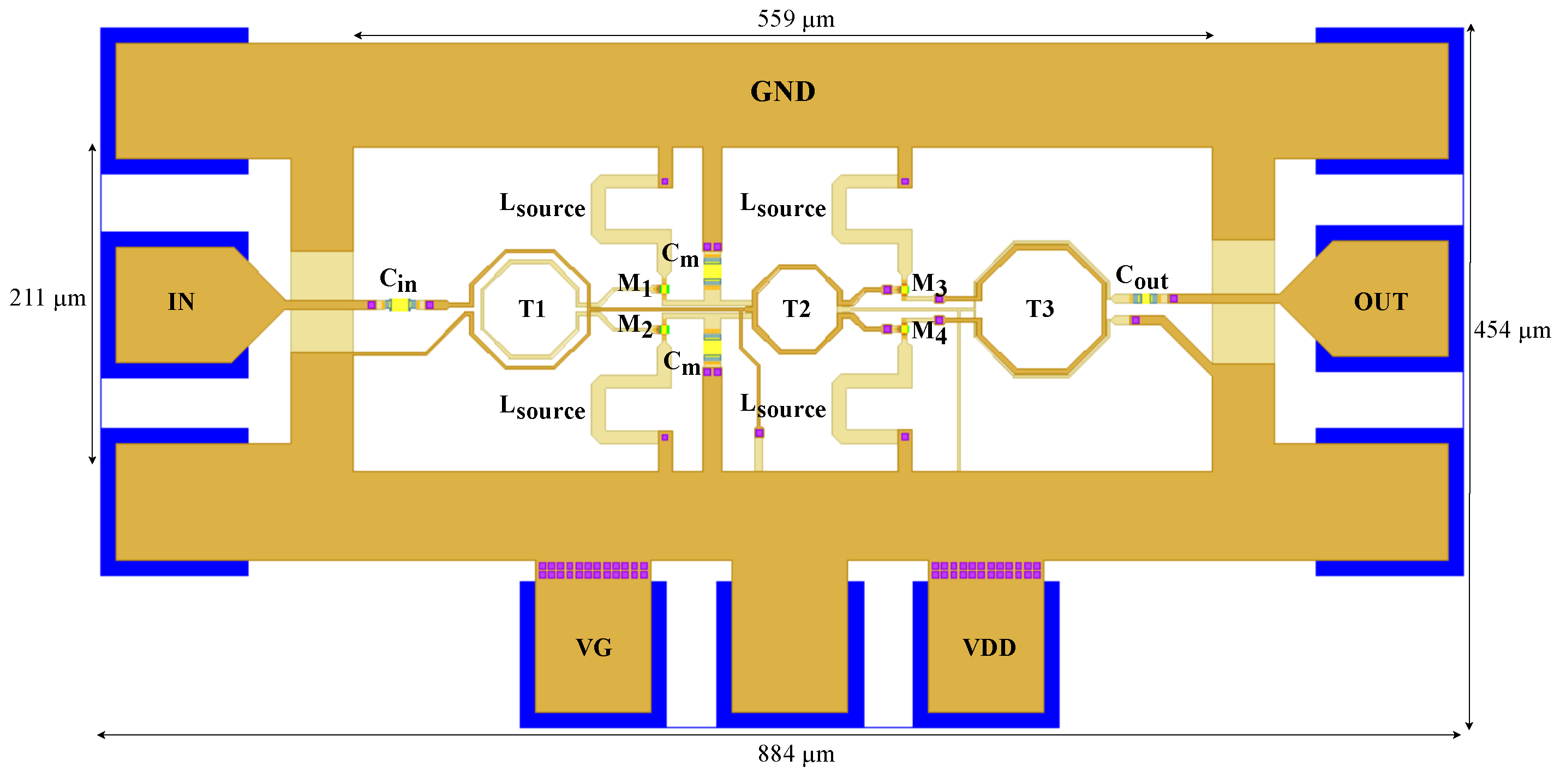
After obtaining the transformer layout quickly through the database, the symbol of the transformers containing their electromagnetic simulations is added. As shown in Figure 12, the S-parameters of the circuit are presented after the addition of the real model of the transistor and transformers. As a consequence of the transformer layout parasitics, the operating center frequency shifted from 80 GHz to 71.15 GHz. The designed LNA has a bandwidth of 4.8 GHz, ranging from 69.4 to 74.2 GHz, with a very low power consumption of 4.7 mW. A gain of 10.1 dB and an NF of 4.1 dB at 71.15 GHz is achieved, and the circuit is considered well matched, as it provides S and S values below −10 dB. The final layout is shown in Figure 13, occupying an area of 0.12 mm.
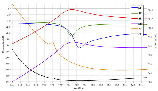
Figure 12.
Simulation results of the proposed LNA with the EM characterization of each passive component.
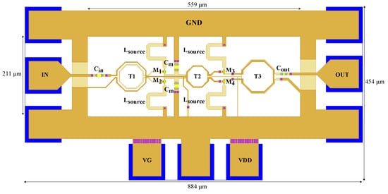
Figure 13.
Simplified top view of the differential LNA final layout.
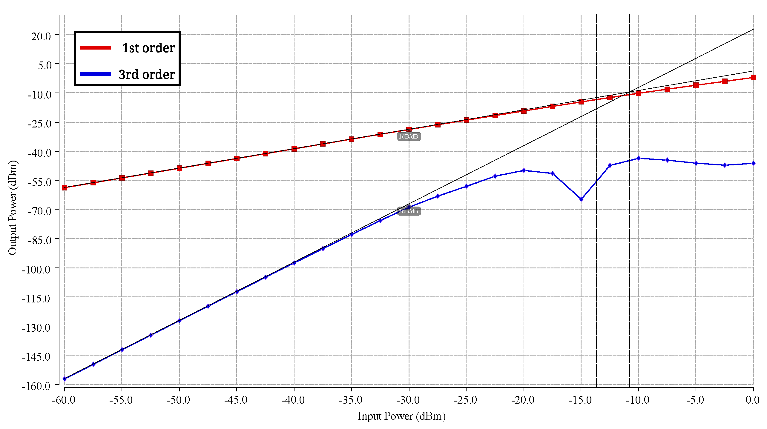
In addition, a study of the circuit’s linearity is conducted. Figure 14 illustrates the 1 dB compression (P) and IIP3 with 100 MHz spacing, with values of −13.7 dBm and −10.8 dBm, respectively.
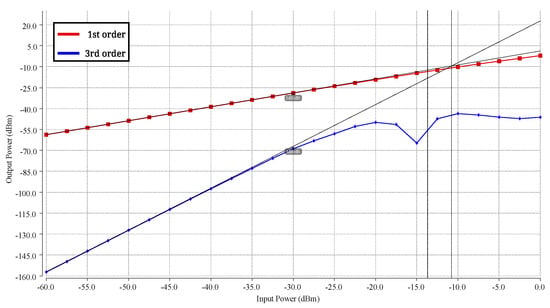
Figure 14.
Input and output third-order intercept of the developed LNA.
To validate the results, a 250-occurrence Monte Carlo simulation is conducted to assess whether the performance meets the specifications under all conditions. The histograms summarizing this analysis are presented in Figure 15a–d. As shown, the peak IRL (Figure 15a) and ORL (Figure 15b) exhibit mean values of 17.83 dB and 9.73 dB, respectively. The gain and NF of the LNA are illustrated in Figure 15c,d, demonstrating that the LNA achieves a mean gain value of 9.88 dB and a mean NF of 4.18 dB, both at 71.15 GHz.
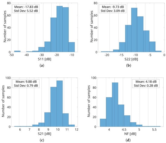
Figure 15.
Monte Carlo analysis results of the IRL (a), ORL (b), gain (c), and NF (d) of the proposed LNA.
Table 4 presents a comparison with several relevant circuits from the state of the art. In [8], the authors develop an LNA for the D-band (110–170 GHz) with four differential stages in CS configuration using 45 nm complementary metal–oxide–semiconductor (CMOS) SOI technology, achieving a gain of 16 dB and an NF of 8 dB, with a high power consumption of 75 mW and a bandwidth ranging from 125.5 to 157 GHz. Another LNA designed in 65 nm CMOS SOI technology for the Ka-band, with a bandwidth of 34.5 to 44.5 GHz, is presented in [15]. It features two differential stages in CS configuration, offering an NF of 3.2 dB and a gain of 20.5 dB, with a consumption of 22.3 mW. In [10], an LNA for the E-band (65–90 GHz) in 45 nm CMOS SOI technology is shown, with two differential CS stages, achieving a gain of 8.9 dB and an NF of 3.2 dB, along with a low power consumption of 6.75 mW. Reference [16] presents an LNA in 55 nm CMOS with a bandwidth of 64–84 GHz and three differential stages in CS configuration, offering an NF of 5.1 dB and a gain of 11.8 dB, with a high power consumption of 40 mW. Finally, ref. [17] features an LNA with two differential CS stages, operating within a bandwidth of 57.8–67 GHz, providing an NF of 3.1 dB and an excellent gain of 20.7 dB but with a high consumption of 21 mW. To conduct a comparative analysis of the obtained results against the state of the art, a figure of merit (FoM) is utilized fairly, employing Equation (5) for its calculation, where F represents the minimum noise factor, G denotes the maximum linear gain, and denotes the power consumption (mW):
Table 4.
Overview of similar state-of-art LNAs with the proposed circuit.
It can be observed that the designed circuit possesses the highest FoM among all the compared works. The only circuit with a comparable FoM is the work presented in [17], which achieves double the gain compared to our design but at the expense of very high power consumption. Our circuit not only stands out for having the best FoM but also for the methods employed to achieve this performance. Besides all the design decisions made, the development of the database and the search tool are fundamental elements not only for the design process itself but also for its optimization and time reduction, demonstrating their effectiveness in developing designs that utilize transformers.
5. Conclusions
The development of a tool capable of streamlining the transformer design process for any circuit is presented in this work. This tool can automatically create a database containing information about the physical and electrical parameters of thousands of transformers. Compared to existing tools, such as those offered by PDKs or artificial intelligence-based solutions, the developed database provides enhanced precision and flexibility, as it imposes no restrictions on transformer structures. To achieve this, a Python program was developed to generate the GDS files required for electromagnetic simulations. Additionally, a Linux script was created to automate the execution of all EMX electromagnetic simulations. Finally, two MATLAB scripts were implemented: one for constructing the database and another for searching within it to select the desired transformer. This database allows users to conduct searches based on specified input parameters, returning a list of transformers that meet the defined characteristics. The database was created in approximately 144 h, includes 60,000 transformers, and can be leveraged for other designs. To validate the tool, a differential LNA for mm-Wave applications was designed using 45RFSOI technology. The main innovation of the designed LNA lies in the methodology used for designing the transformers, as the database allows finding a transformer that fits the design requirements in a matter of seconds. The presented LNA achieved a gain of 10.1 dB and an NF of 4.1 dB, consumed a total power of 4.7 mW from a 0.406 mV DC supply, and occupied an area of 0.12 mm excluding pads. Although the proposed circuit provides excellent performance, the main highlight of our contribution is the development of a tool for finding optimal transformer parameters given a certain circuit topology. With the proposed method, the design time is optimized by eliminating the need for manual custom transformer design, as opposed to state-of-art LNAs. Although this article focused on designing an LNA to validate the tool’s functionality, the developed database is entirely reusable for any circuit requiring transformers due to its ability to perform parameter-based searches and identify a transformer that meets the desired inductance at a specific operating frequency.
Author Contributions
Methodology, J.d.P., S.K., J.T.-C. and N.M.-C.; Investigation, J.d.P., S.K., J.T.-C. and N.M.-C.; Supervision, J.d.P., S.K. and D.G.-S.; Writing—original draft, J.T.-C. and N.M.-C.; Writing—review and editing, J.d.P., S.K. and D.G.-S.; Visualization, J.T.-C. and N.M.-C.; Project administration, J.d.P. and S.K.; Funding acquisition, J.d.P. and S.K. All authors have read and agreed to the published version of the manuscript.
Funding
This work has been partially supported by the Spanish Ministry of Science and Innovation (MCIN) and the Research State Agency (AEI) as part of the project with ID PID2021-127712OB-C21/MCIN/AEI/10.13039/501100011033/FEDER, EU, and PDC2023-145828-C22/MCIN/AEI/10.13039/501100011033/NextGenerationEU.
Data Availability Statement
The data presented in this study are available on request from the corresponding author.
Conflicts of Interest
The authors declare no conflicts of interest.
Abbreviations
The following abbreviations are used in this manuscript:
| Balun | Balanced to Unbalanced |
| BW | Bandwidth |
| CMOS | Complementary Metal Oxide Semiconductor |
| CS | Common Source |
| EMX | Electromagnetic Extraction |
| FoM | Figure of Merit |
| GbE | Gigabit Ethernet |
| GDSII | Graphic Database Stream |
| IIP3 | Third-Order Intercept Point |
| IRL | Input Return Loss |
| P | 1 dB Compression Point |
| LNA | Low-Noise Amplifier |
| mm-Wave | Millimeter Wave |
| NF | Noise Figure |
| NIC | Network Interface Card |
| ORL | Output Return Loss |
| PA | Power Amplifier |
| Q | Quality Factor |
| RF | Radio Frequency |
| RFIC | Radio Frequency Integrated Circuit |
| SE | Single Ended |
| SSD | Solid-State Driver |
| SOI | Silicon On Insulator |
| SRF | Self-Resonant Frequency |
| VCO | Voltage-Controlled Oscillator |
References
- Niknejad, A.M.; Meyer, R.G. Analysis, design, and optimization of spiral inductors and transformers for Si RF ICs. IEEE J. Solid-State Circuits 1998, 33, 1470–1481. [Google Scholar] [CrossRef]
- Niknejad, A.M.; Meyer, R.G. Analysis of eddy-current losses over conductive substrates with applications to monolithic inductors and transformers. IEEE Trans. Microw. Theory Tech. 2001, 49, 166–176. [Google Scholar] [CrossRef]
- Ng, K.T.; Rejaei, B.; Burghartz, J.N. Substrate effects in monolithic RF transformers on silicon. IEEE Trans. Microw. Theory Tech. 2002, 50, 377–383. [Google Scholar] [CrossRef]
- Mohan, S.S.; Yue, C.P.; del Mar Hershenson, M.; Wong, S.S.; Lee, T.H. Modeling and characterization of on-chip transformers. In Proceedings of the International Electron Devices Meeting 1998. Technical Digest (Cat. No. 98CH36217), San Francisco, CA, USA, 6–9 December 1998; pp. 531–534. [Google Scholar]
- Koutsoyannopoulos, Y.K.; Papananos, Y. Systematic analysis and modeling of integrated inductors and transformers in RF IC design. IEEE Trans. Circuits Syst. II Analog. Digit. Signal Process. 2000, 47, 699–713. [Google Scholar] [CrossRef]
- Zolfaghari, A.; Chan, A.; Razavi, B. Stacked inductors and transformers in CMOS technology. IEEE J. Solid-State Circuits 2001, 36, 620–628. [Google Scholar] [CrossRef]
- Fong, N.; Plouchart, J.O.; Zamdmer, N.; Kim, J.; Jenkins, K.; Plett, C.; Tarr, G. High-performance and area-efficient stacked transformers for RF CMOS integrated circuits. In Proceedings of the IEEE MTT-S International Microwave Symposium Digest, Philadelphia, PA, USA, 8–13 June 2003; Volume 2, pp. 967–970. [Google Scholar]
- Hamani, A.; Siligaris, A.; Blampey, B.; Dehos, C.; Jimenez, J.L.G. A 125.5–157 GHz 8 dB NF and 16 dB of gain D-band low noise amplifier in CMOS SOI 45 nm. In Proceedings of the 2020 IEEE/MTT-S International Microwave Symposium (IMS), Los Angeles, CA, USA, 4 August–30 September 2020; pp. 197–200. [Google Scholar]
- Liao, S.; Guo, G.; Liu, H.; He, W. Design of a 30–40 GHz Low-Noise Amplifier in 45 nm SOI Technology. In Proceedings of the 2023 IEEE MTT-S International Microwave Workshop Series on Advanced Materials and Processes for RF and THz Applications (IMWS-AMP), Leuven, Belgium, 11–13 September 2023; pp. 1–3. [Google Scholar]
- Reyna, D.F. Diseño De Un Lna Integrado Para Banda E Con Redes De Adaptacion De Impedancias Mediantes Transformadores. 2023. Available online: http://hdl.handle.net/10553/125692 (accessed on 1 February 2024).
- Passos, F.; Lourenço, N.; Roca, E.; Martins, R.; Castro-López, R.; Horta, N.; Fernández, F.V. PACOSYT: A passive component synthesis tool based on machine learning and tailored modeling strategies towards optimal RF and mm-Wave circuit designs. IEEE J. Microw. 2023, 3, 599–613. [Google Scholar] [CrossRef]
- Bevilacqua, A. Fundamentals of integrated transformers: From principles to applications. IEEE Solid-State Circuits Mag. 2020, 12, 86–100. [Google Scholar] [CrossRef]
- Frickey, D.A. Conversions between S, Z, Y, H, ABCD, and T parameters which are valid for complex source and load impedances. IEEE Trans. Microw. Theory Tech. 1994, 42, 205–211. [Google Scholar] [CrossRef]
- Lançon, L.; Vallée, H.; Montoriol, G.; Brunelli, F.; Taris, T. Integrated-Transformer-Based Impedance Matching Method: Impedance Matching With Transformers. IEEE Microw. Mag. 2022, 23, 40–56. [Google Scholar] [CrossRef]
- Yu, M.; Wen, J. An analytical approach to designing millimeter-wave LNAs with transformer-based matching networks. Microw. Opt. Technol. Lett. 2024, 66, e34066. [Google Scholar] [CrossRef]
- Zhang, X.; Shi, C.; Zhang, R.; Deng, H.; Chen, J. A 64–84 GHz CMOS LNA with Excellent Gain Flatness for Wideband mmW Applications. In Proceedings of the 2021 IEEE International Symposium on Circuits and Systems (ISCAS), Daegu, Republic of Korea, 22–28 May 2021; pp. 1–5. [Google Scholar]
- Eltaliawy, A. CMOS Front-End Circuits in 45-nm SOI Suitable for Modular Phased-Array 60-GHz Radios. 2021. Available online: http://hdl.handle.net/10012/16734 (accessed on 5 February 2024).


Disclaimer/Publisher’s Note: The statements, opinions and data contained in all publications are solely those of the individual author(s) and contributor(s) and not of MDPI and/or the editor(s). MDPI and/or the editor(s) disclaim responsibility for any injury to people or property resulting from any ideas, methods, instructions or products referred to in the content. |
© 2025 by the authors. Licensee MDPI, Basel, Switzerland. This article is an open access article distributed under the terms and conditions of the Creative Commons Attribution (CC BY) license (https://creativecommons.org/licenses/by/4.0/).