Article

The Intrinsic Mechanism and Suppression Strategy of Transient Current Imbalance Among Parallel Converters

1
School of Electrical & Electronic Engineering, Hubei University of Technology, Wuhan 430068, China
2
School of Electrical & Electronic Engineering, Huazhong University of Science and Technology, Wuhan 430074, China
*
Author to whom correspondence should be addressed.
Electronics 2025, 14(4), 714; https://doi.org/10.3390/electronics14040714
Submission received: 20 January 2025 / Revised: 6 February 2025 / Accepted: 10 February 2025 / Published: 12 February 2025
(This article belongs to the Topic Advances in Power Science and Technology, 2nd Edition)

Abstract

:
Due to the difficulty in achieving a high-power output with a single converter, parallel converters are widely used in high-power applications. However, inconsistency in the output voltage feedback coefficients of individual converters and the associated dispersion in parallel systems often lead to unbalanced current sharing during transient processes, such as load disturbances. This imbalance can result in certain converters being overloaded during transients, leading to premature shutdown. Subsequently, the load on the remaining converters increases, further aggravating the imbalance and triggering additional shutdowns in a domino effect, which may, ultimately, cause the entire parallel converter system to shut down. To address this issue, this study focuses on parallel phase-shift full-bridge systems, analyzing the intrinsic mechanism by which feedback coefficient dispersion affects transient current sharing. A droop control strategy with improved transient virtual impedance is proposed to enhance the current sharing during transients. A simulation and experimental results demonstrate that the proposed strategy significantly improves current sharing during transient processes, effectively enhancing the dynamic performance and reliability of the system.

1. Introduction

As fossil fuels face both economic and environmental challenges, the demand for energy supply continues to grow. DC/DC converters, as a core component of energy conversion, have seen widespread applications across various fields [1,2,3,4,5]. The most commonly used DC/DC converters are primarily classified into isolated and non-isolated types. Non-isolated converters include Buck, Boost, and H-bridge converters. The Buck converter is characterized by its simple structure, high efficiency, and low cost, making it widely used in step-down voltage conversion [6,7,8]. The Boost converter is capable of converting a low input voltage to a higher output voltage, typically exhibiting high efficiency and a simple structure [9,10]. The H-bridge converter supports the bidirectional energy flow control, features a simple structure, and is easy to design [11,12].
Isolated converters include LLC, DAB, and Phase-Shift Full-Bridge (PSFB) converters. LLC converters can achieve Zero Voltage Switching (ZVS) and Zero Current Switching (ZCS), effectively reducing switching losses, though their parameter design is relatively complex [13,14,15]. DAB converters support the bidirectional power flow and offer a high power density. However, due to the need for more switching devices, its cost is relatively high [16,17,18]. The phase-shift full-bridge (PSFB) converter has been widely adopted in medium- and high-power applications due to its advantages of a simple structure, a high power density, and low electromagnetic interference (EMI) [19,20,21,22,23,24], and with the continuous expansion of medium-voltage DC power supply systems, single DC converters have become insufficient to meet the increasing power transmission demands. Consequently, the parallel operation of multiple converters has gradually emerged as a common and efficient solution.
Parallel systems have been widely utilized in fields such as telecommunication systems, marine electric propulsion, and distributed power systems due to their advantages of high reliability, redundancy, and ease of modular expansion [25,26,27,28,29]. However, dispersion in the main circuit and control parameters of practical converters makes it difficult for parallel converters to maintain fully consistent characteristics. These minor parameter deviations can easily cause unbalanced current sharing, which adversely affects the performance and stability of the parallel system [30]. To achieve proper current sharing among parallel converters, certain current sharing control strategies are typically required.
To date, many researchers have proposed various methods for current sharing in parallel converters, primarily including droop control, master–slave control, and external controller methods, with further improvements to enhance the current sharing performance. Reference [31] analyzed the influence of line impedance on droop control in parallel systems, which leads to output voltage mismatches and circulating currents, and proposed an adaptive droop control strategy with real-time impedance estimation. Reference [32] addressed the uneven load sharing and insufficient voltage regulation accuracy of traditional droop control by introducing improved voltage compensation and variable droop control strategies. Reference [33] adopted a communication between adjacent modules to achieve decentralized parallel converter operation without centralized control. Reference [34] proposed a linear quadratic regulator (LQR) with integral action based on master–slave control, incorporating current control and dynamic model identification using recursive least squares. Reference [35] introduced a distributed control method to achieve proportional load sharing based on locally measured control strategies. References [36,37] improved the droop control by utilizing sliding mode control to enhance the response speed and voltage regulation performance. However, the chattering phenomenon inherent in the sliding mode control can compromise the system’s reliability and lifespan. Reference [38] addressed the load sharing imbalances caused by sensor errors in parallel systems and proposed a novel nonlinear droop control technique that can adaptively adjust the output of distributed generation units. Reference [39] considered the impact of transformer turns ratio differences and inductance discrepancies on parallel systems and proposed a dynamic hybrid compensator (DHC) based on a master–slave control. However, these methods primarily focus on optimizing the current sharing performance during the steady-state operation of parallel systems. The impact of parameter dispersion on the transient characteristics of parallel converters has not been thoroughly investigated. In certain power applications, converters must be capable of handling significant load variations, making transient performance a critical consideration.
In high-power applications, voltage loop control for individual converters is commonly employed to achieve miniaturization, a lightweight design, and the cost control of converter modules. However, if discrepancies exist in the output voltage feedback coefficients of parallel converters, they can significantly impact transient current sharing during dynamic processes such as sudden load increases. This may render the parallel system incapable of effectively handling rapid load changes. Some converters may withstand current surges far exceeding their rated values, triggering protective mechanisms and making the converters shut down. This not only undermines the overall system reliability but also risks damaging the converters themselves. The novelty of this study lies in the in-depth analysis of the impact of output voltage feedback coefficient discrepancies on the transient characteristics of parallel converter systems and the proposal of an improved control strategy to optimize the transient current imbalances caused by these discrepancies.
In this study, a state–space model of two IPOS phase-shift full-bridge converter systems based on droop control is first established, and the impact of the differences in output voltage feedback coefficients on the system’s dynamic characteristics is analyzed. On this basis, an improved virtual impedance control strategy is proposed to enhance the dynamic performance of the system under conditions of feedback coefficient discrepancies, and the effects of this strategy on the system’s stability are investigated.
The structure of this paper is as follows: Section 2 establishes a state–space model of parallel IPOS phase-shift full-bridge converters. Section 3 investigates the influence of output voltage feedback coefficient discrepancies on the transient performance of the parallel system. Section 4 proposes an improved virtual impedance control strategy and analyzes its effectiveness in optimizing transient performance and stability. Section 5 validates the proposed method through simulations and experiments.

2. State–Space Model of Parallel Interleaved Phase-Shift Full-Bridge Converters

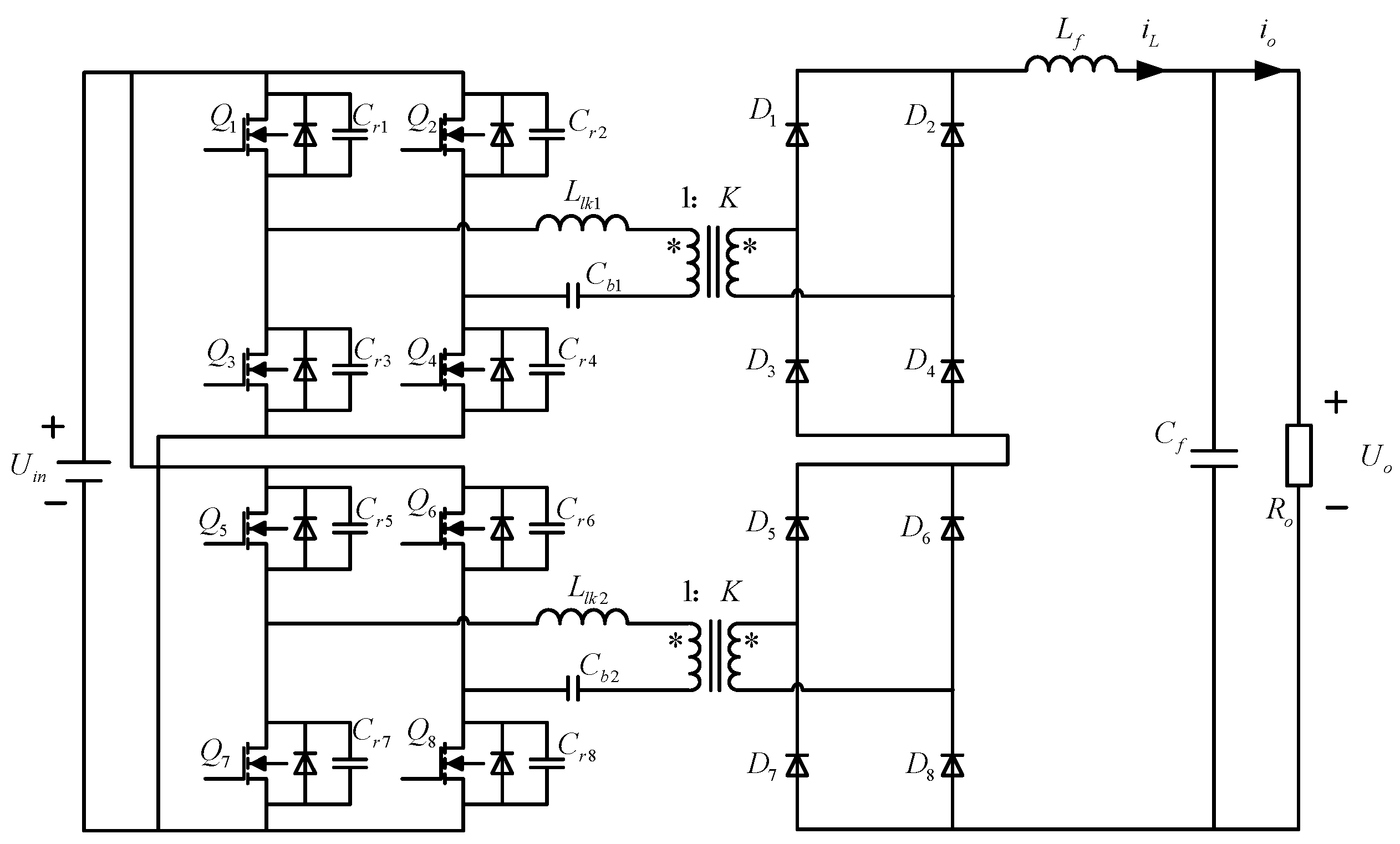
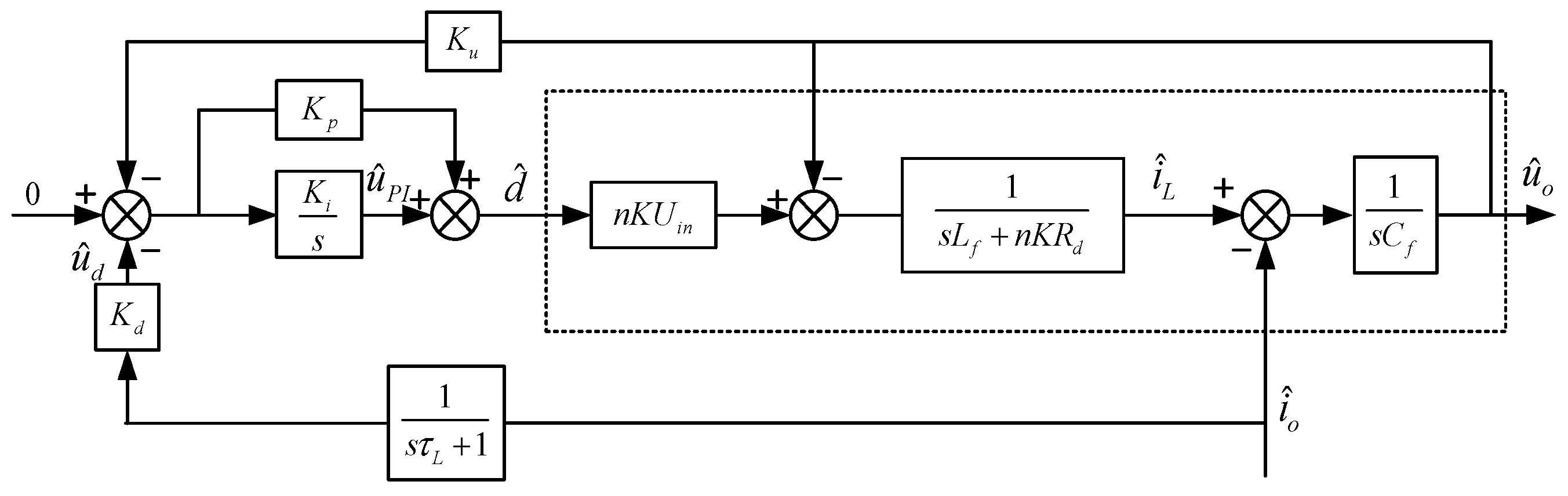
2.1. Modeling of Single-Module IPOS Phase-Shifted Full-Bridge System

To analyze the dynamic process of load transients in a parallel phase-shift full-bridge system with differences in output voltage feedback coefficients, a mathematical model of a single-module IPOS phase-shift full-bridge control system is first established. On this basis, a mathematical model of a parallel system comprising two IPOS phase-shift full-bridge converters is developed. The topology of the single-module IPOS phase-shift full-bridge converter is shown in Figure 1. It consists of two phase-shift full-bridge converters, with the inputs connected in parallel and the outputs connected in series. The PWM signals of the two phase-shift full-bridge modules have a certain phase difference. This structure is suitable for applications with low-voltage, high-current inputs and high-voltage, low-current outputs [40]. In Figure 1, Q 1 ~ Q 8 are the switching devices; C r 1 ~ C r 8 are the parasitic capacitances of the switches; D 1 ~ D 8 represent the rectifier diodes; K is the transformer turns ratio; L l k 1 , L l k 2 are the leakage inductances of the transformers; L f is the filter inductance; C f is the filter capacitance; R o is the load resistance; U i n is the input voltage; U o is the output voltage; i L is the inductor current; and i o is the output current.
According to [41], the small-signal mathematical model of the IPOS phase-shift full-bridge system is shown in Figure 2, where n represents the number of phase-shift full-bridge modules in a single IPOS converter; here, n = 2. d ^ represents the small disturbance of the duty cycle; i ^ L represents the small disturbance of the inductor current; i ^ o represents the small disturbance of the output current; and u ^ o represents the small disturbance of the output voltage. R d = 4 K L l k f s + 4 C r U i n 2 f s K I L 2 , where f s is the switching frequency.
In parallel converter systems, certain current sharing control methods are typically employed to ensure an equal current distribution among the parallel converters. Due to its simplicity and lack of need for inter-module communication, droop control is widely applied. This method introduces a virtual resistance into the control loop to adjust the external characteristics of the parallel system, achieving current sharing without additional power loss [42,43,44,45,46,47]. To investigate the impact of output voltage feedback coefficients on the dynamic performance of the system, Figure 3 shows a control block diagram of a single-voltage-loop IPOS phase-shift full-bridge converter based on droop control. In Figure 3, the dashed box represents the small-signal mathematical model of the IPOS phase-shift full-bridge converter. The droop value in the droop control is derived from the low-frequency component of the output current filtered by a low-pass filter. Here, a first-order low-pass filter is used, with a cutoff frequency of ω L = 1 / τ L . K d represents the droop coefficient. K u represents the output voltage feedback coefficient. K p is the proportional gain of the voltage loop PI controller, and K i is the integral gain of the voltage loop PI controller.
Based on Figure 3, the following can be obtained:
i ^ L = n K U i n [ K p ( K u u ^ o u ^ d ) + u ^ P I ] u ^ o s L f + n K R d
u ^ P I = K i s ( K u u ^ o u ^ d )
u ^ d = K d s τ L + 1 i ^ o
u ^ o = i ^ L i ^ o s C f
To investigate the impact of load changes on the transient characteristics of the system, the output load resistance is considered an independent variable. The output current is then expressed as follows:
i ^ o = 1 R u ^ o u o R 2 R ^
Equations (3) and (4) can be expressed as follows:
u ^ d = K d s τ L + 1 ( 1 R u ^ o u o R 2 R ^ )
u ^ o = 1 s C f ( i ^ L 1 R u ^ o + u o R 2 R ^ )
To establish a state–space model of a single IPOS phase-shift full-bridge control system, the state variables are selected as the inductor current disturbance i ^ L , the output of the integrator in the voltage loop PI controller u ^ P I , the droop term derived from the low-frequency component after low-pass filtering multiplied by the droop coefficient u ^ d , and the output voltage disturbance u ^ o , namely, x 1 = [ i ^ L   u ^ P I   u ^ d   u ^ o ] T . To analyze the impact of load transients on the transient performance of the system, the disturbance of the output load resistance is selected as the input variable, namely, u = [ R ^ ] . The output current and output voltage disturbance are selected as the output variables, namely, y 1 = [ i ^ o   u ^ o ] T .
Further, the state–space model of the single-module IPOS phase-shift full-bridge can be expressed as follows: x 1 · = A 1 x 1 + B 1 u , y 1 = C 1 x 1 + D 1 u [48,49], where the system matrix A 1 , control matrix   B 1 , output matrix   C 1 , and direct transmission matrix D 1 are as follows:
A 1 = n K R d L f n K U i n L f n K U i n K p L f 1 n K U i n K p K u L f 0 0 K i K i K u 0 0 1 τ L K d τ L R 1 C f 0 0 1 R
B 1 = 0 0 K d u o τ L R 2 u o R 2 C f
C 1 = 0 0 0 1 R 0 0 0 1
D 1 = u o R 2 0

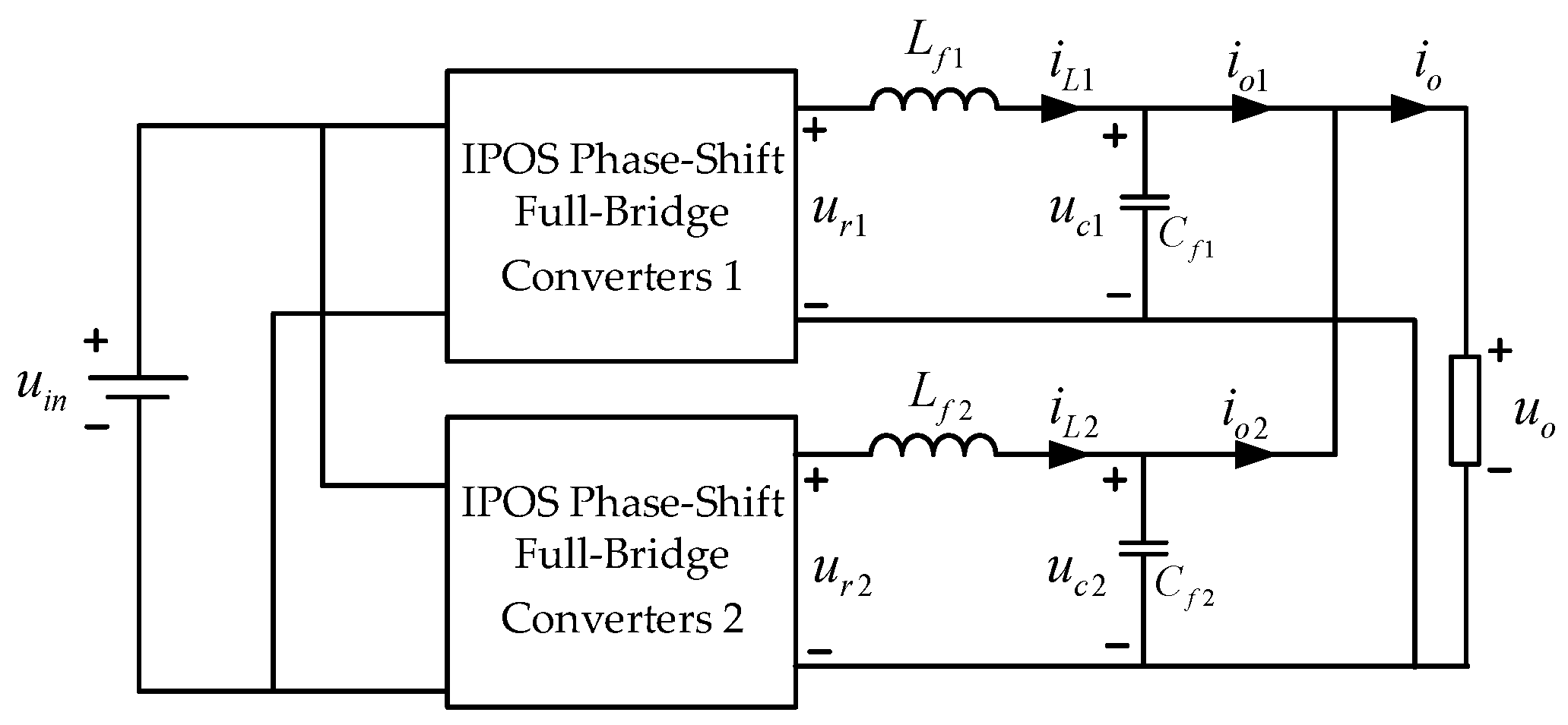
2.2. Model of a Parallel System with Two IPOS Phase-Shift Full-Bridge Converters

The parallel system with two IPOS phase-shift full-bridge converters consists of two single-module IPOS phase-shift full-bridge converters connected in parallel at both the input and output sides, as shown in Figure 4.
At the output side, the converters are connected in parallel, and their capacitors are also paralleled, resulting in the capacitor voltage being equal to the output voltage, namely, u c 1 = u c 2 = u o . Based on the derivation for a single converter, a state–space model for the parallel system of two converters is established. The selected state variables are the inductor currents of the two converters i ^ L 1 and i ^ L 2 , the outputs of the voltage loop integrators u ^ P I 1 and u ^ P I 2 , the droop terms after low-pass filtering and multiplication by the droop coefficients u ^ d 1 and u ^ d 2 , and the output voltage u ^ o , namely, x P = [ i ^ L 1   i ^ L 2   u ^ P I 1   u ^ P I 2   u ^ d 1   u ^ d 2   u ^ o ] T . Similarly, the input variable is selected as the disturbance of the load resistance, namely, u = [ R ^ ] . The output variables are the output voltage, the output currents of each converter, and the total output current, namely, y P = [ u ^ o   i ^ o 1   i ^ o 2   i ^ o ] T . From Figure 4, the following relationships can be derived:
C f 1 d u o d t = i L 1 i o 1 C f 2 d u o d t = i L 2 i o 2
L f 1 d i L 1 d t = u r 1 u o L f 2 d i L 2 d t = u r 2 u o
Based on the derivation process for a single converter, the relationships among the state variables for the parallel converter system can be expressed as follows:
i ^ L 1 = n K U i n [ K p ( K u 1 u ^ o u ^ d 1 ) + u ^ P I 1 ] u ^ o s L f + n K R d
i ^ L 2 = n K U i n [ K p ( K u 2 u ^ o u ^ d 2 ) + u ^ P I 2 ] u ^ o s L f + n K R d
u ^ P I 1 = K i s ( K u 1 u ^ o u ^ d 1 )
u ^ P I 2 = K i s ( K u 2 u ^ o u ^ d 2 )
u ^ d 1 = K d s τ L + 1 i ^ o 1
u ^ d 2 = K d s τ L + 1 i ^ o 2
u ^ o = i ^ L 1 i ^ o 1 s C f 1 = i ^ L 2 i ^ o 2 s C f 2
As the system output is paralleled, the equivalent capacitance of the output filter capacitors in parallel is given by the following:
C f = C f 1 + C f 2
The total output current is the sum of the output currents of each converter:
i ^ o = i ^ o 1 + i ^ o 2
From Equations (5) and (20)–(22), the expression for the output voltage can be obtained as follows:
u ^ o = 1 s C f ( i ^ L 1 + i ^ L 2 1 R u ^ o + u o R 2 R ^ )
Furthermore, the expressions for the output currents of each converter can be derived as follows:
i ^ o 1 = C f C f 1 C f i ^ L 1 C f 1 C f i ^ L 2 + C f 1 R C f u ^ o u o C f 1 R 2 C f R ^
i ^ o 2 = C f 2 C f i ^ L 1 + C f C f 2 C f i ^ L 2 + C f 2 R C f u ^ o u o C f 2 R 2 C f R ^
Substituting Equations (24) and (25) into Equations (18) and (19), respectively, yields the following:
u ^ d 1 = K d s τ L + 1 ( C f C f 1 C f i ^ L 1 C f 1 C f i ^ L 2 + C f 1 R C f u ^ o u o C f 1 R 2 C f R ^ )
u ^ d 2 = K d s τ L + 1 ( C f 2 C f i ^ L 1 + C f C f 2 C f i ^ L 2 + C f 2 R C f u ^ o u o C f 2 R 2 C f R ^ )
The state–space model of the parallel system can be expressed as follows: x P · = A P x P + B P u , y P = C P x P + D P u , where the system matrix A P , control matrix B P , output matrix C P , and direct transmission matrix D P are given as follows:
A P = n K R d L f 0 n K U i n L f 0 n K U i n K p L f 0 1 n K U i n K p K u 1 L f 0 n K R d L f 0 n K U i n L f 0 n K U i n K p L f 1 n K U i n K p K u 2 L f 0 0 0 0 K i 0 K i K u 1 0 0 0 0 0 K i K i K u 2 K d ( C f C f 1 ) τ L C f K d C f 1 τ L C f 0 0 1 τ L 0 K d C f 1 τ L R C f K d C f 2 τ L C f K d ( C f C f 1 ) τ L C f 0 0 0 1 τ L K d C f 2 τ L R C f 1 C f 1 C f 0 0 0 0 1 R C f
B P = 0 0 0 0 K d u o C f 1 τ L R 2 C f K d u o C f 2 τ L R 2 C f u o R 2 C f
C P = 0 0 0 0 0 0 1 C f C f 1 C f C f 1 C f 0 0 0 0 C f 1 R C f C f 2 C f C f C f 2 C f 0 0 0 0 C f 2 R C f 0 0 0 0 0 0 1 R
D P = 0 u o C f 1 R 2 C f u o C f 2 R 2 C f u o R 2

3. Impact of Inconsistency of the Output Voltage Feedback Coefficients on the Transient Currents of the Parallel System

Differences in output voltage feedback coefficients significantly affect current sharing in the parallel system, particularly under light-load conditions. When the load is light, the output current is relatively small, and the voltage droop introduced by the droop control is also small. If there is a discrepancy in the output voltage feedback coefficients at this time, it causes inconsistencies in the output states of the converters: a converter with a smaller feedback coefficient can normally supply voltage to the secondary side, and the output voltage of the parallel system is determined by the converter with the smaller feedback coefficient. Conversely, a converter with a larger feedback coefficient has its output voltage value fed back to the controller, which is higher than the actual output voltage of the parallel system, resulting in a constant negative control error. The integrator in the controller continues to integrate negatively, ultimately leading to a decreasing duty cycle. When the duty cycle reaches zero due to the limitation, this converter can no longer transfer energy to the output terminal. In this scenario, the output behavior of the converters in the parallel system diverges as follows: the converter with a smaller feedback coefficient maintains a normal output steady-state duty cycle, while the converter with a larger feedback coefficient is limited to a duty cycle of zero and cannot transfer energy to the secondary side, thus failing to share the load. If the system load suddenly increases, the converter with a smaller feedback coefficient changes its duty cycle rapidly due to the quick variation in the output voltage, resulting in a sudden increase in its output current, which may exceed the normal operating range. Meanwhile, for the converter whose duty cycle is zero, it needs to gradually increase the duty cycle from zero, slowly restoring its output capability. Although both converters can supply voltage to the secondary side, differences in the output voltage feedback coefficients result in varying sensitivities to output voltage changes during the voltage regulation process following a load variation. This leads to difficulty in achieving balanced output currents between the two converters. To analyze the changes in the output currents of the two converters under such conditions during load transients in a parallel system, it is necessary to consider the step response of a state–space model that accounts for the different initial states of the two converters. This analysis reveals the trends in current variations.
To analyze the impact of output voltage feedback coefficients on the system, it is assumed that the voltage loop feedback coefficients of the two converters are different, denoted as K u 1 and K u 2 . To exclude the influence of other parameters, it is further assumed that the two converters have identical filter inductances L f , filter capacitances C f , transformer turns ratios K , voltage loop proportional gains K p , voltage loop integral gains K i , and droop coefficients K d . The parameters of the IPOS phase-shift full-bridge module are shown in Table 1.
When the load resistance is 130 Ω and the converters operate in a steady state, the voltage loop error of each converter is zero, yielding the following:
u r e f K d i o 1 K u 1 u o = 0
u r e f K d i o 2 K u 2 u o = 0
i o 1 + i o 2 = u o R
From Equations (32)–(34), the solution can be obtained as follows: u o = 1978 V , i o 1 = 1 A , i o 2 = 14 A .
From Equation (12), the following can be obtained:
i L 1 = i o 1 = 1 A
i L 2 = i o 2 = 14 A
The duty cycles of the two converters at this point can be calculated as follows [41,50]:
d 1 = u P I 1 = u o 2 K U i n + 4 K L l k I L 1 f s U i n 4 C r U i n f s K I L 1 = 0.5807
d 2 = u P I 2 = u o 2 K U i n + 4 K L l k I L f s U i n 4 C r U i n f s K I L = 0.5935
The droop value is calculated as follows:
u d 1 = K d i o 1 = 1.5 × 1 = 1.5
u d 2 = K d i o 2 = 1.5 × 14 = 21
When the system input variable undergoes a sudden change, the initial conditions of the system state variables correspond to the offset from the new operating point after the change. Here, the step input of the variable is assumed to be represented as u 0 ( t ) = 30 H ( t ) , simulating the process where the load resistance steps are from 130 Ω to 100 Ω, corresponding to a load surge. Here, H ( t ) is the unit step response, with the expression given by the following: H ( t ) = 0 , t < 0 1 , t > 0 .
When the load resistance is 100 Ω, the solution can similarly be obtained from Equations (32)–(34) as follows: u o = 1975 V , i o 1 = 3 A , i o 2 = 16 A .
Similarly, the other state variables can be calculated as follows: d 1 = u P I 1 = 0.5817 , d 2 = u P I 2 = 0.5890 , u d 1 = 4.5 , u d 2 = 24 .
The initial conditions of the state–space model can be calculated as the offset of the system’s operating point after the disturbance relative to the operating point before the disturbance, namely, x P ( 0 ) = [ 2   2   0.001   0.0045   3   3   3 ] .
The state–space model of the parallel system is represented as follows: x P · = A P x P + B P u , y P = C p x P + D p u . By applying the Laplace transform, the following can be obtained:
s x P ( s ) x P ( 0 ) = A P x P ( s ) + B P u 0 ( s )
y P ( s ) = C P x ( s ) + D P u 0 ( s )
The solution can be obtained from Equation (41) as follows:
x P ( s ) = ( s I A P ) 1 [ B P u ( s ) + x P ( 0 ) ]
where I is the identity matrix.
Substituting Equation (43) into Equation (42) yields the following:
y P ( s ) = C P ( s I A P ) 1 B P u 0 ( s ) + x P ( 0 ) + D P u 0 ( s )
The step response of the output currents i o 1 and i o 2 under the initial conditions can be obtained from Equation (44). A step is applied at 0.02 s, and the output response is plotted using MATLAB 2024a, as shown in Figure 5. The step response of the state–space model reflects the trend of output current changes during the load variations.
From the step response shown in Figure 5, it can be observed that, when considering the different initial conditions of the two converters, there are significant differences in their output current dynamic trends. Converter 1, which has a larger feedback coefficient, exhibits a dynamic process where the current first decreases and then increases. In contrast, Converter 2, with a smaller feedback coefficient, shows the opposite behavior: the current first increases and then decreases. During the transient process, the currents exhibit opposite trends, which indicates that differences in the output voltage feedback coefficients make it challenging to achieve ideal current balancing during load surge transients. The converter with a smaller feedback coefficient will endure a significantly higher current peak. Therefore, this study introduces an improved virtual impedance control strategy to reduce the current peak during the dynamic process and improve the current balancing in the system’s transient response.

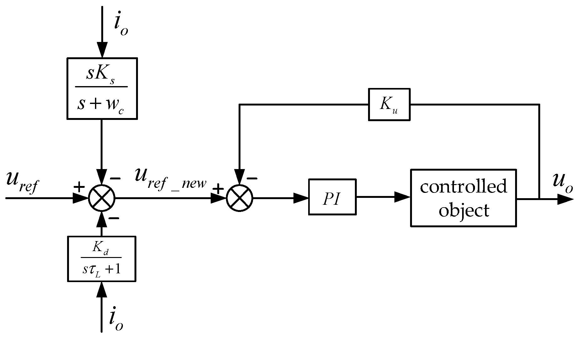
4. Improved Virtual Impedance Droop Control and Stability

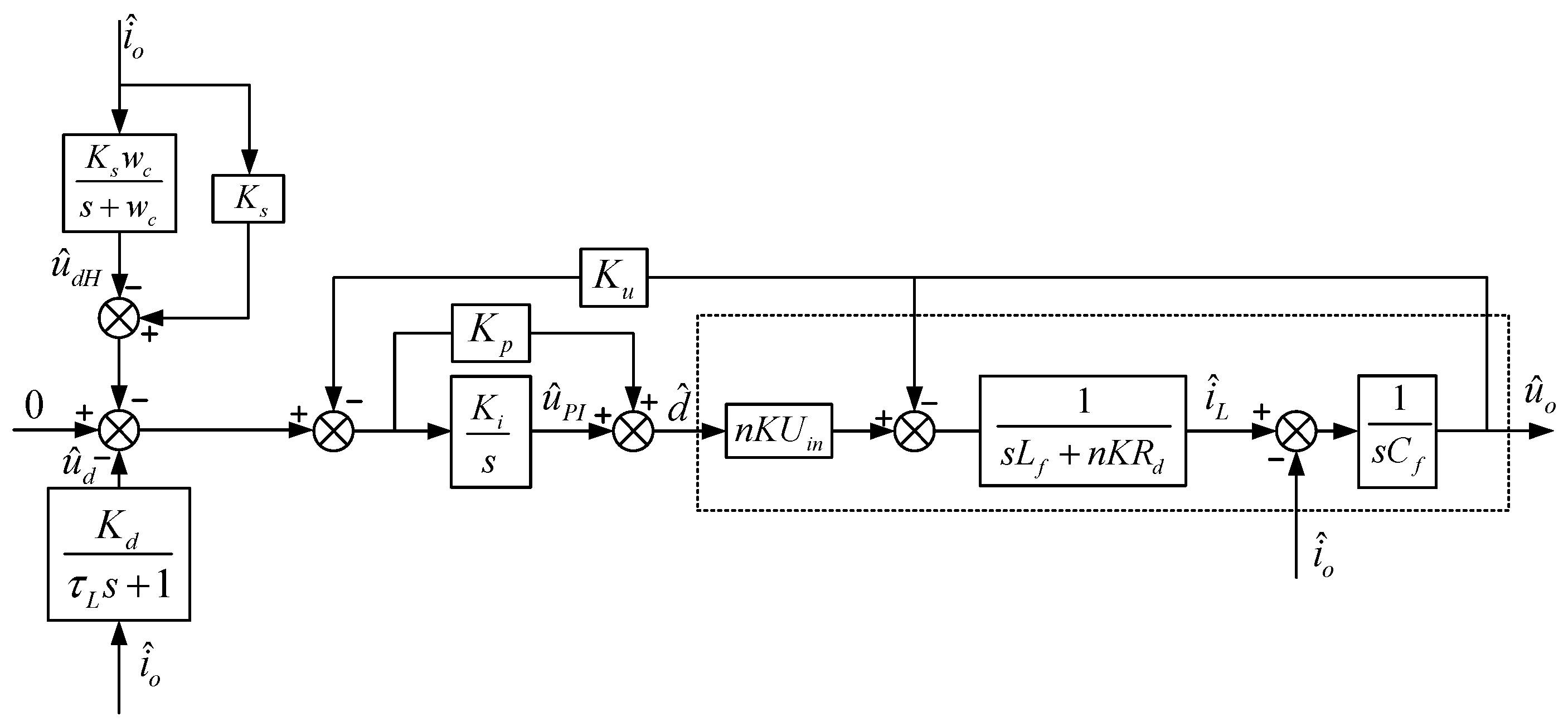
4.1. Improved Virtual Impedance Droop Control

Based on the above analysis, when a large load step is applied to the converter system, the transient response of the output currents of the two converters differs significantly, leading to a severe current imbalance. To suppress the rapid increase in the output current during the transient process of load variation and reduce the dynamic output difference between the parallel converters, an improved virtual impedance droop control strategy is proposed to balance the current imbalance during the transient process.
This strategy introduces a differential controller in the droop control loop, applying negative feedback to the rate of change in the output current. When the rate of change of the output current for a converter is positive and large, the reference output voltage of that converter will decrease due to the positive rate of change, thereby limiting the increase in the duty cycle. Conversely, a converter with a negative rate of change in the output current will increase the reference voltage for the voltage loop control, thereby promoting an increase in its duty cycle. This control strategy effectively improves the current balance during the transient process when load variation occurs, preventing any converter from entering protection mode due to an overcurrent, and it helps the transient currents of each module to balance. To avoid high-frequency noise affecting the control system during steady-state operations, the differential channel output signal is passed through a low-pass filter. The combined effect of this structure essentially forms a high-pass filter, which contributes to improving the current balance in the transient process of the system.
The control block diagram of the improved virtual impedance droop control is as follows:
The given voltage, after passing through both the improved droop and traditional droop control, generates a new reference voltage command, simultaneously addressing both the steady-state operation and transient current sharing during the transient process. During the steady-state operation, the transient droop control has no effect, and the transient droop control value is approximately zero. In this case, the traditional droop control is used to achieve steady-state current sharing. However, during the transient process caused by load changes, as the output current contains strong high-frequency components with large magnitudes, the transient droop control plays a dominant role. This, in turn, adjusts the reference voltage of each converter’s voltage loop, enabling rapid current sharing during the transient process. Compared to the droop control in Figure 3, the improved control strategy incorporates the rate of change in the current into the control during the transient process of load variations, thereby improving current balancing during the transient process.
To facilitate the selection of state variables, the high-pass filter expression in Figure 6 can be rewritten as follows:
G H P F = s K s s + ω c = K s K s ω c s + ω c
To establish a state–space model for the improved virtual impedance droop control, a small-signal block diagram of the improved virtual impedance droop control for the parallel IPOS phase-shift full-bridge converter is shown in Figure 7.
From Figure 7, the following can be derived:
s u ^ d H 1 = K s ω c i ^ o 1 ω c u ^ d H 1
s u ^ d H 2 = K s ω c i ^ o 2 ω c u ^ d H 2
s u ^ P I 1 = K i u ^ d H 1 K i u ^ d 1 K i K u 1 u ^ o K s K i i ^ o 1
s u ^ P I 2 = K i u ^ d H 2 K i u ^ d 2 K i K u 2 u ^ o K s K i i ^ o 2
s i ^ L 1 = n K U i n u ^ P I 1 + n K U i n K p ( u ^ d H 1 u ^ d 1 K u 1 u ^ o K s i ^ o 1 ) u ^ o L f + n K R d
s i ^ L 2 = n K U i n u ^ P I 2 + n K U i n K p ( u ^ d H 2 u ^ d 2 K u 2 u ^ o K s i ^ o 2 ) u ^ o L f + n K R d
Substituting Equations (24) and (25) into the above Equation yields the following:
s u ^ d H 1 = K s ω c ( C f C f 1 C f i ^ L 1 C f 1 C f i ^ L 2 + C f 1 R C f u ^ o u o C f 1 R 2 C f R ^ ) ω c u ^ d H 1
s u ^ d H 2 = K s ω c ( C f 2 C f i ^ L 1 + C f C f 2 C f i ^ L 2 + C f 2 R C f u ^ o u o C f 2 R 2 C f R ^ ) ω c u ^ d H 2
s u ^ P I 1 = K s K i ( C f C f 1 C f i ^ L 1 C f 1 C f i ^ L 2 + C f 1 R C f u ^ o u o C f 1 R 2 C f R ^ ) + K i u ^ d H 1 K i u ^ d 1 K i K u 1 u ^ o
s u ^ P I 2 = K s K i ( C f 2 C f i ^ L 1 + C f C f 2 C f i ^ L 2 + C f 2 R C f u ^ o u o C f 2 R 2 C f R ^ ) + K i u ^ d H 2 K i u ^ d 2 K i K u 2 u ^ o
s i ^ L 1 = n K U i n u ^ P I 1 + n K U i n K P u ^ d H 1 K s ( C f C f 1 C f i ^ L 1 C f 1 C f i ^ L 2 + C f 1 R C f u ^ o u o C f 1 R 2 C f R ^ ) u ^ d 1 K u 1 u ^ o n K R d i ^ L 1 u ^ o L f
s i ^ L 2 = n K U i n u ^ P I 2 + n K U i n K P u ^ d H 2 K s ( C f 2 C f i ^ L 1 + C f C f 2 C f i ^ L 2 + C f 2 R C f u ^ o u o C f 2 R 2 C f R ^ ) u ^ d 2 K u 2 u ^ o n K R d i ^ L 2 u ^ o L f
Similar to the establishment of the IPOS phase-shift full-bridge parallel system model, to establish a state–space model of the parallel system with improved virtual impedance droop control, the state variables are selected as follows: x P = [ i ^ L 1   i ^ L 2   u ^ P I 1   u ^ P I 2   u ^ d 1   u ^ d 2   u ^ d H 1   u ^ d H 2   u ^ o   ] T . The input variable is the disturbance of the load resistance, namely, u = [ R ^ ] . The output variables are the output voltage, the output currents of each converter, and the total output current, namely, y P = [ u ^ o   i ^ o 1   i ^ o 2   i ^ o ] T .
From the above derivation, the state–space model of the improved droop control parallel system can be expressed as follows: x P · = A P x P + B P u , y P = C p x P + D p u , where the system matrix A P , control matrix B P , output matrix C P , and direct transfer matrix   D P are given as follows:
A P = n K R d L f n K U i n K P K s ( C f C f 1 ) L f C f n K U i n K p K s C f 1 L f C f n K U i n L f 0 n K U i n K p L f 0 n K U i n K p L f 0 1 L f n K U i n K p K u 1 L f n K U i n K p K s C f 1 R L f C f n K U i n K p K s C f 2 L f C f n K R d L f n K U i n K P K s ( C f C f 2 ) L f C f 0 n K U i n L f 0 n K U i n K p L f 0 n K U i n K p L f 1 L f n K U i n K p K u 2 L f n K U i n K p K s C f 2 R L f C f K i K s ( C f C f 1 ) C f K i K s C f 1 C f 0 0 K i 0 K i 0 K i K u 1 K i K s C f 1 R C f K i K s C f 2 C f K i K s ( C f C f 2 ) C f 0 0 0 K i 0 K i K i K u 2 K i K s C f 2 R C f K d ( C f C f 1 ) τ L C f K d C f 1 τ L C f 0 0 1 τ L 0 0 0 K d C f 1 τ L R C f K d C f 2 τ L C f K d ( C f C f 2 ) τ L C f 0 0 0 1 τ L 0 0 K d C f 2 τ L R C f K s w c ( C f C f 1 ) C f K s w c C f 1 C f 0 0 0 0 w c 0 K s w c C f 1 R C f K s w c C f 2 C f K s w c ( C f C f 2 ) C f 0 0 0 0 0 w c K s w c C f 2 R C f 1 C f 1 C f 0 0 0 0 0 0 1 R C f
B P = n K U i n K p K s u o C f 1 R 2 C f n K U i n K p K s u o C f 2 R 2 C f K i K s C f 1 R 2 C f K i K s C f 2 R 2 C f K d u o C f 1 τ L R 2 C f K d u o C f 2 τ L R 2 C f K s w c u o C f 1 R 2 C f K s w c u o C f 2 R 2 C f u o R 2
C P = 0 0 0 0 0 0 0 0 1 C f C 1 C f C 1 C f 0 0 0 0 0 0 C f 1 R C f C 2 C f C f C 2 C f 0 0 0 0 0 0 C f 2 R C f 0 0 0 0 0 0 0 0 1 R
D P = 0 u o C f 1 R 2 C f u o C f 2 R 2 C f u o R 2
In the steady state, the system state variables increase only by   u d H 1 and   u d H 2 , and their steady-state values before the step are as follows:
u d H 1 = K s i o 1 = 12 × 1 = 12
u d H 2 = K s i o 2 = 12 × 14 = 168
After the step, their values are u d H 1 = 12 × 13 = 36 and u d H 2 = 12 × 26 = 192 .
Here, K s is selected as 12, and ω c is selected as 8 Hz. At this point, the system’s initial conditions are as follows: x P ( 0 ) = [ 2   2   0.001   0.0045   3   3   24   24   3 ] .
The state–space model of the parallel system with the improved virtual impedance droop control is given by the following: x P · = A P x P + B P u , y P = C P x P + D P u . Similarly, the result can be obtained from Equation (44) as follows:
y P ( s ) = C P ( s I A P ) 1 B P u 0 ( s ) + x P ( 0 ) + D P u 0 ( s )
The step response of the output current for the same input variable step, considering the initial conditions x P ( 0 ) , can be obtained and plotted using MATLAB 2024a, as shown in Figure 8.
As can be clearly seen in Figure 8, the transient current response of the system during load transients shows a significant improvement after the introduction of the improved virtual impedance. The magnitude of the current imbalance is significantly reduced, and the tendency for current overshoot in the converter with a smaller feedback coefficient during the transient process is effectively suppressed. Furthermore, the time required for the system to achieve current sharing is shortened, indicating that the speed of dynamic current balancing is effectively enhanced. This demonstrates that the improved virtual impedance control strategy can effectively mitigate the current imbalance during transient processes.

4.2. Improved Virtual Impedance Control Stability Analysis

Based on the state–space model with the improved droop control, the eigenvalues of the state matrix   A P are calculated. The system stability after the introduction of the improved control strategy is analyzed by examining the location of the eigenvalues [51]. Due to the poor stability of the phase-shift full-bridge parallel system under light-load conditions, an analysis is conducted under light-load conditions to determine whether the system is stable. A stability analysis was conducted under a 5 kW load condition, with the other system parameters shown in Table 1. The analysis is carried out from two aspects: the high-pass filter gain K s and the cutoff frequency ω c .

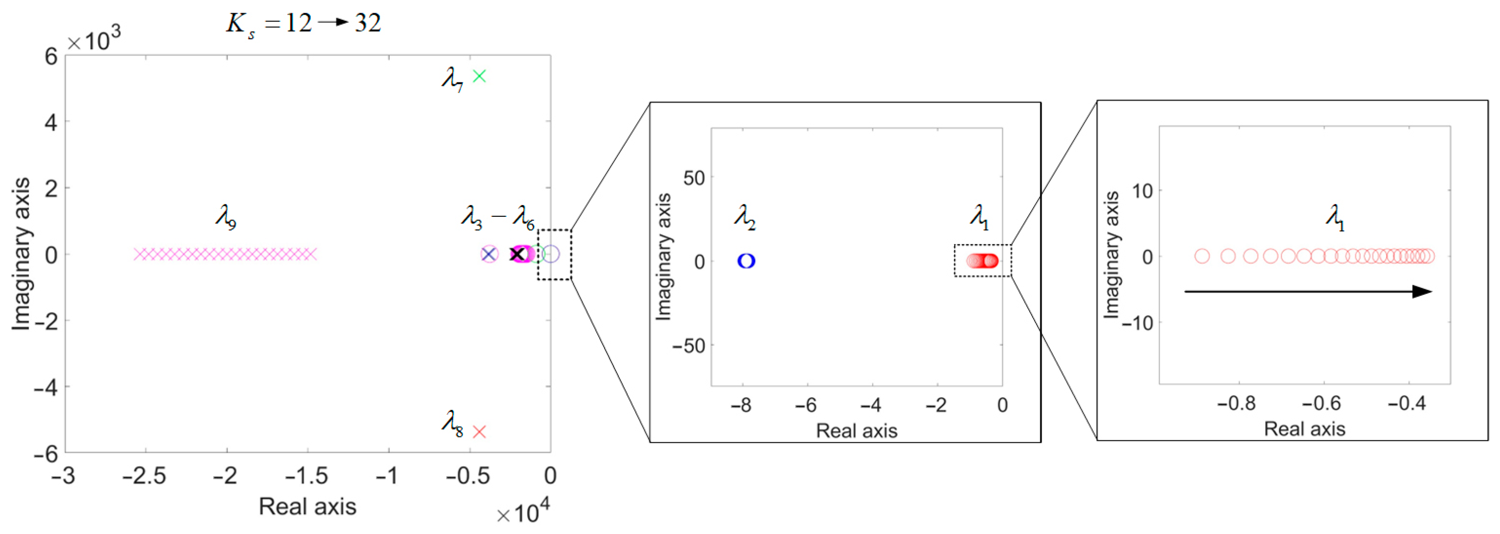
4.2.1. Impact of Gain on System Stability and Dynamic Performance

Under the condition of a fixed cutoff frequency for the high-pass filter, the trajectory of the characteristic roots of the parallel system as the high-pass filter gain increases from 12 to 32, as shown in Figure 9.
In Figure 9, λ 1 to λ 9 represent the system’s eigenvalues. It can be observed that as the gain K s   gradually increases, the dominant characteristic roots on the real axis move closer to the imaginary axis, resulting in a decrease in system damping and an increase in response time. Due to the introduction of the current rate of change into the control, the reference voltage experiences a noticeable drop during a load disturbance. During the transient process, the voltage undergoes a relatively large dip. The introduction of a negative feedback mechanism achieves transient current balancing. No right-half plane poles appear, and the system remains stable.

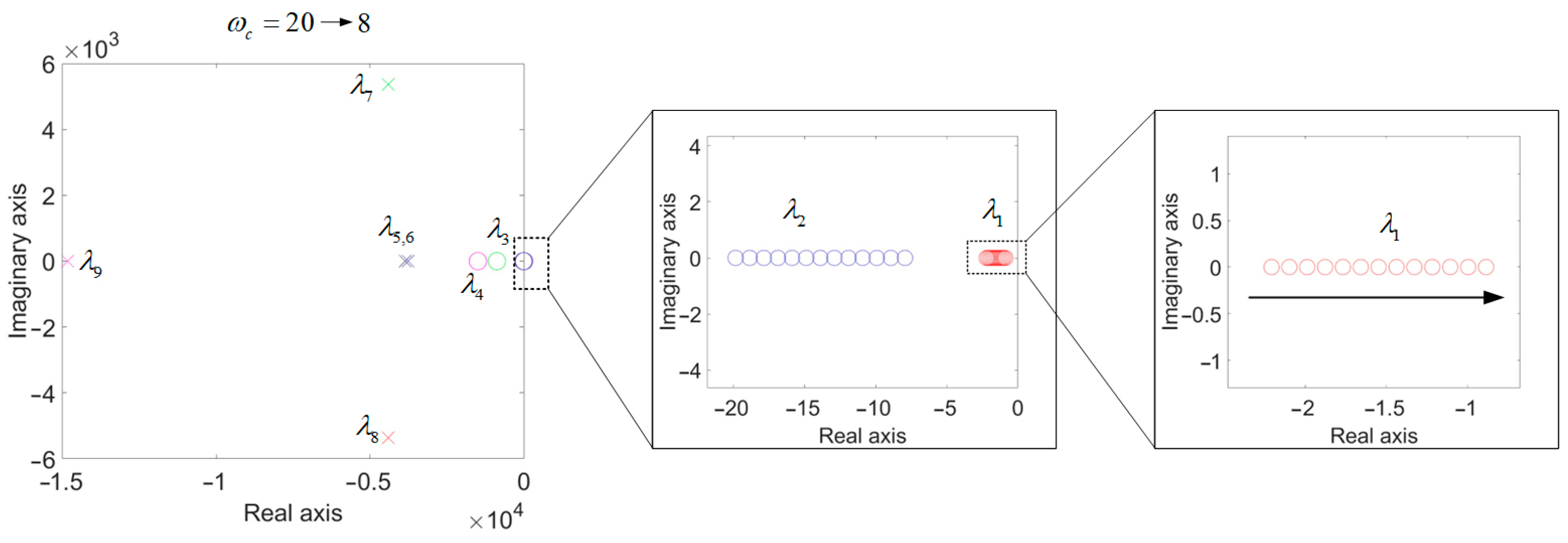
4.2.2. Impact of Cutoff Frequency on System Stability and Dynamic Performance

When the high-pass filter gain is kept constant and its cutoff frequency is gradually reduced from 20 Hz to 8 Hz, the variation in the characteristic root trajectory is as shown in Figure 10.
In Figure 10, λ 1 to λ 9 represent the system’s eigenvalues. It can be seen that, as the cutoff frequency gradually decreases, the main poles on the real axis move closer to the imaginary axis, which results in a slower system response. However, throughout this change, no poles in the right-half plane appear, and the system remains stable.
From the above analysis, it can be seen that the improved virtual impedance droop control strategy keeps the system stable even under light-load conditions. By appropriately selecting the high-pass filter gain and cutoff frequency parameters, the dynamic balance during the transient process can be improved.

5. Simulation and Experimental Verification
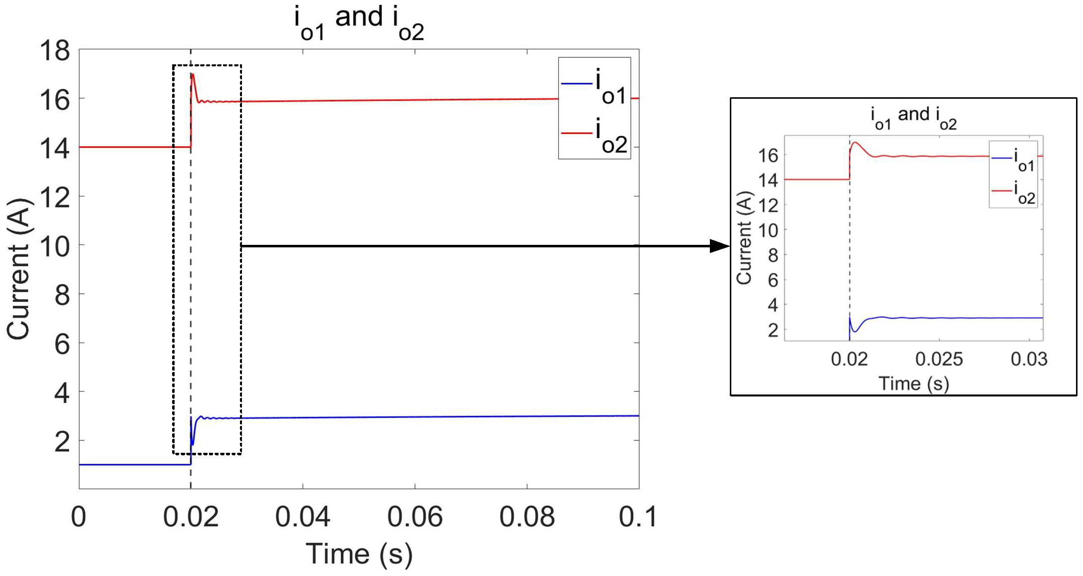
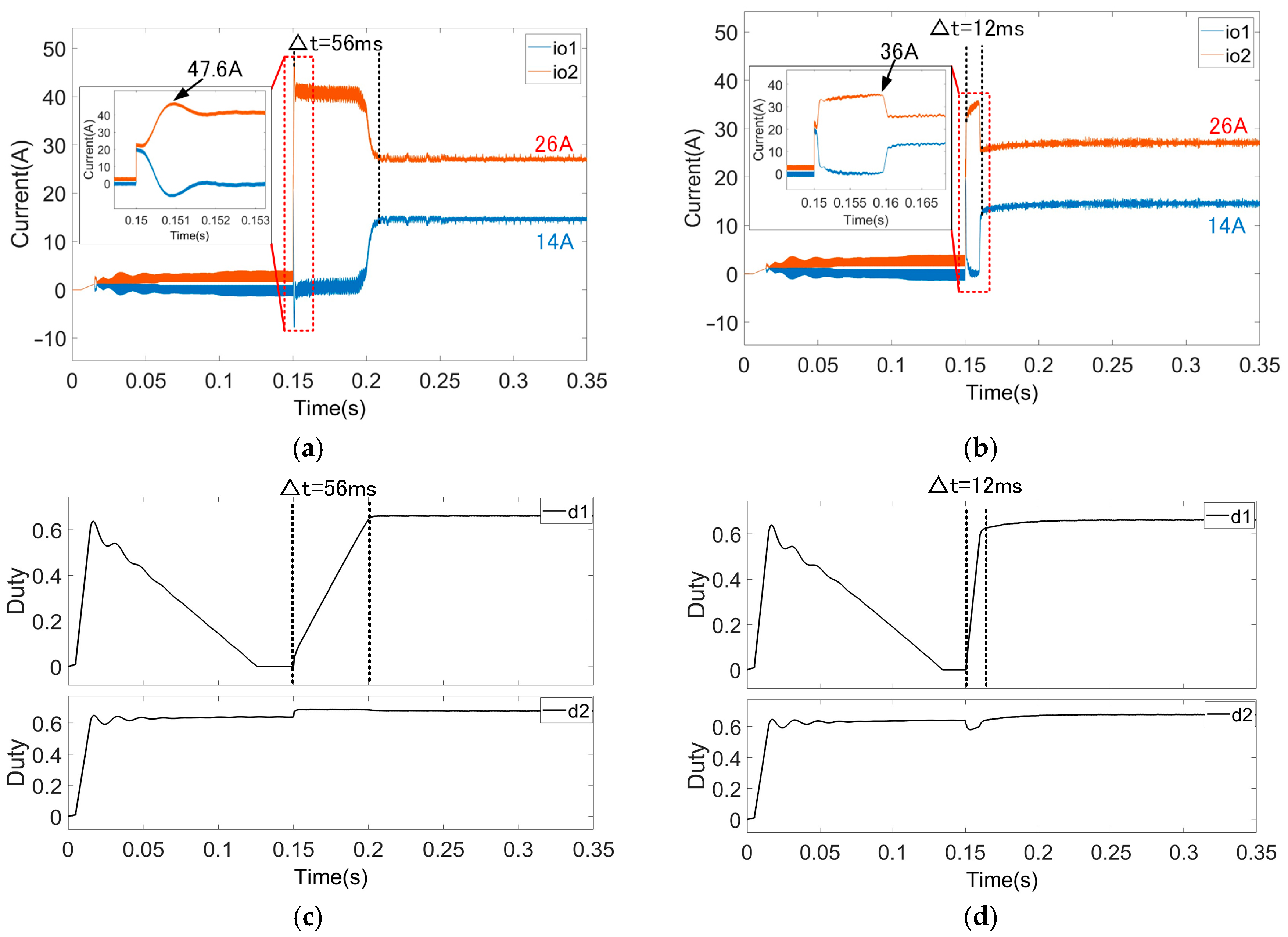
5.1. Simulation

Using MATLAB/Simulink 2024a simulation software, a parallel system of two IPOS phase-shift full-bridge converters was constructed based on the parameters listed in Table 1 to observe the output current during a load step increase. Initially, without the improved control strategy, a load step was applied to the parallel system. At 0.15 s, the load power increased from 5 kW to 80 kW, and the simulation results are shown in Figure 11a,c. After implementing the improved control strategy, the same load step was applied under identical conditions. At 0.15 s, the load power increased from 5 kW to 80 kW, and the simulation results are shown in Figure 11b,d.
In Figure 11, i o 1 is the output current of Converter 1, i o 2 is the output current of Converter 2, d 1 is the duty cycle of Converter 1, and d 2 is the duty cycle of Converter 2.
In Figure 11a, it can be observed that, during the load step increase, the converter with the smaller output voltage feedback coefficient, Converter 2, exhibits a higher transient peak current, with an overshoot of 83.07%. After approximately 56 ms, the other converter, Converter 1, begins to share the load. Before current sharing is re-established, the entire load is handled by Converter 2, resulting in a longer time to achieve current sharing. Figure 11c shows the duty cycle waveforms of the two converters. Under light-load conditions, the duty cycle of Converter 1, which has a larger output voltage feedback coefficient, reduces to zero, while Converter 2, with a smaller feedback coefficient, maintains a normal steady-state duty cycle. After introducing the improved control strategy, the output current waveforms of the two converters are as shown in Figure 11b. In this case, the overshoot of Converter 2’s output current is reduced to 38.46%, which is significantly lower than the case without the improved virtual impedance. Converter 1 begins to share the load at approximately 12 ms. By comparing Figure 11c,d, it can be observed that, after introducing the improved control, the rise rate of Converter 1’s duty cycle increases, and the rise time is shortened. This allows for faster voltage output, achieving more optimal transient current sharing performance.

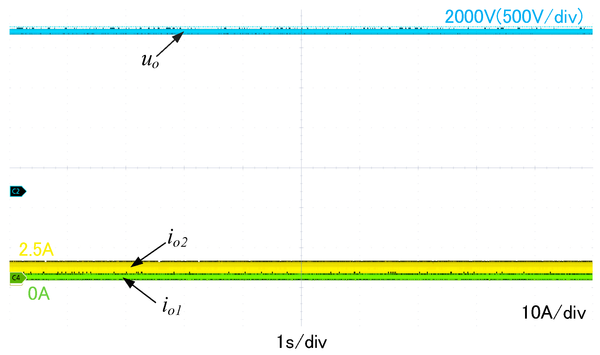
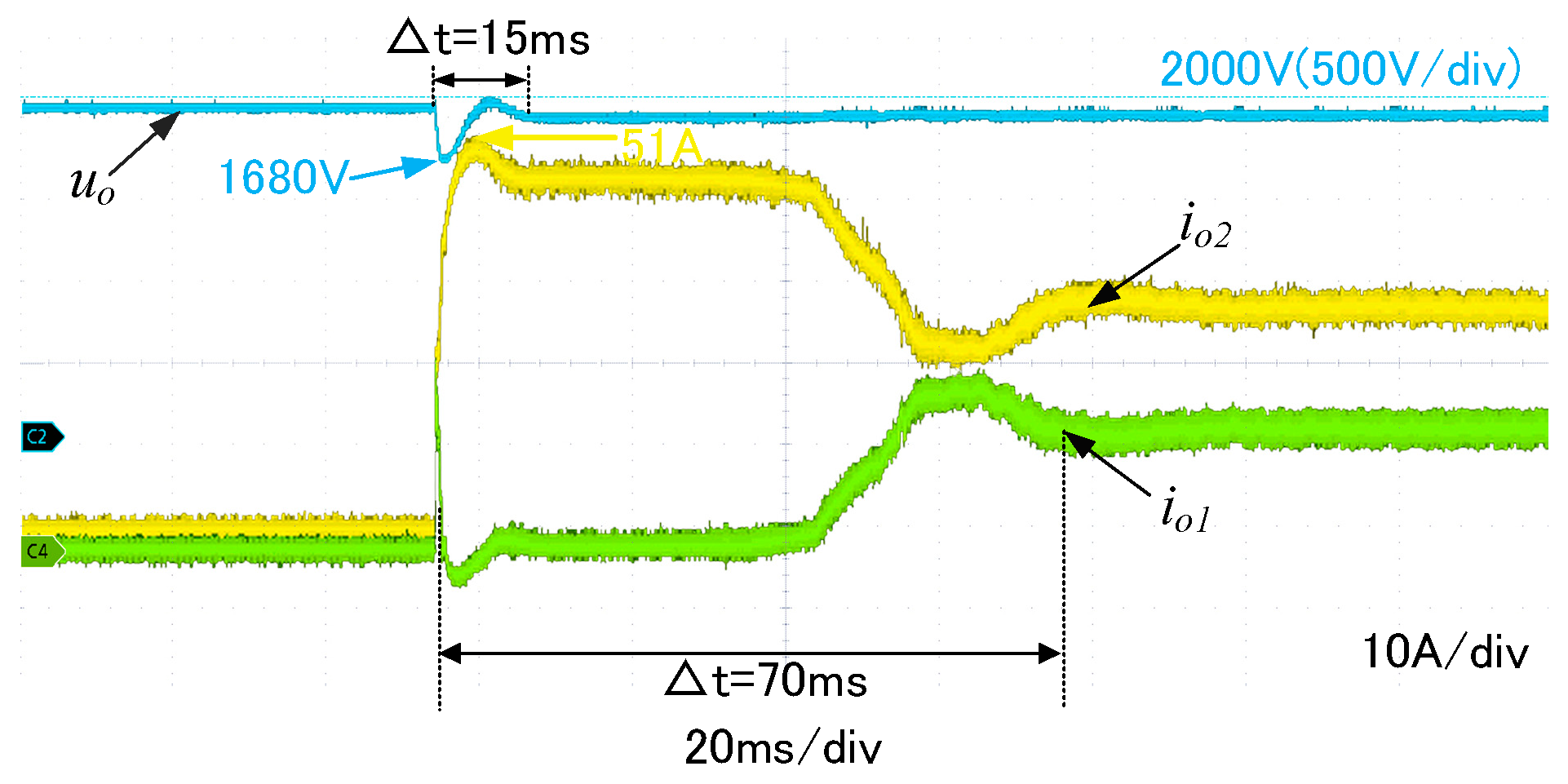
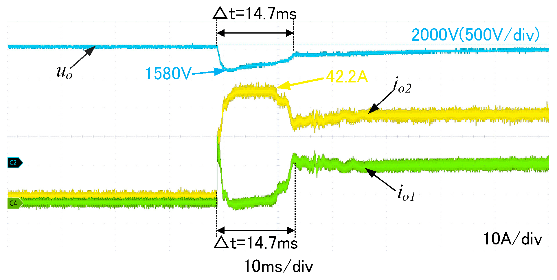
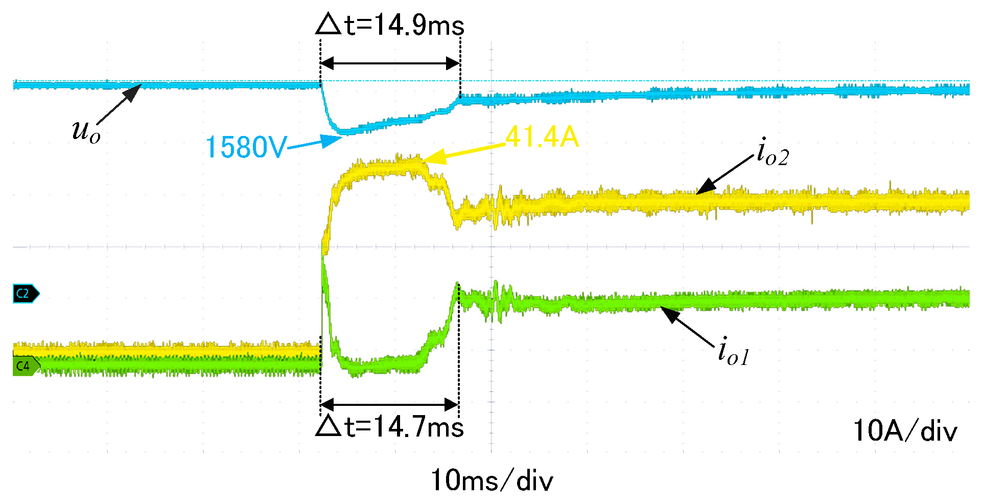
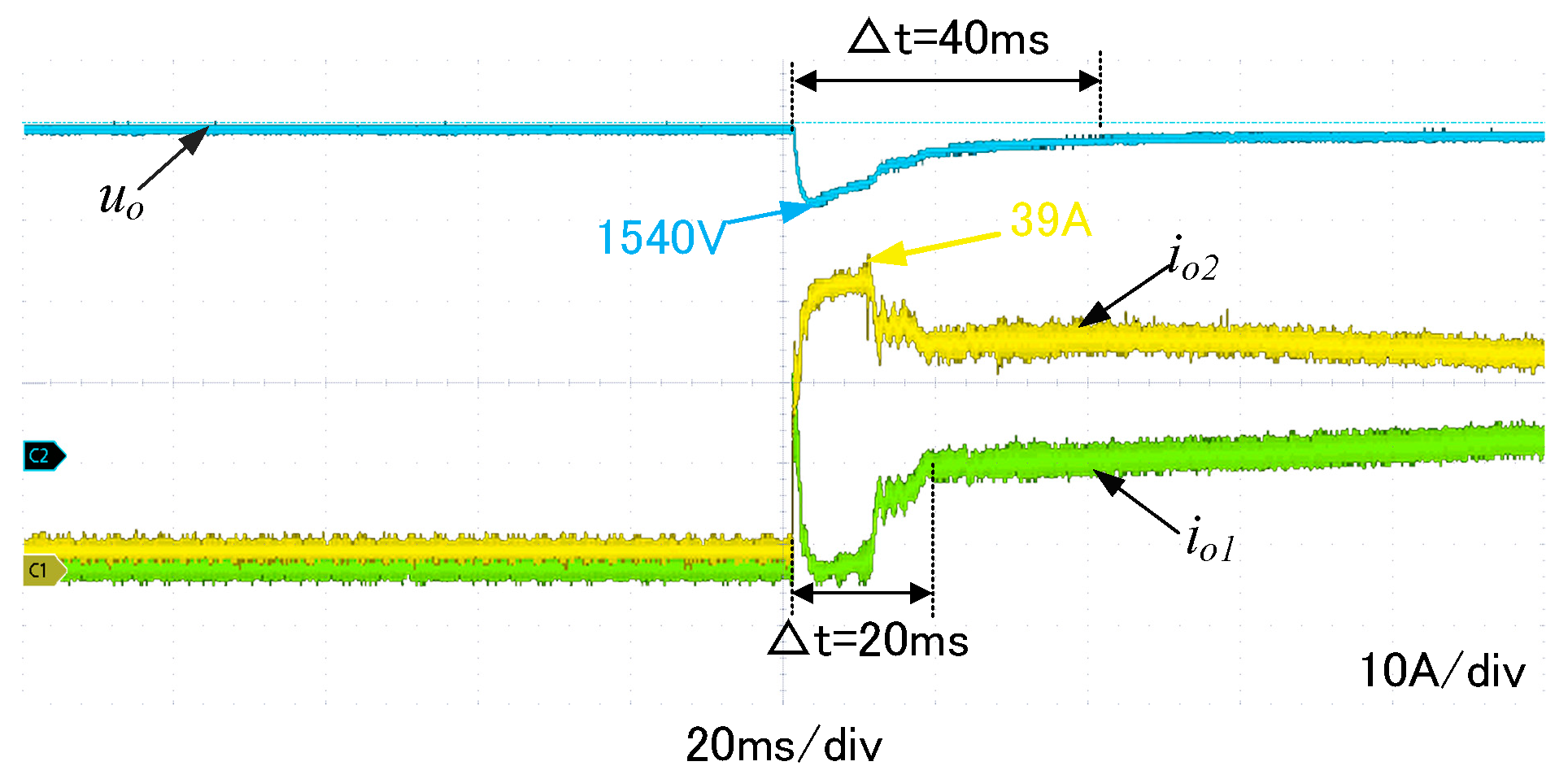
5.2. Experimental Verification

The correctness of the influence of the output voltage feedback coefficient on the current sharing process of the parallel system consisting of two 100 kW IPOS phase-shift full-bridge prototypes is verified, and the effectiveness of the proposed improved control strategy is validated. The parameters of the prototypes are shown in Table 1. Figure 12 shows the test stand of the parallel system.
Figure 13 shows the output current and output voltage waveforms of the two parallel converters when they reach a stable output under light-load conditions. In the figure, it can be observed that, at a steady-state output voltage, the output currents of the two converters are not the same. One converter outputs 0 A, while the other converter outputs 2.5 A at 5 kW, which is consistent with the theoretical analysis. Figure 14 shows the output current and output voltage waveforms under a sudden load increase to 80 kW, without the improved control strategy. In the figure, it can be clearly observed that the dynamic behavior of the two converters is completely opposite. One converter’s current peak reaches 51 A, while the other converter’s output current drops to 0. The time to achieve current sharing again is approximately 70 ms. The output voltage drops to a minimum of 1680 V, and the voltage recovery time is about 15 ms. When a steady state is reached, the output currents of Converters 1 and 2 are 14.6 A and 25.4 A, respectively. The overshoot of Converter 2 is 100.7%.
In the figure, u o represents the output voltage of the parallel system, i o 1 is the output current of Converter 1, and i o is the output current of Converter 2.
Figure 15 shows the output waveforms under a load step change after the improved control strategy is implemented. The parameters include a high-pass filter gain of 8 and a cutoff frequency of 15 Hz. At a steady state, the output is the same as before the improvement, with a current peak of 42.2 A, which is 6 A lower than before the improved control strategy was applied. The overshoot is 66%, and the time for both converters to reach current sharing again is approximately 14.7 ms. The output voltage drops to a minimum of 1580 V, and the voltage recovery time is about 15 ms. Figure 16 shows the output waveforms with a high-pass filter gain of 8 and a cutoff frequency of 12 Hz. After the load step increase, the voltage drops to a minimum of 1580 V, the current peak is 41.4 A, the overshoot is 62.9%, and the voltage recovery time is about 14.9 ms. The time to achieve current sharing again is approximately 14.7 ms. Figure 17 shows the output waveforms with a high-pass filter gain of 10 and a cutoff frequency of 12 Hz. The current peak is 39.8 A, the overshoot is 53.5%, and the time to reach current sharing again is about 20 ms. The output voltage drops to a minimum of 1540 V, and the voltage recovery time is 40 ms.
It can be seen that, as the gain increases or the cutoff frequency decreases, the effect of suppressing the current peak becomes more effective. The overshoot of the output current significantly decreases, but this also results in a larger voltage drop.
In summary, the improved virtual impedance droop control strategy can significantly reduce the current peak during load step increases and improve the system’s transient current sharing performance. However, it is necessary to find a reasonable balance between the gain and cutoff frequency in order to achieve optimal dynamic performance, balancing the suppression of current peaks and the reduction in voltage drops.

6. Conclusions

In parallel systems, due to the difficulty in ensuring complete uniformity between each converter, there is usually a certain degree of dispersion among the module parameters. Among these, differences in the voltage loop output voltage feedback coefficients significantly affect the system’s transient current sharing and dynamic performance. Typically, current sharing methods cannot guarantee current balance during transient processes. This study analyzes the impact mechanism of the output voltage feedback coefficient on transient current imbalance and proposes an improved virtual impedance control strategy. This strategy effectively mitigates the current imbalance induced by load step changes, thereby significantly enhancing the system’s transient current sharing capability. In the proposed approach, an improved virtual impedance is introduced and applied via a negative feedback mechanism to alleviate the transient current imbalance in parallel converters. Importantly, because the strategy only targets the transient process and does not alter the converter’s inherent characteristics, it does not affect the steady-state current sharing. As a result, the proposed method is suitable for a wide range of DC/DC topologies and offers valuable guidance for practical engineering applications.

Author Contributions

Conceptualization, M.F. and H.C.; methodology, M.F. and X.L.; formal analysis, H.C. and X.L.; investigation, X.L.; resources, H.C. and X.L.; data curation, X.L.; writing—original draft preparation, M.F.; writing—review and editing, H.C. and X.L.; funding acquisition, H.C. All authors have read and agreed to the published version of the manuscript.

Funding

This research was funded by the Innovation Fund for Industry–Academia–Research Collaboration of Chinese Higher Education Institutions (2024HY031).

Data Availability Statement

The data presented in this study are available on request from the corresponding author.

Conflicts of Interest

The authors declare no conflicts of interest.

References

  1. Zhang, L.; Tu, C.; Xiao, F.; Liu, B.; Li, P. Intrinsic Regularity Analysis and Optimization Control of Current Stress and RMS for Dual-Active Bridge Converter. Electronics 2024, 13, 4802. [Google Scholar] [CrossRef]
  2. Darwish, A. A Modular Step-Up DC/DC Converter for Electric Vehicles. Energies 2024, 17, 6305. [Google Scholar] [CrossRef]
  3. Ren, C.; He, Y.; Qin, Y.; Hui, Y.; Li, X.; Han, X.; He, X. A Novel Modular Sigma DC/DC Converter with a Wide Input Voltage Range. Electronics 2024, 13, 995. [Google Scholar] [CrossRef]
  4. Kroičs, K.; Gaspersons, K.; Elkhateb, A. Response Time Reduction of DC–DC Converter in Voltage Mode with Application of GaN Transistors and Digital Control. Electronics 2024, 13, 901. [Google Scholar] [CrossRef]
  5. Kok, C.L.; Tang, H.; Teo, T.H.; Koh, Y.Y. A DC-DC Converter with Switched-Capacitor Delay Deadtime Controller and Enhanced Unbalanced-Input Pair Zero-Current Detector to Boost Power Efficiency. Electronics 2024, 13, 1237. [Google Scholar] [CrossRef]
  6. Shinde, N.; Sankad, S.; Patil, S.L. Design and Study Voltage Characteristics of Buck Converter by Matlab Simulink. In Proceedings of the 2018 2nd International Conference on Trends in Electronics and Informatics (ICOEI), Tirunelveli, India, 11–12 May 2018; pp. 680–683. [Google Scholar]
  7. Reyes-Malanche, J.A.; Vázquez, N.; Leyva-Ramos, J. Switched-capacitor quadratic buck converter for wider conversion ratios. IET Power Electron. 2015, 8, 2370–2376. [Google Scholar] [CrossRef]
  8. Fan, S.; Sun, L.; Duan, J.; Zhang, K. Improved active clamped ZVS buck converter with freewheeling current transfer circuit. IET Power Electron. 2019, 12, 1341–1348. [Google Scholar] [CrossRef]
  9. Botao, Z.; Qi, W.; Min, Z.; Huan, H. Analytical solution for the inductor current of BOOST converter. IET Power Electron. 2019, 12, 2424–2432. [Google Scholar] [CrossRef]
  10. Muhammad, M.; Armstrong, M.; Elgendy, M.A. A Nonisolated Interleaved Boost Converter for High-Voltage Gain Applications. IEEE J. Emerg. Sel. Top. Power Electron. 2015, 4, 352–362. [Google Scholar] [CrossRef]
  11. Atmaca, Ö.; Erol, E.; Kamal, T.; Karabacak, M. Design of an H-Bridge Bidirectional DC-DC Converter with LCL Filter for High Power Battery Applications. In Proceedings of the 2019 1st Global Power, Energy and Communication Conference (GPECOM), Nevsehir, Turkey, 12–15 June 2019; pp. 238–241. [Google Scholar]
  12. Gummi, K.; Ferdowsi, M. Derivation of new double-input DC-DC converters using H-Bridge cells as building blocks. In Proceedings of the 2008 34th Annual Conference of IEEE Industrial Electronics, Orlando, FL, USA, 10–13 November 2008; pp. 2806–2811. [Google Scholar]
  13. Lazar, J.F.; Martinelli, R. Steady-state analysis of the LLC series resonant converter. In Proceedings of the APEC 2001. Sixteenth Annual IEEE Applied Power Electronics Conference and Exposition (Cat. No. 01CH37181), Anaheim, CA, USA, 4–8 March 2001. [Google Scholar]
  14. Tang, W.; Wang, H.; Zhu, X.; Gao, W.; Zheng, Z.; Yue, X. A Passive Current Sharing Method for Two-Phase Common Inductor LLC Resonant Converters and Mathematical Analysis of Current Sharing Effect. IEEE Trans. Power Electron. 2022, 37, 12316–12326. [Google Scholar] [CrossRef]
  15. Lee, J.-Y.; Jeong, Y.-S.; Han, B. An Isolated DC/DC Converter Using High-Frequency Unregulated Resonant Converter for Fuel Cell Applications. IEEE Trans. Ind. Electron. 2011, 58, 2926–2934. [Google Scholar] [CrossRef]
  16. García Pérez, R.A.; Muñoz-Cruzado-Alba, J.; Galván Díez, E.; Carrasco Solís, J.M. Classification of Design Methodologies of Dual Active Bridge-Based Resonant Converters for Battery Energy Storage Systems. Electronics 2024, 13, 4748. [Google Scholar] [CrossRef]
  17. Jia, D.; Wang, D. Current Stress Minimization Based on Particle Swarm Optimization for Dual Active Bridge DC–DC Converter. Actuators 2024, 13, 421. [Google Scholar] [CrossRef]
  18. Kang, Z.; Li, L.; Zhang, H. Feedforward Control Strategy of a DC-DC Converter for an Off-Grid Hydrogen Production System Based on a Linear Extended State Observer and Super-Twisting Sliding Mode Control. Electronics 2024, 13, 3934. [Google Scholar] [CrossRef]
  19. Zhang, Y.; Guo, X.; Guo, B.; Bian, Y. The simulation and design of PSFB ZVS DC-DC converter based on Saber. In Proceedings of the 2014 IEEE Conference and Expo Transportation Electrification Asia-Pacific (ITEC Asia-Pacific), Beijing, China, 31 August–3 September 2014; pp. 1–4. [Google Scholar]
  20. Benites Quispe, J.B.; Mezaroba, M.; Batschauer, A.L.; de Souza Ribeiro, J.M. A Reconfigurable Phase-Shifted Full-Bridge DC–DC Converter with Wide Range Output Voltage. Energies 2024, 17, 3483. [Google Scholar] [CrossRef]
  21. Liu, J.; Gong, C.; Zhang, Y. A Novel Second Harmonic Voltage Suppression Control for PSFB Converter in Dual-Stage Single-Phase Rectifier. Electronics 2024, 13, 1830. [Google Scholar] [CrossRef]
  22. Wang, H.; Yang, G.; Kang, W.; Zhang, X.; Fan, X.; Xiao, F. Minimum-Output-Current-Ripple Control of Current-Fed Three-Level Phase-Shift Full-Bridge Converter. Energies 2022, 15, 6444. [Google Scholar] [CrossRef]
  23. Sun, X.; Zhou, Y.; Chen, G.; Ren, B. Model Predictive Control of a Phase-Shifted Full-Bridge DC-DC Converter. In Proceedings of the 2020 IEEE 9th International Power Electronics and Motion Control Conference (IPEMC2020-ECCE Asia), Nanjing, China, 29 November–2 December 2020; pp. 2710–2714. [Google Scholar]
  24. Bakan, A.F.; Altintaş, N.; Aksoy, İ. An Improved PSFB PWM DC–DC Converter for High-Power and Frequency Applications. IEEE Trans. Power Electron. 2013, 28, 64–74. [Google Scholar] [CrossRef]
  25. Wang, J.B. Parallel DC/DC converters system with a novel primary droop current sharing control. IET Power Electron. 2012, 5, 1569–1576. [Google Scholar] [CrossRef]
  26. Jin, Z.; Savaghebi, M.; Vasquez, J.C.; Meng, L.; Guerrero, J.M. Maritime DC microgrids–a combination of microgrid technologies and maritime onboard power system for future ships. In Proceedings of the 2016 IEEE 8th International Power Electronics and Motion Control Conference (IPEMC-ECCE Asia), Hefei, China, 22–26 May 2016; pp. 179–184. [Google Scholar]
  27. Liu, W.-S.; Chen, J.-F.; Liang, T.-J.; Lai, T.-L. Implementation and design of hybrid power module for DC power grid in paralleled applications. In Proceedings of the 2013 IEEE 10th International Conference on Power Electronics and Drive Systems (PEDS), Kitakyushu, Japan, 22–25 April 2013; pp. 323–329. [Google Scholar]
  28. Liu, J.; Gong, C.; Zhang, Y. Global Efficiency Optimal Control Strategy for Parallel Phase Shift Full-bridge Converter. In Proceedings of the 2023 IEEE International Conference on Predictive Control of Electrical Drives and Power Electronics (PRECEDE), Wuhan, China, 16–19 June 2023; pp. 1–6. [Google Scholar]
  29. Shi, J.; Zhou, L.; He, X. Common-Duty-Ratio Control of Input-Parallel Output-Parallel (IPOP) Connected DC–DC Converter Modules With Automatic Sharing of Currents. IEEE Trans. Power Electron. 2012, 27, 3277–3291. [Google Scholar] [CrossRef]
  30. Panov, Y.; Rajagopalan, J.; Lee, F.C. Analysis and design of N paralleled DC-DC converters with master-slave current-sharing control. In Proceedings of the APEC 97–Applied Power Electronics Conference, Atlanta, GA, USA, 23–27 February 1997; Volume 1, pp. 436–442. [Google Scholar]
  31. Ghanbari, N.; Bhattacharya, S. Adaptive Droop Control Method for Suppressing Circulating Currents in DC Microgrids. IEEE Open Access J. Power Energy 2020, 7, 100–110. [Google Scholar] [CrossRef]
  32. Li, C.; Wu, J.; Zhang, K.; Dai, X.; Xu, S. Improved droop control based voltage compensation and variable droop coefficient in DC microgrids. In Proceedings of the 2016 UKACC 11th International Conference on Control (CONTROL), Belfast, UK, 31 August–2 September 2016; pp. 1–6. [Google Scholar]
  33. Cousineau, M.; Xiao, Z. Fully decentralized modular approach for parallel converter control. In Proceedings of the 2013 28th Annual IEEE Applied Power Electronics Conference and Exposition (APEC), Long Beach, CA, USA, 17–21 March 2013; pp. 237–243. [Google Scholar]
  34. Hernandez, B.; Giraldo, E.; Ospina, S.; Garces, A. Master-Slave Operation of DC Microgrids: An Adaptive Control Approach with Estimation. In Proceedings of the 2019 IEEE 4th Colombian Conference on Automatic Control (CCAC), Medellin, Colombia, 15–18 October 2019; pp. 1–6. [Google Scholar]
  35. Anand, S.; Fernandes, B.G.; Guerrero, J. Distributed Control to Ensure Proportional Load Sharing and Improve Voltage Regulation in Low-Voltage DC Microgrids. IEEE Trans. Power Electron. 2013, 28, 1900–1913. [Google Scholar] [CrossRef]
  36. Vivek, K. Design and Analysis of Voltage Droop Control Technique for DC Microgrids. In Proceedings of the 2019 3rd International Conference on Electronics, Communication and Aerospace Technology (ICECA), Coimbatore, India, 12–14 June 2019; pp. 795–799. [Google Scholar]
  37. Hassan, M.A.; Li, E.; Chi, S.; Li, T.; Cheng, L.; Duan, C. Sliding Mode Control of Parallel-Connected DC-DC Buck Power Converters in DC Microgrid Systems. In Proceedings of the 2018 IEEE International Power Electronics and Application Conference and Exposition (PEAC), Shenzhen, China, 4–7 November 2018; pp. 1–6. [Google Scholar]
  38. Prabhakaran, P.; Goyal, Y.; Agarwal, V. Novel Nonlinear Droop Control Techniques to Overcome the Load Sharing and Voltage Regulation Issues in DC Microgrid. IEEE Trans. Power Electron. 2018, 33, 4477–4487. [Google Scholar] [CrossRef]
  39. Gong, B.; Liu, K.; Luan, H.; Wu, J.; Zhou, J.; Tan, S.; Huang, C.; Wu, H. Design of a Dynamic Hybrid Compensator for Current Sharing Control of Parallel Phase-Shifted Full-Bridge Converter. Energies 2023, 16, 2204. [Google Scholar] [CrossRef]
  40. You, J.; Cheng, L.; Fu, B.; Deng, M. Analysis and Control of Input-Parallel Output-Series Based Combined DC/DC Converter With Modified Connection in Output Filter Circuit. IEEE Access 2019, 7, 58264–58276. [Google Scholar] [CrossRef]
  41. Qin, Z.; Cai, H.; Lin, X. Stability Analysis and Control Strategy Optimization of a Paralleled IPOS Phase-Shifted Full-Bridge Converters System Based on Droop Control. Electronics 2023, 12, 3685. [Google Scholar] [CrossRef]
  42. Augustine, S.; Mishra, M.K.; Lakshminarasamma, N. Circulating current minimization and current sharing control of parallel boost converters based on Droop Index. In Proceedings of the 2013 9th IEEE International Symposium on Diagnostics for Electric Machines, Power Electronics and Drives (SDEMPED), Valencia, Spain, 27–30 August 2013; pp. 454–460. [Google Scholar]
  43. Dadi, R.; Meenakshy, K.; Damodaran, S.K. A Modified Droop Control Method for DC Microgrid with Improved Voltage Regulation and Current Sharing. In Proceedings of the 2020 International Conference on Power, Instrumentation, Control and Computing (PICC), Thrissur, India, 17–19 December 2020; pp. 1–6. [Google Scholar]
  44. Lin, X.; Zamora, R.; Baguley, C. Droop Control Based on Improved Virtual Impedance in a Stand-Alone Microgrid. In Proceedings of the 2019 IEEE PES GTD Grand International Conference and Exposition Asia (GTD Asia), Bangkok, Thailand, 19–23 March 2019; pp. 883–888. [Google Scholar]
  45. Liu, H.; Chen, Y.; Li, S.; Hou, Y. Improved droop control of isolated microgrid with virtual impedance. In Proceedings of the 2013 IEEE Power & Energy Society General Meeting, Vancouver, BC, Canada, 21–25 July 2013; pp. 1–5. [Google Scholar]
  46. Thomas, V.; Kumaravel, S.; Ashok, S. Control of parallel DC-DC converters in a DC microgrid using virtual output impedance method. In Proceedings of the 2016 2nd International Conference on Advances in Electrical, Electronics, Information, Communication and Bio-Informatics (AEEICB), Chennai, India, 27–28 February 2016; pp. 587–591. [Google Scholar]
  47. Yogithanjali Saimadhuri, K.N.; Janaki, M. Advanced control strategies for microgrids: A review of droop control and virtual impedance techniques. Results Eng. 2025, 25, 103799. [Google Scholar] [CrossRef]
  48. Dorf, R.C.; Bishop, R.H. Modern Control Systems; Pearson: Upper Saddle River, NJ, USA, 2015. [Google Scholar]
  49. Deraz, S.A.; Zaky, M.S.; Tawfiq, K.B.; Mansour, A.S. State Space Average Modeling, Small Signal Analysis, and Control Implementation of an Efficient Single-Switch High-Gain Multicell Boost DC-DC Converter with Low Voltage Stress. Electronics 2024, 13, 3264. [Google Scholar] [CrossRef]
  50. Vlatkovic, V.; Sabate, J.A.; Ridley, R.B.; Lee, F.C.; Cho, B.H. Small-signal analysis of the phase-shifted PWM converter. IEEE Trans. Power Electron. 1992, 7, 128–135. [Google Scholar] [CrossRef]
  51. Lv, Z.; Zhou, M.; Wang, Q.; Hu, W. Small-Signal Stability Analysis for Multi-Terminal LVDC Distribution Network Based on Distributed Secondary Control Strategy. Electronics 2021, 10, 1575. [Google Scholar] [CrossRef]
Figure 1. Diagram of an IPOS phase-shifted full-bridge converter circuit.
Electronics 14 00714 g001
Figure 2. Small-signal mathematical model of the IPOS phase-shift full-bridge system.
Electronics 14 00714 g002
Figure 3. Small-signal model of the control system for a single IPOS phase-shift full-bridge converter.
Electronics 14 00714 g003
Figure 4. Parallel system with two IPOS phase-shift full-bridge converters.
Electronics 14 00714 g004
Figure 5. Step response of the parallel system considering initial conditions.
Electronics 14 00714 g005
Figure 6. Block diagram of the improved virtual impedance droop control. K s is the gain of the high-pass filter, and ω c is the cutoff frequency of the high-pass filter.
Electronics 14 00714 g006
Figure 7. Control block diagram of the parallel IPOS phase-shift full-bridge system with improved virtual impedance droop control.
Electronics 14 00714 g007
Figure 8. Step response of the improved virtual impedance droop control system considering the initial conditions.
Electronics 14 00714 g008
Figure 9. Trajectory of characteristic roots with variation in high-pass filter gain.
Electronics 14 00714 g009
Figure 10. Trajectory of characteristic roots with variation in high-pass filter cutoff frequency.
Electronics 14 00714 g010
Figure 11. Simulation waveforms. (a) Output current waveform without improved control; (b) output current waveform with improved control; (c) duty cycle waveform without improved control; (d) duty cycle waveform with improved control.
Electronics 14 00714 g011
Figure 12. Test stand.
Electronics 14 00714 g012
Figure 13. Output currents of two converters and the output voltage waveform of the parallel system at 5 kW.
Electronics 14 00714 g013
Figure 14. Output currents of two parallel converters and the output voltage of the parallel system from 5 kW to 80 kW step load increase without improved control.
Electronics 14 00714 g014
Figure 15. Output currents of two parallel converters and the output voltage of the parallel system under an 80 kW step load increase, with an improved control strategy having a gain of 8 and a cutoff frequency of 15 Hz.
Electronics 14 00714 g015
Figure 16. Output currents of two parallel converters and the output voltage of the parallel system under an 80 kW step load increase, with an improved control strategy having a gain of 8 and a cutoff frequency of 12 Hz.
Electronics 14 00714 g016
Figure 17. Output currents of two parallel converters and the output voltage of the parallel system under an 80 kW step load increase, with an improved control strategy having a gain of 10 and a cutoff frequency of 12 Hz.
Electronics 14 00714 g017
Table 1. Parameters of the parallel IPOS phase-shift full-bridge module.
Parameter NameSignValue
Input voltage U i n 280 V
Output voltage U o 2000 V
Ratio of transformer 1 : K 1:6
Switching frequency f s 15 kHz
Transformer leakage inductance L l k 0.3 μH
Switching tube parasitic capacitance C r 3 nF
Output filtering inductance L f 0.6 mH
Output filtering capacitance C f 40 μF
Rated power P o 100 kW
Droop coefficient K d 1.5
Proportional coefficient K P 0.0001
Integral coefficient K I 0.3
Cutoff frequency of low-pass filter ω L 600 Hz
Feedback coefficient of output voltage of Converter 1 K u 1 1.01
Feedback coefficient of output voltage of Converter 2 K u 2 1
Disclaimer/Publisher’s Note: The statements, opinions and data contained in all publications are solely those of the individual author(s) and contributor(s) and not of MDPI and/or the editor(s). MDPI and/or the editor(s) disclaim responsibility for any injury to people or property resulting from any ideas, methods, instructions or products referred to in the content.

