Review

A Review of Circuits and Systems for Advanced Sub-THz Transceivers in Wireless Communication

Department of Electrical and Computer Engineering, University of California, Los Angeles, CA 90095, USA
*
Author to whom correspondence should be addressed.
Electronics 2025, 14(5), 861; https://doi.org/10.3390/electronics14050861
Submission received: 25 January 2025 / Revised: 14 February 2025 / Accepted: 19 February 2025 / Published: 21 February 2025
(This article belongs to the Special Issue Feature Review Papers in Electronics)

Abstract

:
Sub-terahertz (sub-THz) frequencies (100–300 GHz) are gaining prominence in the development of next-generation wireless communication systems, promising ultra-high data rates and wide bandwidths essential for applications like 6G networks and beyond. Despite the immense potential of these frequencies, several design and implementation challenges remain, especially in transceiver architectures, high-order modulation, and beam-forming capabilities. In this paper, we survey recent advances in sub-THz transceiver design, with a particular focus on D-band frequencies. We explore the latest developments in circuit performance and architectures, including innovative transmitter and receiver designs that utilize direct-digital modulation (and demodulation) and phased-array systems. To ensure a comprehensive and up-to-date analysis, this work selects over 100 data points from top-tier conferences and journals, with most publications dating within the past five years, reflecting the state of the art in the field. Meanwhile, we discuss practical challenges, future directions, and opportunities to optimize sub-THz systems for high-speed, high-capacity wireless communication.

1. Introduction

The rapid growth of wireless data demand and the push for ubiquitous connectivity have driven the exploration of higher frequency spectra, specifically sub-terahertz (sub-THz) frequencies, for next-generation wireless communication systems. Frequencies in the sub-THz range (100–300 GHz) lie between millimeter wave and terahertz, combining the W-band (75–110 GHz), D-band (110–170 GHz), G-band (140–210 GHz), and J-band (220–320 GHz), as illustrated in Figure 1 [1,2]. Sub-THz frequencies hold immense potential, offering wide bandwidths that can support data rates greater than 100 Gbps, critical for emerging applications such as 6G networks, immersive augmented reality (AR), wireless interconnects in data centers, imaging, and high-capacity wireless backhaul [3,4,5]. These frequencies offer advantages that include improved spatial resolution, high-speed data transmission, and lower latency, all essential for addressing the needs of dense urban environments, industrial automation, and long-range satellite and inter-satellite links [1,6,7,8]. Furthermore, the integration of sub-THz frequencies into wireless systems aligns with the global standardization efforts for 6G and beyond, providing a path to bridge the gap between terahertz research and practical implementation. According to Edholm’s law, the bandwidth and data rate of telecommunications exhibit an exponential rate of growth, which is similar to Moore’s law [9]. The development of data rates in wireline, nomadic, and wireless systems is plotted in Figure 2, clearly showing the trend of Edholm’s law.
Despite the promising attributes of sub-THz communication, several challenges remain. High free-space path loss, limited power efficiency, and signal propagation constraints due to atmospheric absorption are inherent at these frequencies, making the design of effective sub-THz transceivers particularly challenging [10]. On the other hand, the sub-THz spectrum offers a largely untapped resource, with significant portions of it allocated as unlicensed spectrum by the Federal Communications Commission (FCC), particularly in the 120 to 170 GHz range [1]. This unlicensed sub-THz spectrum is critical for future wireless standards that demand higher data rates, lower latency, and enhanced reliability to support applications like 6G, industrial automation, and ultra-fast wireless backhaul.
The link capacity of sub-THz wireless communication is intricately tied to the modulation scheme, the achievable signal-to-noise ratio (SNR), and the error vector magnitude (EVM) requirements for different modulation indexes. Shannon’s capacity theorem provides the theoretical limit of the data rate:
C = B · log 2 ( 1 + SNR ) ,
where B is the channel bandwidth. Achieving high data rates in sub-THz systems necessitates high-order modulation schemes, which demand stringent SNR and EVM performance. The theoretical limits of link capacity provided by Shannon’s theorem guide the practical selection of modulation schemes to maximize efficiency under realistic constraints. The dependency of the bit error rate (BER) on EVM for various modulation formats, such as QPSK, 16 QAM, and 64 QAM, is illustrated in Figure 3. For instance, transitioning from QPSK to 16 QAM increases the spectral efficiency but requires significantly lower EVM to maintain a tolerable BER. This trade-off underscores the critical role of linearity and noise performance in transceiver design. At sub-THz frequencies, maintaining low EVM is particularly challenging due to high phase noise, non-linearity in power amplifiers, and mixer-induced distortions, which collectively degrade signal quality.
Sub-THz wireless communication requires innovative transceiver architectures that can overcome these physical and technical challenges. This work surveys the latest research status in sub-THz communication systems, with key enabling features including high-order modulation schemes, high data rates, direct-digital modulation and demodulation techniques, and advanced phased-array systems. On the transmitter (TX) side, architectures employing direct-conversion [11,12,13] or direct-digital modulation [14,15,16,17] are shown to simplify design complexity while supporting high data rates. Transmitters employ advanced power amplifiers (PAs) to address trade-offs between efficiency, linearity, and power output using techniques such as multi-way power-combining [18,19] and outphasing [20,21,22]. Advances in receiver (RX) include heterodyne [23] and direct-conversion architectures [24], along with sophisticated noise mitigation and EVM management techniques that enable robust performance even at high frequencies. Direct-digital demodulation methods are also proposed. Integrated transceiver (TRX) systems now incorporate full-duplex designs with self-interference cancellation (SIC) and LO feedthrough suppression to improve efficiency and reduce signal degradation. Phased-array systems enhance spatial multiplexing and beam steering, utilizing both analog and hybrid beam-forming techniques for precise directional communication. These innovations collectively highlight the potential of sub-THz communication to meet the demands of next-generation wireless networks.
The advancement of semiconductor technology plays a crucial role in enabling mm-Wave and sub-THz communication systems. SiGe BiCMOS and advanced CMOS nodes have become dominant contenders in this space, benefiting from improved transit frequency ( f t ) and maximum oscillation frequency ( f m a x ), allowing the realization of high-performance RF front-ends with increased integration levels [8,25]. Though III-V technologies, such as InP HBTs and GaAs pHEMTs, still provide superior power efficiency at high frequencies, their cost and fabrication complexity make them less attractive for large-scale commercial applications [26]. It should also be noted that FinFETs have gained popularity in recent years due to competitive power efficiency and noise performance ( N F m i n ) [27,28,29].
By providing a comprehensive overview of recent research, this review identifies the current challenges and future directions for sub-THz transceivers. This article is organized as follows. Section 2 focuses on transmitter design considerations, covering key components such as heterodyne and direct-conversion architectures, signal generation methods using frequency synthesizers and multipliers, phase-shifting techniques, and advanced power amplifier designs. Section 3 delves into receiver design challenges, comparing direct and heterodyne down-conversion, LNA-first and mixer-first architectures, and recent advances in demodulation methods (RF-DACs, six-port, and Kramers–Kronig coherent receiver). Section 4 explores transceiver system design, addressing full-duplex operation with single and double antennas, phased-array beam steering for high-data-rate applications, and multiple-input multiple-output (MIMO) systems. The article concludes with a summary of key findings and future directions for sub-THz communication technologies.

2. Transmitter System and Component Design Considerations

Figure 4a,b provide a comprehensive overview of sub-THz wireless communication link performance, highlighting key metrics such as data rate, modulation scheme, and transmitter’s saturated output power ( P s a t ) or its effective isotropic radiated power (EIRP). More than 70 data points were collected, predominantly sourced from studies published in the last five years, to capture the forefront of research developments. Data rates peak at 200 Gbps for the D-band [30,31] and 160 Gbps for the J-band [32]. Among the frequencies of interest, the highest modulation scheme recorded by mm-Wave direct-digital transmitters is 512 QAM on the E-band [33], 256 QAM on the D-band [34,35], and 128 QAM on the J-band [36]. While the majority of studies employ QAM modulation, alternative schemes such as OOK [37,38], QPSK [39,40], APSK [41], and FSK [42] have also been documented. There are also works that showcase the multi-channel operation at sub-THz [43,44,45,46]. Additionally, there is a perceptible decrease in the sub-THz transmitter’s P s a t and power efficiency as frequencies increase, as marked in Figure 4b. This is due to the degradation of the performance of the devices and the loss of metal at higher frequencies.

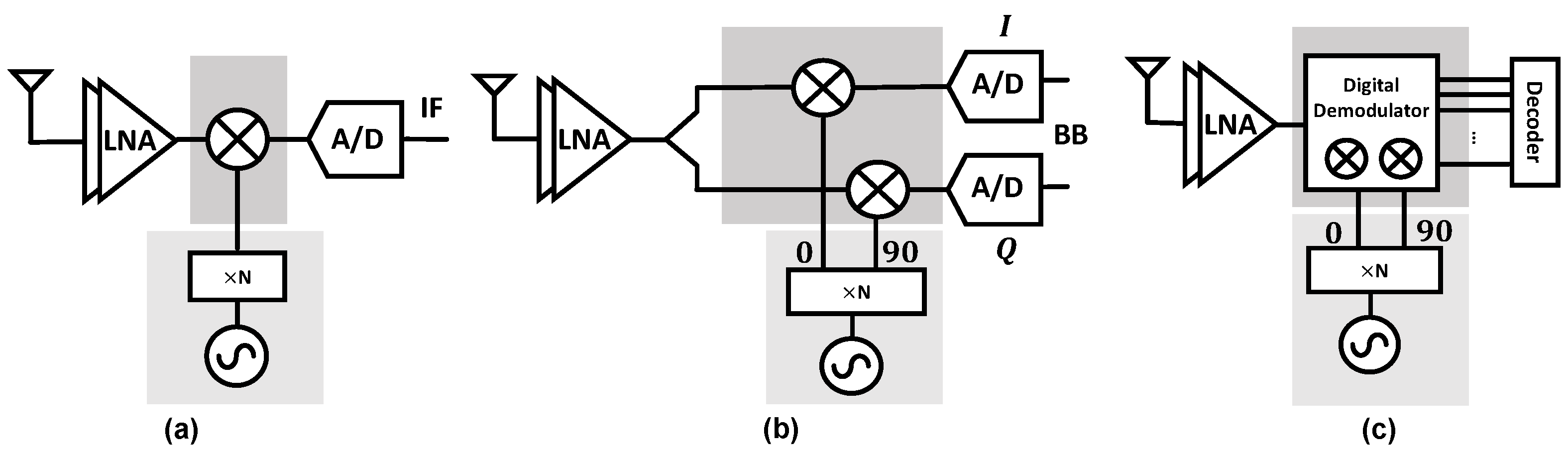
2.1. Heterodyne, Direct-Conversion, and Direct-Digital Modulation Transmitter

TX architectures in sub-THz communication systems are typically based on either traditional heterodyne (or multi-stage upconversion) designs or homodyne (direct-conversion) designs. In recent years, new architectures such as the direct-digital modulation transmitter have also been reported. Each method presents its own set of benefits and hurdles, especially as the operating frequencies approach sub-THz ranges. Figure 5 provides an overview of three primary architectures, which will be discussed in this section.
Heterodyne TX: In a heterodyne architecture (shown in Figure 5a), the signal generation process involves an intermediate frequency (IF) stage before final upconversion to the desired RF output. This approach allows the modulation to be performed at a lower frequency, where components such as mixers and modulators can achieve better linearity, accuracy, and stability [47,48,49]. One of the primary advantages of a heterodyne architecture is that it alleviates the need for the modulator to operate directly at sub-THz frequencies, which can be challenging and costly. For instance, achieving high linearity at sub-THz frequencies is more difficult than at a much lower IF, such as 100 MHz.
Nevertheless, heterodyne transmitters also come with trade-offs. In these systems, the complex-modulated IF signal requires higher resolution for accurate digitization or generation, as the IF signal contains precise amplitude and phase information. This level of detail is difficult to reproduce accurately and demands higher resolution components than those used in baseband (BB) generation. Furthermore, the multi-stage upconversion introduces potential challenges with image rejection and unwanted spectral components, which require filtering or complex frequency planning.
Homodyne TX: In contrast, homodyne, or direct-conversion transmitters, perform modulation directly from the baseband to the final RF output frequency, bypassing the need for an IF stage (shown in Figure 5b). Direct-conversion has gained traction in sub-THz applications because it offers a simpler architecture with fewer components, reducing power consumption and minimizing design complexity [11,12,13,50,51,52,53,54]. Direct-conversion simplifies signal generation by operating at baseband, where multi-level signals can be digitally generated with relative ease and transmitted directly to the output frequency. This design reduces power requirements and component count, making it highly suitable for compact, integrated sub-THz transmitters.
However, direct-conversion also has limitations. The lack of an IF stage requires high-precision mixers and modulators that can maintain linearity and spectral purity at sub-THz frequencies. Additionally, direct-conversion systems are susceptible to DC offset, I/Q imbalance, and LO feedthrough, which can degrade signal quality and reduce effective SNR. While digital pre-distortion and other calibration techniques can mitigate these issues, they add complexity to the system. In the context of complex-modulated signals such as 16 QAM, a homodyne system benefits from directly generated baseband signals that are easier to process, given that they contain only fixed amplitude levels without the added phase precision required in IF signals.
Direct-Digital Modulation TX (DDMT): DDMTs represent an innovative evolution in transmitter architectures for sub-THz communication, focusing on transforming bits directly into high-order modulation constellations (shown in Figure 5c). These transmitters bypass traditional components such as high-speed digital-to-analog converters by employing advanced modulation schemes to directly generate signals at the desired frequency using binary-weighted current-steering RF-DACs (shown in Figure 6, or other similar components), enabling high data rates with greater energy efficiency [14,55,56,57,58].
Recent advancements demonstrate the capability of DDMTs to achieve outstanding performance metrics. In addition to using RF-DACs, other methods of achieving direct-digital modulation have been reported. For example, a 135 GHz direct-modulation transmitter using separate bits for amplitude modulation and phase modulation on I/Q paths (shown in Figure 7a) achieved 16 QAM with 32 Gbps data rate, while consuming only 130 mW of DC power [59]. The design of the PAM2 amplitude and phase modulator is straightforward, which reduces the system overhead. Another design achieves 64 QAM with a data rate of 120 Gbps by summing the vectors of three QPSK outputs with different amplitudes, as shown in Figure 7b [17,60]. This method ensures flexibility in modulation schemes, allowing seamless transitions between QPSK, 16 QAM, or even higher-order modulation schemes based on the system SNR constraints. No power back-off is required for this design, which eases the output power limitation of the normal transmitter. The measured frequency spectrum, eye diagram, and constellation are shown in Figure 8. Furthermore, DDMTs inherently simplify the transmitter chain by eliminating IF stages and associated calibration challenges, thus reducing power consumption and system complexity. These results underscore the potential of DDMTs in meeting the demands of next-generation sub-THz wireless communication systems. However, direct modulation also introduces challenges related to limited signal-to-noise-and-distortion ratio (SNDR), I/Q mismatches, and higher sensitivity to EVM, which can impact the achievable modulation indexes. To address these limitations, techniques such as digital predistortion (DPD), adaptive biasing, and optimized circuit topologies are employed to improve signal integrity. Despite these challenges, recent implementations have demonstrated that direct modulation can support modulation schemes as high as 512 QAM with competitive power efficiency, making DDMTs a keystone technology for sub-THz wireless communication systems.
TX Above F max : For transmitter designs operating beyond the transistor’s f m a x (>200 GHz), three key topologies are employed: mixer-last, multiplier-last, and cubic-mixer-last architectures [61]. The block diagrams are shown in Figure 9. The mixer-last topology upconverts an IF signal to the target frequency using a mixer driven by a LO signal at high frequency, offering high linearity and supporting complex modulation schemes such as QAM, but at the cost of increased power consumption and circuit complexity [62,63]. The multiplier-last approach amplifies the modulated IF signal before multiplying it to the desired frequency, allowing PAs to operate in saturation for higher efficiency, but limiting modulation to constant-envelope schemes such as QPSK [39]. The cubic-mixer-last topology combines frequency multiplication and mixing by leveraging non-linearities (sub-harmonic mixer), reducing circuit complexity, and achieving efficient signal generation with moderate linearity [46]. Each topology represents a trade-off between efficiency, linearity, and modulation complexity, tailored to the challenges of sub-THz transmitter design.

2.2. Signal Generation: VCO vs. Frequency Multiplier

In high-frequency TX designs for sub-THz communication systems, LO signal generation poses a challenge in balancing phase noise, power efficiency, and spectral purity. Two primary approaches for generating high-frequency signals include using voltage-controlled oscillators (VCOs) directly at the target frequency (Figure 10a) or employing frequency multipliers to upconvert a lower-frequency signal (Figure 10b). Due to their superior phase noise characteristics and better energy efficiency, frequency multipliers are often preferred over direct high-frequency VCOs in sub-THz systems.
One of the main reasons for using frequency multipliers over high-frequency VCOs is the inherent phase noise characteristics. As frequency increases, achieving low phase noise directly through high-frequency VCOs becomes challenging due to the degradation of the quality factor (Q) of on-chip passive components, which results in higher phase noise levels [64]. Frequency multipliers, on the other hand, allow for the generation of a high-frequency signal from a stable, low-frequency VCO with minimal phase noise degradation. Phase noise is typically increased by 20 × log(N) dB, where N is the multiplication factor, but this still results in a lower noise profile than that of a high-frequency VCO operating directly at sub-THz frequencies [65]. Additionally, the use of frequency multipliers can lead to more power-efficient designs. High-frequency VCOs generally require substantial power to maintain oscillations at sub-THz frequencies, whereas frequency multipliers consume less power by amplifying and selectively filtering other harmonics generated from lower-frequency signals.
Phase noise directly affects the EVM and, consequently, the achievable modulation index. For advanced modulation schemes such as 16 QAM or 64 QAM, low phase noise is critical for maintaining signal fidelity. The low phase noise of the frequency multiplier facilitates the use of higher modulation indices by providing a cleaner LO signal and supporting robust high-order modulation without degrading signal quality [64].
In summary, the preference for frequency multipliers over direct high-frequency VCOs in sub-THz TX designs stems from a strategic trade-off between phase noise reduction, power efficiency, and support for high-order modulation. Sub-THz systems are capable of achieving the requisite spectral purity and phase noise characteristics crucial for high-capacity wireless communication by producing high-frequency signals via multipliers.

2.3. Phase Shifter

I/Q generation in sub-THz transmitter designs, accurate phase rotation between in-phase (I) and quadrature (Q) signal paths is crucial for effective modulation and demodulation, particularly in systems using QAM. This phase difference, typically set at 90 degrees, can be achieved using three primary methods: couplers, poly-phase filters, and delay lines. Each approach offers unique trade-offs in terms of frequency range, precision, and integration complexity.
Couplers: Couplers are widely used in high-frequency systems to split an input signal into two signals with a 90-degree phase shift, producing the required I/Q components (Figure 11a). A commonly used coupler in I/Q generation is the quadrature hybrid coupler, which can achieve a stable 90-degree phase shift over a specified bandwidth [15,39,51,66,67]. Couplers are particularly effective for wideband systems, as they offer consistent phase accuracy across a broad frequency range. However, implementing couplers in sub-THz systems can be challenging due to size constraints and the need for low insertion loss. High-frequency couplers also require precise manufacturing, as even minor mismatches in the design can lead to phase errors that degrade the signal quality.
Delay lines: Delay lines provide a third approach to achieve the required phase difference between the I and Q paths by introducing a time delay to one of the signal paths [12,30]. This delay corresponds to a phase shift, which can be tuned to a certain degree by adjusting the line length or delay element configuration (Figure 11b). Delay lines are advantageous in that they can be adjusted dynamically, allowing phase tuning at different frequencies. However, implementing delay lines at sub-THz frequencies is challenging due to the precise length and low-loss requirements needed to maintain signal integrity. Furthermore, delay lines consume a large silicon area, which is a limiting factor in highly integrated systems.
Poly-phase filters: Other phase-shifting approaches include poly-phase filters (PPFs) [68] and switchable phase shifters (SPSs) [40]. PPFs are passive networks that use resistors and capacitors arranged in a configuration that splits the signal into two paths with a phase difference of 90 degrees. The advantage of poly-phase filters lies in their compact design and low power consumption, making them ideal for integrated circuit applications where space and power efficiency are priorities. SPSs comprise L-C networks and single-pole dual-throw (SPDT) switches that control the phase shift by bits (Figure 11c). However, PPFs typically have a limited bandwidth, as their phase accuracy depends on the matching of passive components, which can vary with frequency. This limitation makes these methods more suitable for applications with a fixed or narrowband frequency requirement.
Digital-controlled transmission line: Digital-controlled transmission lines provide precise phase manipulation essential for high-frequency communication systems. These phase shifters adjust phase shifts digitally, allowing for fine control with minimal analog tuning complexity. The fundamental principle relies on switched transmission lines or lumped-element networks, where digital control signals toggle the phase shift stages to achieve the desired phase states [69]. An example model of the digital-controlled phase shifters is shown in Figure 12 where the switches control the dielectric constant of the transmission line and thus the electrical length. Recent advances have focused on improving resolution, minimizing insertion loss, and achieving low power consumption. For instance, a compact D-band phase shifter achieves 0.1-degree phase resolution with an RMS phase error of 0.8 degrees [70]. Additionally, a low-loss digital-controlled transmission line in 45 nm RF-SOI technology implements a trombone-like structure, enabling calibration-free operation with a phase tuning range of 360 degrees and an insertion loss of 11.5 dB [71]. Though increasing digital control complexity, these innovations highlight state-of-the-art developments in digital phase control, enabling high-performance beam-forming and precise calibration for next-generation wireless communication systems.
In conclusion, each method for phase shifting and I/Q generation presents specific advantages and trade-offs, and the optimal choice depends on the application’s requirements for bandwidth, power efficiency, and integration level. By selecting the appropriate phase shifting technique, sub-THz TX designs can achieve the necessary phase accuracy for effective modulation and signal integrity across various frequency ranges.

2.4. Power Amplifier

Sub-THz power amplifiers (PAs) are crucial components in sub-THz transmitters, responsible for boosting signal power to levels necessary to overcome high free-space path loss and ensuring reliable communication links. The design of sub-THz PAs faces challenges related to efficiency, linearity, and integration, particularly at high frequencies. The trend of saturated power ( P s a t ) of sub-THz PA with various technologies is plotted in Figure 13, where a boundary of around 25 dBm is illustrated.
PA Topologies: Three common PA topologies used in mm-Wave designs are power-combining, Doherty, and output-phasing architectures.
Due to the limited output power capability of individual transistors, power-combining techniques are often employed to increase the total output power. Power combiners aggregate the output from multiple amplifier stages, using methods like current combining, Wilkinson combiners, or transformer-based combining. For instance, two-way to eight-way current-combining architecture demonstrated in sub-THz PA efficiently increases output power by leveraging symmetrical transformer-based or coupled-line coupling, which reduces sensitivity to parasitics and enhances power delivery [18,19,73,74,75,76]. The block diagrams of two commonly used power combination topologies based on current and voltage are shown in Figure 14 [77,78]. Additionally, multi-drive stacked-FET approaches utilize series-stacked transistors to support higher voltage swings, achieving higher output power while maintaining device reliability in advanced CMOS processes [79,80].
The Doherty power amplifier (DPA) is widely used for its ability to enhance power efficiency, particularly at back-off power levels. In a DPA, the main and auxiliary amplifiers operate in tandem to optimize efficiency across a range of output power levels. mm-Wave DPAs have been demonstrated in the E-band [81], but the transformer-based power-combining network becomes lossy at sub-THz frequencies. To mitigate this issue, DPAs that operate at higher frequencies apply a distributed network to enhance efficiency [74].
Outphasing PAs, or LINC (linear amplification using non-linear components), split the input signal into two phase-modulated components. These components are amplified separately and then recombined at the output, achieving high linearity and efficiency. The output-phasing technique is beneficial for high-order modulation schemes as it reduces the effects of amplitude distortion by relying on phase modulation, making it well suited for sub-THz transmitters that use complex modulations such as 16 QAM and 8PSK [20,21].
PA’s Non-linearity: Non-linearity in PAs is a critical concern at mm-Wave frequencies, as it directly affects signal quality and modulation performance. The primary non-linear effects include the 1 dB compression point O P 1 dB , amplitude-to-amplitude (AM/AM) distortion, and amplitude-to-phase (AM/PM) distortion [82].
The O P 1 dB point indicates the output power level at which the amplifier gain drops by 1 dB due to saturation effects. It serves as a key metric for PA linearity, especially at high frequencies, where maintaining a high O P 1 dB is challenging due to reduced transistor breakdown voltages. In recent D-band PA designs, gain expansion techniques have been employed to push O P 1 dB to 20.4 dBm while maintaining high efficiency [83].
AM/AM distortion refers to the non-linear relationship between input amplitude and output amplitude, while AM/PM distortion involves undesired phase shifts as a function of input amplitude. Both types of distortion degrade the signal quality, affecting the EVM and reducing the achievable modulation indexes [84]. An illustration of these two non-linearities’ effect (together with AWGN) on the constellation is shown in Figure 15. In sub-THz PAs, stacked-FET architectures and adaptive biasing are often used to mitigate these non-linear effects by providing a more linear amplification profile and stabilizing the phase response across varying input levels [79].
Digital Calibration Techniques: To address the non-linearity and efficiency challenges in mm-Wave PAs, digital calibration techniques have become an integral part of modern PA design. Digital pre-distortion (DPD) is a widely used technique to linearize PAs by applying an inverse distortion function to the input signal, pre-compensating for the PA’s inherent non-linearity. DPD algorithms adaptively adjust the input signal to minimize AM/AM and AM/PM distortions, significantly improving linearity and enabling the use of high-order modulation schemes. Recent designs implement DPD using low-latency digital signal processing blocks integrated directly into the baseband circuitry of the transceiver, allowing real-time calibration [85].
Thermal effects can cause performance degradation in PAs, particularly in high-power and high-frequency applications. Thermal management techniques such as dynamic biasing and active cooling help manage the heat generated by the PA, stabilizing its performance. Dynamic biasing adjusts the bias current based on temperature feedback, optimizing efficiency while preventing device breakdown under high currents [85,86].
Dynamic biasing involves adjusting the operating point of the amplifier in real time to optimize performance based on signal power and environmental conditions [87]. This approach improves efficiency, particularly at lower output power levels, by reducing the bias current when full power is not needed. It is especially effective in stacked-FET PAs, where it helps manage voltage stress and ensures consistent performance across varying supply voltages and temperatures.

3. Receiver Design Considerations and Challenges

A summary of the performance of the sub-THz wireless communication link receiver, including data rate, modulation schemes, and receiver noise figure (NF) and conversion gain (CG), is presented in Figure 16. More than 60 data points have been analyzed, most of which are collected from works published over the past five years to highlight the latest advances in receiver technology. The highest data rate achieved is 128 Gbps in the D-band [88]. For modulation schemes, the most frequently reported is QAM, the highest level being 2048 QAM in the W-band with a passive mixer and an IF amplifier [58], 512 QAM achieved by an ultra-wideband dual receiver system in the D-band [47], and 32 QAM in the J-band [89]. NF is reported to range from 4.7 dB [90] to 15 dB in most receiver designs, with lower values achieved in systems optimized for specific narrowband applications. There are also receivers on multi-channel communication in sub-THz [45]. CG is observed in the range of 20 to 40 dB in most receiver architectures, with a noticeable reduction at higher frequencies. An observable trend is the increase in NF accompanied by a reduction in CG as the operating frequency increases above 200 GHz.
This section will introduce the system design considerations for sub-THz receivers, including the classical heterodyne and homodyne architectures, direct-digital demodulation, and other advanced receiver concepts.

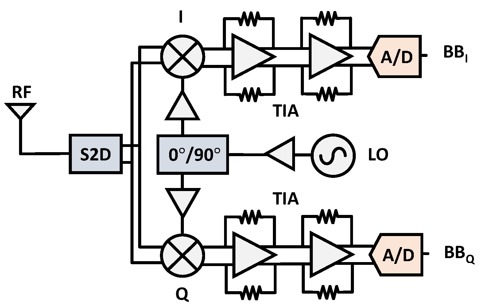
3.1. Heterodyne and Homodyne Receiver

The block diagrams for the heterodyne, homodyne and direct-digital demodulation receivers are shown in Figure 17. The heterodyne architecture is popular, particularly for D-band applications [50,89,91,92,93,94]. Heterodyne receivers typically use a single mixer and a lower LO frequency, which helps minimize signal loss and noise gain. Furthermore, the use of a single mixer improves image frequency rejection, which is particularly important in the D-band, where image frequency interference is a significant concern. In the design of heterodyne receivers, the quality of the LO signal is a critical consideration, as phase noise and linearity significantly affect the overall performance of the receiver. These factors are important in both heterodyne and direct-conversion (zero-IF) architectures, but heterodyne systems require particular attention to the selection of IF and LO frequencies. In heterodyne systems, the selection of the IF is crucial. The choice of IF should be made with precision to ensure compatibility with both RF and LO frequencies, aiming to minimize any LO leakage into the RF and IF bands and to attain strong image rejection. For instance, in a D-band receiver, an IF range of 26–34 GHz is selected. This choice is based on its near compatibility with existing 5G FR2 chips, facilitating further down-conversion of the IF signal to baseband [23].
Due to the simplicity of the system, the homodyne architecture (direct-conversion) is attractive for achieving compact and low power in receiver design [95,96,97]. One of the key advantages of direct-conversion is the ability to convert the RF signal directly to baseband, avoiding the complexities associated with IF stages. This reduces the number of components required, simplifies the overall design, and improves the system’s power efficiency. Furthermore, direct-conversion minimizes the risk of image frequency interference, as it directly converts the RF signal to the baseband without additional mixing stages that could generate image frequencies. This is especially useful in systems where eliminating image frequency interference is crucial. Despite the advantages of direct-conversion, its application in high-frequency bands such as the D-band presents several challenges.
For example, the generation and distribution of I and Q components in the LO waveform are particularly demanding at high frequencies. Quadrature systems suffer from significantly higher phase noise—up to 12.6 dB higher compared to differential topologies—and consume more power. Additionally, I/Q mismatches at frequencies like 300 GHz require extremely precise timing alignment. For example, a phase mismatch of 10° translates to approximately 45 fs, making direct-conversion architectures especially difficult to implement effectively [91].
In D-band applications, dual down-conversion architectures are used to optimize receiver performance [24]. Compared to traditional single-stage down-conversion, dual down-conversion offers several advantages such as improved image ejection, bandwidth expansion, and design flexibility as it allows adjustments to be made based on application requirements and frequency characteristics.

3.2. LNA-First Versus Mixer-First Architectures

LNA-First RX: In receiver designs, the LNA-first architecture is a majority choice due to its excellent noise performance at the front-end of the receiver chain. The LNA, as the first component in the signal chain, plays a critical role in amplifying weak signals while maintaining a low NF, which is crucial to improving receiver sensitivity. With low NF and high gain of LNA, the following blocks in the RX path have less stringent NF requirements, as indicated by the Friis equation. LNA-first designs have demonstrated strong performance across various frequency bands.
However, while the LNA-first architecture excels in terms of noise performance, it also introduces inherent challenges, particularly in linearity and blocker suppression. The LNA amplifies all signals, including strong interfering signals (blockers), which diminishes the receiver’s dynamic range. Specifically, when subjected to strong signals, the LNA can enter a non-linear region, resulting in signal distortion. This leads to a decrease in the 1 dB compression point ( I P 1 d B ), limiting the receiver’s ability to handle high-power signals (equivalently reducing the dynamic range) [98].
Mixer-First RX: The mixer-first architecture, in which the mixer is placed at the front-end of the receiver chain to enable direct down-conversion of the received signal, was initially proposed to address wideband impedance matching challenges in broadband receivers [99,100,101,102] (Figure 18). In the sub-THz range, it effectively mitigates the limitations of LNA-first designs, particularly in terms of linearity and blocker suppression. By shifting the signal to a lower IF early in the signal chain, this architecture allows the system to tolerate higher levels of blocker interference, thereby reducing the stringent linearity requirements typically imposed on high-frequency stages.
Furthermore, mixer-first architectures are particularly advantageous in high-frequency ranges, where maintaining low NF in the LNA becomes increasingly challenging. For 28 nm CMOS technology, the upper-frequency limit is typically around 280 GHz, and as the frequency approaches half of this value, the performance of active parts such as the LNA deteriorates significantly. In sub-THz, further compromising LNA performance. As a result, many designers opt for mixer-first architectures at these higher frequencies to avoid the inherent limitations of LNA performance [103].

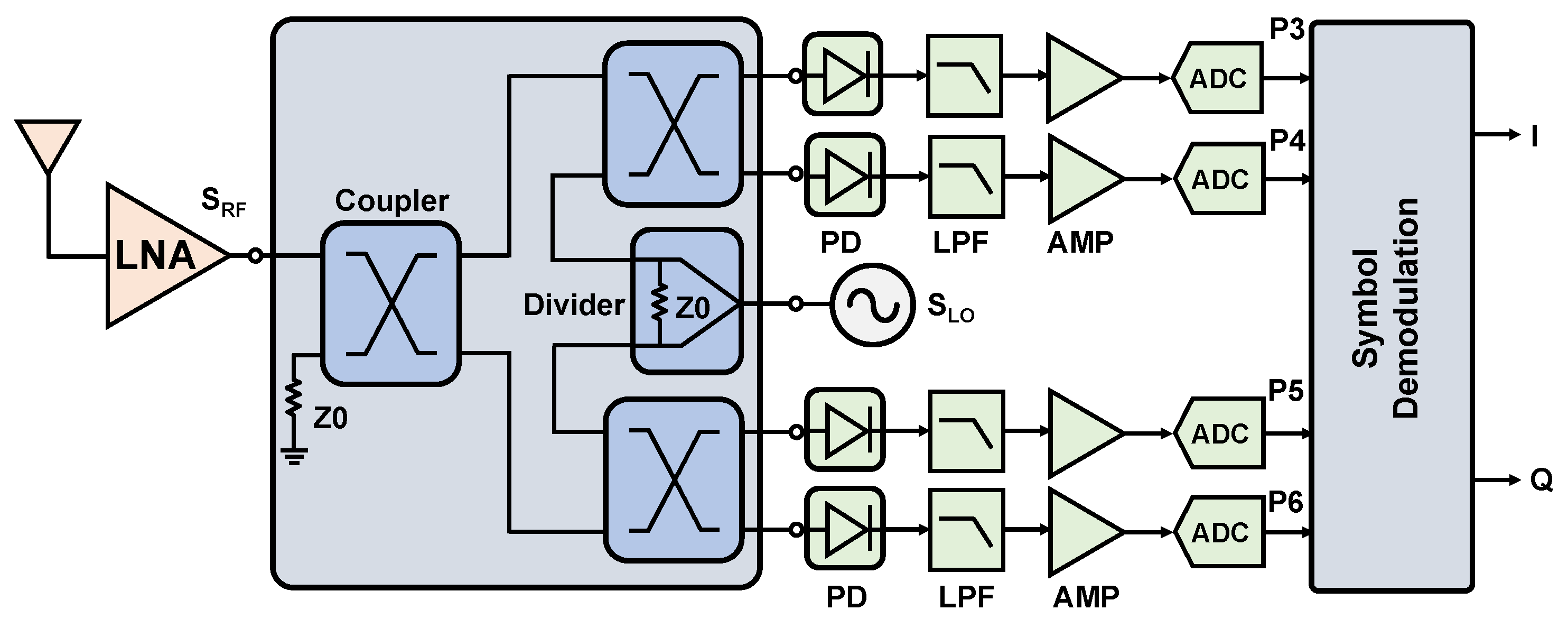
3.3. Direct-Demodulation Receiver

Demodulation plays a critical role in communication systems by extracting transmitted data from received signals. Traditional demodulation techniques typically rely on high-speed ADCs to digitize received analog signals, followed by complex digital signal processing (DSP) to decode transmitted information. However, as the demand for higher data rates increases, particularly for advanced modulation schemes, these conventional ADC-based demodulation methods encounter significant challenges such as high power consumption and system complexity.
In response to these challenges, direct demodulation receivers have emerged as a viable solution, offering significant reductions in power consumption and complexity. Direct analog demodulation techniques bypass the need for high-speed ADCs by extracting amplitude and phase information directly from the received analog signal. For example, methods such as NR-STAR-MQAM use analog circuitry, such as root-square computation to determine the amplitude ( d r ) and a phase detector to extract the phase ( ϕ r ), enabling a compact and low-complexity circuit design. These techniques significantly reduce power consumption—up to 31 times lower than digital methods—while maintaining comparable error performance [104]. By simplifying the receiver architecture, direct demodulation enables ultra-high-speed communication in sub-THz systems while addressing key limitations of traditional ADC-based designs.
Recent innovations have introduced RF-correlation-based direct-demodulation methods, which offer a more efficient and power-effective alternative for high-order modulations such as 8PSK. This method leverages multi-phase RF correlation to directly demodulate 8PSK symbols, eliminating the need for high-speed ADCs and complex digital processing. As described in the work of [105] (Figure 19), the proposed method involves correlating the received signal with multiple phase-shifted versions of the local oscillator (LO) signal. This process allows the system to detect the phase of the received signal without relying on amplitude-based decisions. Using simple sign-check comparators (e.g., BPSK decision logic), the system can detect symbols with significantly lower power consumption and reduced hardware complexity. The approach is particularly beneficial in high-frequency applications, such as mm-Wave communication, where traditional high-speed ADCs are not only power hungry but also require significant computational resources.
One key advantage of the RF-correlation-based method is its tolerance to phase errors. Even if the LO phase deviates from the ideal angle by up to 22.5°, the system can still accurately detect the symbols. This robustness to phase errors is a critical improvement over conventional methods, where small phase deviations can lead to substantial errors in symbol detection. Moreover, by reducing the dependence on high-speed ADCs, this method enhances the sensitivity and linearity of the receiver, making it suitable for ultra-high-frequency applications.
Recent research has shown that ADC-less demodulation techniques can also be applied to QAM modulation schemes, offering a promising solution for low-power and efficient receiver designs. Conventional QAM receivers typically require ADCs to sample the I and Q channels and subsequent digital processing. In the architecture shown in Figure 20, it reduces hardware complexity by amplitude and phase detector on the I and Q paths. However, this method is restricted to lower modulation schemes; with higher modulation indices, the amplitude and phase resolution exceed the capabilities of the detectors, and the BER will increase as a result.
Six-Port Direct-Demodulation Receiver: Another type of direct-demodulation receiver employs the six-port theory, or the so-called linear interferometric technique, offering distinct advantages over traditional non-linear mixer-based architectures like homodyne and superheterodyne systems [106,107,108]. These advantages include low power consumption, simple and compact configuration, wideband performance, and robustness to power-level variations. The six-port receiver fundamentally operates on the principle of linear interference, utilizing passive networks of hybrid couplers, power dividers, and power detectors to superimpose the received RF signal and LO under controlled phase conditions. The relative amplitude and phase shifts of the input signals at the various ports allow the direct extraction of components I and Q without requiring high-speed ADCs or complex digital signal processing (Figure 21).
The six-port receiver operates by linearly combining the RF input signal S RF and the LO signal S LO through a passive network. The equations for S RF and S LO are given as follows:
S RF ( t ) = A RF cos ( ω RF t + ϕ RF ) ,
S LO ( t ) = A LO cos ( ω LO t ) .
The output voltages at the four power detectors are functions of the relative amplitudes and phases of these signals. The six-port junction linearly combines the input signals with specific phase shifts θ k for each port k and the output power at the k-th port is proportional to the square of the voltage. The voltage and power at the k-th port can be derived as follows:
V k ( t ) = S RF ( t ) + S LO ( t + θ k ) ,
P k = | V k | 2 = 1 2 A RF 2 + A LO 2 + 2 A RF A LO cos ( ϕ RF + θ k ) .
Then, the I and Q components can be derived from differences in power at the ports:
I = P 3 P 5 = 2 A RF A LO cos ( ϕ RF ) ,
Q = P 4 P 6 = 2 A RF A LO sin ( ϕ RF ) .
Recent innovations, such as joint multiband receivers, extend the six-port architecture’s utility by enabling concurrent operations at sub-THz frequencies [109], combining signals from both domains into a unified platform. These systems leverage the six-port receiver’s ability to simultaneously handle modulated signals across diverse frequency bands with minimal power consumption and straightforward hardware.
Kramers–Kronig Receiver: The Kramers–Kronig (KK) receiver is a direct-demodulation approach that simplifies coherent signal reception by eliminating the need for a high-frequency LO and mixers [110,111]. Instead, it takes advantage of the mathematical relationship between the amplitude and phase of an analytic signal. This technique, adapted from optical communication, is particularly effective for wireless systems operating at terahertz frequencies, offering significant advantages in simplicity and power efficiency.
An analytic signal U ( t ) can be expressed as follows:
U ( t ) = U 0 + U s ( t ) ,
where U 0 is a strong carrier and U s ( t ) represents the data signal. The KK receiver ensures that U ( t ) satisfies the minimum-phase condition:
| U s ( t ) | < U 0 ,
such that the amplitude | U ( t ) | contains sufficient information to reconstruct the phase ϕ ( t ) . The phase can be recovered using the Kramers–Kronig relation:
ϕ ( t ) = 1 π P ln | U ( τ ) | t τ d τ ,
where P represents the Cauchy principal value.
The KK receiver employs an envelope detector, such as a Schottky barrier diode (SBD), to measure the amplitude | U ( t ) | . Advanced digital signal processing (DSP) techniques are then used to reconstruct the phase ϕ ( t ) and demodulate the signal. An example is shown in Figure 22. This approach is compatible with advanced modulation schemes, such as 16 QAM, and enables high data rates, achieving up to 115 Gbps over significant distances (e.g., 110 m [111]). The simplified architecture of the KK receiver reduces both power consumption and hardware complexity, making it an ideal candidate for sub-THz wireless networks.

4. Transceiver System Design

4.1. System Considerations: Full Duplex with Single/Double Antenna, SIC, and LO Feedthrough

In sub-THz and mm-Wave transceiver (TRX) systems, one of the critical design choices is the implementation of full-duplex communication, which enables simultaneous transmission and reception of signals. Achieving efficient full-duplex operation in these high-frequency systems requires careful consideration of antenna configurations, self-interference mitigation, and LO feedthrough suppression. Two common configurations in full-duplex systems are single-antenna and double-antenna configurations, each presenting unique trade-offs in terms of isolation, integration, and system complexity.
Single-antenna full-duplex systems use a shared antenna for both TX and RX paths, typically employing an SPDT switch to alternate between transmit and receive operations [30,47]. This configuration offers the advantage of reduced size and integration complexity, making it particularly suitable for compact, highly integrated TRX systems at mm-Wave frequencies. However, single-antenna configurations face significant challenges related to self-interference. The high power of the transmitted signal can easily saturate the receiver front-end if adequate isolation is not maintained. To address this problem, self-interference cancellation (SIC) methods are utilized in the antenna, RF, and digital domains.
Recent works on sub-THz full-duplex phased-array transceivers have demonstrated SIC by employing a combination of analog and digital methods. Analog SIC is primarily achieved through directional couplers or cancellation loops that generate a replica of the transmitted signal and subtract it from the received signal. This approach effectively suppresses self-interference at the RF front-end, preventing receiver saturation. Digital SIC, on the other hand, further refines cancellation by leveraging adaptive filtering and signal processing algorithms to mitigate residual interference in the baseband domain.
For instance, a sub-THz full-duplex phased-array transceiver demonstrated effective self-interference cancellation using a combination of analog domain suppression and digital signal processing, achieving over 60 dB of cancellation without degrading the received signal quality. It typically involves the use of directional couplers or cancellation loops that subtract a copy of the transmitted signal from the received signal, while digital SIC leverages adaptive filters and signal processing algorithms to further suppress residual interference [112]. An example TRX work using SIC is shown in Figure 23, which achieves more than 20 dBc suppression of interference.
Another key issue in single-antenna systems is LO feedthrough, where the local oscillator signal leaks into the transmit or receive path, creating unwanted spurs and thus degrading the SNR. LO feedthrough can be exacerbated in direct-conversion transceivers, where the LO signal is mixed directly with the baseband signal. Techniques such as differential signal routing, improved LO buffering, and feedthrough compensation circuits have been implemented to mitigate these effects [112,113].
Double-antenna configurations utilize separate antennas for the TX and RX paths, inherently providing greater isolation between transmitted and received signals [114,115,116]. This approach reduces the impact of self-interference and allows for a higher dynamic range and better receiver sensitivity. The physical separation of TX and RX antennas can be particularly beneficial at sub-THz frequencies, where high-gain directional antennas are employed to counteract significant path loss.
Although double-antenna configuration is common, it also introduces challenges related to integration and size, particularly in compact, wafer-scale designs. Recent advances in TRX integration for full duplex TRx involve flip-chip bonding [56] and on-chip antenna arrays, allowing for high-density packaging without compromising performance. This approach was successfully demonstrated in a D-band radio-on-glass module, which integrated separate TX and RX with advanced packaging techniques, achieving stable performance across a wide frequency range [35].
In the most recent sub-THz transceiver works, TX and RX use a correlated LO signal to cancel phase noise and achieve a higher data rate or modulation scheme [15,50,117]. However, synchronized LO signal increased system complexity and does not apply to all wireless communication scenarios [118]. Instead, a recent work has reported 256 QAM with 8 Gbps in the D-band with uncorrelated TX and RX, which is shown in Figure 24 [35].
In summary, as the mm-Wave and sub-THz TRX systems aim for higher data rates and efficient full-duplex communication, significant progress has been made to address issues like self-interference and LO feedthrough, as analyzed in this section. Both single- and double-antenna configurations have their advantages, and the optimal choice depends on a combination of factors, including chip size, power budget, data rate constraints, isolation requirements, integration complexity, and overall system performance trade-offs to best suit the intended application.

4.2. Phased-Array System and Beam-Forming

Phased-array systems have become a key component in high-frequency transceiver designs, particularly in mm-Wave and sub-THz applications. The ability to electronically steer the beam without physically moving the antenna enables high-gain, directional transmission and reception, which is crucial for overcoming significant free-space path loss at these frequencies. Phased-arrays offer enhanced link performance through adaptive beam-forming, spatial multiplexing, and interference management, making them integral to modern wireless communication systems targeting 5G, 6G, and beyond.
The deployment of phased-array systems plays a crucial role in overcoming the inherent challenges associated with high path loss at sub-THz frequencies. The Friis transmission equation is widely used as follows:
P r = P t + G t + G r + 20 log 10 λ 4 π D ,
where the last term represents the free-space path loss in logarithmic scale. As frequencies increase, free-space path loss follows a quadratic relationship with frequency, significantly impacting the signal strength over long distances. To mitigate this effect, phased-array antennas leverage beam-forming techniques to focus radiated power in specific directions, effectively increasing the link gain and compensating for path loss.
Beam-forming in phased-array systems is achieved by controlling the relative phase of the signals fed to each antenna element. By introducing a phase shift to the signals of individual elements, the array can direct the beam in a specific direction, effectively focusing the signal energy and enhancing the received signal strength. It not only increases EIRP but also mitigates the impact of multi-path fading in dense environments [119,120].
Phased-arrays typically employ three primary beam-forming approaches: analog, digital, and hybrid beam-forming. In analog beam-forming, phase shifters or delay elements adjust the phase of the RF signal before transmission or reception, allowing for a compact and power-efficient design. However, analog beam-forming has limited flexibility, as the beam can only be steered in one direction at a time. Digital beam-forming, on the other hand, processes signals in the digital domain, allowing for simultaneous multi-beam steering and improved interference mitigation [8,121,122]. Hybrid beam-forming applies both analog and digital approaches with more complex TRX architectures.
Phased-array TRX systems can be implemented using several architectural approaches, including RF beam-forming, IF beam-forming, and LO beam-forming. Each architecture offers unique trade-offs in terms of complexity, power efficiency, and beam-forming capabilities. The block diagrams of those architectures are shown in Figure 25.
RF Beam-forming: In RF beam-forming, the phase shift is applied directly to the RF signal using phase shifters or delay lines [30,34,47,92,123]. This approach minimizes the number of required data converters, reducing power consumption and hardware complexity. However, RF beam-forming typically lacks the flexibility needed for advanced multi-beam steering. A recent example of an RF beam-forming system is the D-Band 8×8-Element transmit–receive arrays that achieved an angular range of 60 degrees in the H plane and 38 degrees in the E plane [47]. The measured 2D and 3D patterns are shown in Figure 26 with a sidelobe level (SLL) of 12.5 dB.
IF Beam-forming: IF beam-forming applies phase shifts at the IF stage, allowing better control of the signal phase before it is upconverted to the RF frequency [49,93,124,125,126]. This method offers a compromise between the simplicity of RF beam-forming and the flexibility of digital beam-forming. IF beam-forming systems can achieve efficient multi-beam operation while reducing the phase shifter’s frequency dependency. A recent D-band TRX system used IF beam-forming to provide efficient phase control across a wide frequency range, supporting high-data-rate communication with robust beam steering capabilities.
LO Beam-forming: Similarly, if a phase change occurs on the LO path, then this method is called LO beam-forming [127,128]. LO beam-forming avoids additional loss on the signal paths and causes minimal gain variations. However, steering the phase at sub-THz frequencies requires a large amount of power, and phase error is another area of concern.
Other Challenges: Designing efficient phased-array TRX systems for mm-Wave and sub-THz applications involves several challenges, including phase noise, mutual coupling between antenna elements, and calibration of phase and amplitude mismatches.
At sub-THz frequencies, phase noise is a significant issue that can degrade the signal quality and limit the achievable data rate. High phase noise affects the beam’s coherence, reducing the effective gain and increasing the EVM. To mitigate phase noise, recent phased-array designs employ low-noise VCOs coupled with frequency multipliers, alongside digital calibration techniques that dynamically correct phase errors. For instance, a 60 GHz phased-array TRX system integrated adaptive phase noise compensation to enhance beam coherence and improve modulation fidelity in high-order QAM schemes.
Mutual coupling between closely spaced antenna elements can distort the beam pattern and reduce overall system performance. This coupling leads to unwanted changes in the impedance of each antenna element, which impacts the phase and amplitude response. Techniques such as decoupling networks, spatial filtering, and optimized array layouts have been employed to reduce mutual coupling.
The precise calibration of phase and amplitude mismatches is essential for maintaining beam-forming accuracy. Small errors in phase and amplitude can significantly distort the beam pattern, reducing the array’s effective gain and limiting the achievable data rate. Digital calibration methods, such as least mean squares (LMS) algorithms and adaptive equalization, are commonly used to dynamically adjust phase and amplitude errors.
In conclusion, phased-array systems are integral to modern mm-Wave and sub-THz TRX designs, offering enhanced beam-forming and spatial multiplexing capabilities. Using advanced beam-steering techniques and addressing associated design challenges, phased-arrays enable robust, high-performance communication links in next-generation networks.

4.3. MIMO Systems

Multiple-input multiple-output (MIMO) technology offers a robust solution to achieve high data rates in the sub-THz frequencies [31,121,129]. By utilizing multiple antennas at both the transmitter and receiver, MIMO enables the simultaneous transmission of multiple independent data streams over the same frequency band, effectively increasing spectral efficiency and enhancing link reliability through spatial diversity. An example photo of 4 × 4 MIMO measurement achieving a total data rate of 640 Gbps is shown in Figure 27. By employing spatial multiplexing, MIMO allows the simultaneous transmission of multiple independent data streams over the same frequency resources, significantly enhancing spectral efficiency. Furthermore, MIMO’s diversity gain plays a crucial role in ensuring link reliability and robustness in multipath environments. By receiving diverse copies of the transmitted signal, diversity gain mitigates the effects of deep fading and multipath interference, enhancing the system’s resilience to channel impairments.
In particular, Choi et al. explored the use of concurrent 20-beam transmission to significantly enhance spatial multiplexing efficiency while maintaining low power consumption [130]. A key contribution of this work is the implementation of a joint static/dynamic beam-forming system that combines static phased-array techniques with dynamic space–time modulation. Through the integration of these technologies, our work not only advances the state of the art in high-frequency MIMO systems but also lays the foundation for scalable, low-cost sub-THz communication infrastructures suitable for future wireless standards.

5. Conclusions

In this paper, we reviewed the latest advancements in sub-THz transceiver architectures, covering high-frequency signal generation, power amplifier design, direct modulation schemes, phased-array beam-forming, and MIMO technologies. While significant progress has been made, several challenges remain in realizing practical sub-THz communication systems.
One of the primary obstacles is the commercialization and standardization of sub-THz technology. Regulatory bodies such as the FCC have initiated efforts to allocate spectrum and define standardization frameworks. However, industry-wide collaboration is still required to ensure interoperability, efficient spectrum utilization, and cost-effective semiconductor solutions. Despite ongoing developments, the adoption of sub-THz communication is currently constrained by fabrication costs, energy efficiency limitations, and the complexity of high-frequency circuit integration. Future research must address these barriers by developing scalable semiconductor processes, advanced packaging techniques, and energy-efficient system architectures.
From a technical perspective, data rates and modulation schemes in sub-THz communication have been pushed close to the limits of thermal noise and transistor performance. As further improvements yield diminishing returns, research should shift toward enhancing power efficiency rather than solely increasing data rates. The development of direct-digital modulation transmitters and direct-digital receivers introduces new opportunities to optimize energy efficiency and system complexity. In terms of the building blocks, digital-controlled transmission lines are becoming key elements that offer improved phase tuning precision compared to conventional passive phase shifters. Additionally, PA efficiency at sub-THz frequencies remains a major bottleneck. Innovations in PA architectures, outphasing, and load modulation are required to enhance P s a t and power-added efficiency (PAE). Transceiver design techniques, such as the self-interference cancellation, can further enhance the overall performance of the system. Lastly, the widespread adoption of phased-array and MIMO architectures at sub-THz frequencies will be essential to overcome propagation challenges and enable high-capacity wireless links. Techniques such as hybrid beam-forming could provide a practical trade-off between performance and power consumption. Together, these methods pave the path for the next-generation wireless communication system.
Addressing these commercial, regulatory, and technical challenges will be crucial for bridging the gap between academic research and real-world deployment. Although this work provides a comprehensive review of advanced sub-THz transceivers, it has certain limitations. This study primarily focuses on circuit- and system-level advancements in sub-THz TRX design. However, other crucial aspects, such as advanced semiconductor technologies that enable these circuits, have not been extensively covered. Furthermore, measurement techniques, including vector network analyzers (VNAs), oscilloscopes, and spectrum analyzers, play a fundamental role in the characterization and validation of sub-THz transceivers but are beyond the scope of this work. Furthermore, on-chip antennas and packaging technologies, which are integral to the practical implementation of sub-THz transceivers, warrant further exploration. Future work could provide a more detailed discussion of these topics to offer a more holistic perspective on the development and deployment of sub-THz wireless communication systems. As semiconductor technologies and circuit design techniques continue to advance, sub-THz wireless communication is expected to play a critical role in future sub-THz wireless networks, unlocking new possibilities for high-speed connectivity and ultra-low-latency applications.

Author Contributions

Conceptualization, R.C.; Coordination, R.C. and M.-C.F.C.; Writing— original draft, R.C.; Writing—review and editing, R.C. and B.Y. All authors have read and agreed to the published version of the manuscript.

Funding

This research received no external funding.

Data Availability Statement

Not applicable.

Conflicts of Interest

The authors declare no conflicts of interest.

Abbreviations

List of Terms and Acronyms.
AcronymFull Term
ADCAnalog-to-Digital Converter
AM/AMAmplitude Modulation to Amplitude Modulation Distortion
AM/PMAmplitude Modulation to Phase Modulation Distortion
APSKAmplitude Phase Shift Keying
BERBit Error Rate
BBBaseband
CMOSComplementary Metal-Oxide-Semiconductor
DACDigital-to-Analog Converter
DDMTDirect-Digital Modulation Transmitter
DPDDigital Pre-Distortion
DSPDigital Signal Processing
EIRPEffective Isotropic Radiated Power
EVMError Vector Magnitude
FETField-Effect Transistor
FSKFrequency Shift Keying
HBTHeterojunction Bipolar Transistor
IFIntermediate Frequency
IP1dB1-dB Compression Point
LNALow Noise Amplifier
LOLocal Oscillator
MIMOMultiple-Input Multiple-Output
NFNoise Figure
OOKOn-Off Keying
PAPower Amplifier
PPFPoly-Phase Filter
PSPhase Shifter
QAMQuadrature Amplitude Modulation
QPSKQuadrature Phase Shift Keying
RFRadio Frequency
RXReceiver
SICSelf-Interference Cancellation
SNRSignal-to-Noise Ratio
SPDTSingle-Pole Double-Throw
THzTerahertz
TRXTransceiver
TXTransmitter
VCOVoltage-Controlled Oscillator
VNAVector Network Analyzer

References

  1. Rappaport, T.S.; Xing, Y.; Kanhere, O.; Ju, S.; Madanayake, A.; Mandal, S.; Alkhateeb, A.; Trichopoulos, G.C. Wireless Communications and Applications Above 100 GHz: Opportunities and Challenges for 6G and Beyond. IEEE Access 2019, 7, 78729–78757. [Google Scholar] [CrossRef]
  2. Zubair, M.; Jabbar, A.; Tahir, F.; Kazim, J.U.R.; Ur Rehman, M.; Imran, M.; Liu, B.; Abbasi, Q. A high-performance sub-THz planar antenna array for THz sensing and imaging applications. Sci. Rep. 2024, 14, 17030. [Google Scholar] [CrossRef] [PubMed]
  3. Rodwell, M.; Fang, Y.; Rode, J.; Wu, J.; Markman, B.; Brunelli, S.Š.; Klamkin, J.; Urteaga, M. 100–340ghz systems: Transistors and applications. In Proceedings of the 2018 IEEE International Electron Devices Meeting (IEDM), San Francisco, CA, USA, 1–5 December 2018; pp. 14.3.1–14.3.4. [Google Scholar]
  4. Song, H.J.; Lee, N. Terahertz Communications: Challenges in the Next Decade. IEEE Trans. Terahertz Sci. Technol. 2022, 12, 105–117. [Google Scholar] [CrossRef]
  5. Yan, B.; Chen, R.; Chen, C.; Chang, M.C.F. A 180-GHz High-Sensitivity Dielectric Resonator Antenna-Coupled Detector in 16nm FinFET. In Proceedings of the 2024 IEEE/MTT-S International Microwave Symposium—IMS 2024, Washington DC, USA, 16–21 June 2024; pp. 1065–1068. [Google Scholar] [CrossRef]
  6. Kürner, T.; Priebe, S. Towards THz Communications—Status in Research, Standardization and Regulation. J. Infrared Millim. Terahertz Waves 2014, 35, 53–62. [Google Scholar] [CrossRef]
  7. Jiang, W.; Zhou, Q.; He, J.; Habibi, M.A.; Melnyk, S.; El-Absi, M.; Han, B.; Renzo, M.D.; Schotten, H.D.; Luo, F.L.; et al. Terahertz Communications and Sensing for 6G and Beyond: A Comprehensive Review. IEEE Commun. Surv. Tutor. 2024, 26, 2326–2381. [Google Scholar] [CrossRef]
  8. Maiwald, T.; Li, T.; Hotopan, G.R.; Kolb, K.; Disch, K.; Potschka, J.; Haag, A.; Dietz, M.; Debaillie, B.; Zwick, T.; et al. A Review of Integrated Systems and Components for 6G Wireless Communication in the D-Band. Proc. IEEE 2023, 111, 220–256. [Google Scholar] [CrossRef]
  9. Cherry, S. Edholm’s law of bandwidth. IEEE Spectr. 2004, 41, 58–60. [Google Scholar] [CrossRef]
  10. Rappaport, T.S.; Xing, Y.; MacCartney, G.R.; Molisch, A.F.; Mellios, E.; Zhang, J. Overview of Millimeter Wave Communications for Fifth-Generation (5G) Wireless Networks—With a Focus on Propagation Models. IEEE Trans. Antennas Propag. 2017, 65, 6213–6230. [Google Scholar] [CrossRef]
  11. Lee, C.J.; Kim, S.H.; Son, H.S.; Kang, D.M.; Kim, J.H.; Byeon, C.W.; Park, C.S. A 120 GHz I/Q transmitter front-end in a 40 nm CMOS for wireless chip to chip communication. In Proceedings of the 2018 IEEE Radio Frequency Integrated Circuits Symposium (RFIC), Philadelphia, PA, USA, 10–12 June 2018; pp. 192–195. [Google Scholar]
  12. Farid, A.A.; Simsek, A.; Ahmed, A.S.; Rodwell, M.J. A broadband direct conversion transmitter/receiver at D-band using CMOS 22nm FDSOI. In Proceedings of the 2019 IEEE Radio Frequency Integrated Circuits Symposium (RFIC), Boston, MA, USA, 2–4 June 2019; pp. 135–138. [Google Scholar]
  13. Zhang, Y.; Vaesen, K.; Mangraviti, G.; Park, S.; Zong, Z.; Wambacq, P.; Gramegna, G. A 56Gb/s Zero-IF D-Band Transmitter for a Beamformer in 22nm FD-SOI. In Proceedings of the 2024 IEEE Radio Frequency Integrated Circuits Symposium (RFIC), Washington DC, USA, 16–18 June 2024; pp. 347–350. [Google Scholar]
  14. Callender, S.; Whitcombe, A.; Agrawal, A.; Bhat, R.; Rahman, M.; Lee, C.C.; Sagazio, P.; Dogiamis, G.; Carlton, B.; Chakravorti, M.; et al. A fully integrated 160Gb/s D-band transmitter with 1.1 pJ/b efficiency in 22nm FinFET technology. In Proceedings of the 2022 IEEE International Solid-State Circuits Conference (ISSCC), San Francisco, CA, USA, 20–26 February 2022; Volume 65, pp. 78–80. [Google Scholar]
  15. D’heer, C.; Reynaert, P. A fully integrated 135-GHz direct-digital 16-QAM wireless and dielectric waveguide link in 28-nm CMOS. IEEE J. Solid-State Circuits 2023, 59, 889–907. [Google Scholar] [CrossRef]
  16. Wang, H.; Mohammadnezhad, H.; Heydari, P. Analysis and design of high-order QAM direct-modulation transmitter for high-speed point-to-point mm-wave wireless links. IEEE J. Solid-State Circuits 2019, 54, 3161–3179. [Google Scholar] [CrossRef]
  17. Oveisi, M.; Wang, H.; Heydari, P. A study of a millimeter-wave transmitter architecture realizing QAM directly in RF domain. IEEE Trans. Circuits Syst. I Regul. Pap. 2023, 70, 2243–2256. [Google Scholar] [CrossRef]
  18. Philippe, B.; Reynaert, P. 24.7 A 15dBm 12.8Power Combining in 16nm FinFET CMOS. In Proceedings of the 2020 IEEE International Solid-State Circuits Conference (ISSCC), San Francisco, CA, USA, 16–20 February 2020; pp. 374–376. [Google Scholar] [CrossRef]
  19. Mohamed, E.; Fischer, G.; Mausolf, T.; Rücker, H.; Malignaggi, A.; Kahmen, G. 220–320-GHz J-Band 4-Way Power Amplifier in Advanced 130-nm BiCMOS Technology. IEEE Microw. Wirel. Compon. Lett. 2022, 32, 1335–1338. [Google Scholar] [CrossRef]
  20. Abdo, I.; da Gomez, C.; Wang, C.; Hatano, K.; Li, Q.; Liu, C.; Yanagisawa, K.; Fadila, A.A.; Fujimura, T.; Miura, T.; et al. A Bi-Directional 300-GHz-Band Phased-Array Transceiver in 65-nm CMOS with Outphasing Transmitting Mode and LO Emission Cancellation. IEEE J. Solid-State Circuits 2022, 57, 2292–2308. [Google Scholar] [CrossRef]
  21. Chien, J.S.C.; Buckwalter, J.F. A 110–120-GHz, 12.2/ Efficiency, 16.2-dBm Output Power Multiplying Outphasing Transmitter in 22-nm FDSOI. In Proceedings of the 2022 IEEE Asian Solid-State Circuits Conference (A-SSCC), Taipei, Taiwan, 6–9 November 2022; pp. 1–3. [Google Scholar] [CrossRef]
  22. Abdo, I.; Gomez, C.d.; Wang, C.; Hatano, K.; Li, Q.; Liu, C.; Yanagisawa, K.; Fadila, A.A.; Pang, J.; Hamada, H.; et al. 22.2 A 300GHz-Band Phased-Array Transceiver Using Bi-Directional Outphasing and Hartley Architecture in 65nm CMOS. In Proceedings of the 2021 IEEE International Solid-State Circuits Conference (ISSCC), San Francisco, CA, USA, 13–22 February 2021; Volume 64, pp. 316–318. [Google Scholar] [CrossRef]
  23. Afifi, A.; Ahmed, A.; Rebeiz, G.M. A 2x40 Gb/s Ultra-Wideband 131–173 GHz Dual Receiver for Point-to-Point Communication Systems with NF of 5.7 dB in RFSOI. In Proceedings of the 2024 IEEE Radio Frequency Integrated Circuits Symposium (RFIC), Washington DC, USA, 16–18 June 2024; pp. 279–282. [Google Scholar] [CrossRef]
  24. Wang, C.; Rebeiz, G. A 2-channel 136–156 GHz dual down-conversion I/Q receiver with 30 dB gain and 9.5 dB NF using CMOS 22nm FDSOI. In Proceedings of the 2021 IEEE Radio Frequency Integrated Circuits Symposium (RFIC), Atlanta, GA, USA, 7–9 June 2021; pp. 219–222. [Google Scholar]
  25. Chien, H.Y.; Chen, C.; Chen, R.; Woo, J.; Pamarti, S.; Chang, M.C.F.; Yang, C.K.K. A Low Power 185 GHz Static CML Frequency Divider in SiGe HBTs Using Band-switching Technique in 45nm PDSOI BiCMOS. In Proceedings of the 2024 IEEE/MTT-S International Microwave Symposium—IMS 2024, Washington DC, USA, 16–21 June 2024; pp. 174–177. [Google Scholar] [CrossRef]
  26. Preez, J.D.; Sinha, S.; Sengupta, K. SiGe and CMOS Technology for State-of-the-Art Millimeter-Wave Transceivers. IEEE Access 2023, 11, 55596–55617. [Google Scholar] [CrossRef]
  27. Chou, E.; Baniasadi, N.; Niknejad, A. A 200 GHz Wideband and Compact Differential LNA Leveraging an Active Balun Input Stage in 16nm FinFET Technology. In Proceedings of the 2024 IEEE Radio Frequency Integrated Circuits Symposium (RFIC), Washington DC, USA, 16–18 June 2024; pp. 375–378. [Google Scholar] [CrossRef]
  28. Chen, R.; Mani, H.; Marsh, P.; Al Hadi, R.; Shrestha, P.; Campbell, J.; Chen, C.; Chien, H.Y.; Galatsis, K.; Frank Chang, M.C. A 4-mW 2.2–6.9 GHz LNA in 16 nm FinFET Technology for Cryogenic Applications. IEEE Microw. Wirel. Technol. Lett. 2024, 34, 1351–1354. [Google Scholar] [CrossRef]
  29. Chen, R.; Mani, H.; Marsh, P.; Al Hadi, R.; Shrestha, P.; Campbell, J.; Chen, C.; Chien, H.Y.; Chang, M.C.F. A 0.16–3.7GHz Ultra-Compact Noise-Canceling Cryogenic Low-Noise Amplifier at 4 K using 16nm FinFET Technology for Qubit Readout. In Proceedings of the 2024 Device Research Conference (DRC), Washington DC, USA, 24–26 June 2024; pp. 1–2. [Google Scholar] [CrossRef]
  30. Karakuzulu, A.; Ahmad, W.A.; Kissinger, D.; Malignaggi, A. A Four-Channel Bidirectional D-Band Phased-Array Transceiver for 200 Gb/s 6G Wireless Communications in a 130-nm BiCMOS Technology. IEEE J. Solid-State Circuits 2023, 58, 1310–1322. [Google Scholar] [CrossRef]
  31. Liu, C.; Li, Z.; Yamazaki, Y.; Herdian, H.; Wang, C.; Tian, A.; Sakamaki, J.; Nie, H.; Fu, X.; Kato, S.; et al. A 640-Gb/s 4 × 4-MIMO D-Band CMOS Transceiver Chipset. IEEE J. Solid-State Circuits 2024, 1–18. [Google Scholar] [CrossRef]
  32. Hamada, H.; Abdo, I.; Tsutsumi, T.; Takahashi, H. 300-GHz 160-Gb/s InP-HEMT Wireless Front-End with Fully Differential Architecture. In Proceedings of the 2024 IEEE BiCMOS and Compound Semiconductor Integrated Circuits and Technology Symposium (BCICTS), Fort Lauderdale, FL, USA, 27–30 October 2024; pp. 162–165. [Google Scholar] [CrossRef]
  33. Neofytou, M.; Doris, K.; Ganzerli, M.; Lont, M.; Radulov, G.I. 32.6 A 76-to-81GHz Direct-Digital 7b 14GS/s Double-Balanced I/Q Mixing-DAC Radar-Waveform Synthesizer. In Proceedings of the 2024 IEEE International Solid-State Circuits Conference (ISSCC), San Francisco, CA, USA, 18–24 February 2024; Volume 67, pp. 530–532. [Google Scholar] [CrossRef]
  34. Elkhouly, M.; Ha, J.; Holyoak, M.J.; Hendry, D.; Sayginer, M.; Enright, R.; Kimionis, I.; Baeyens, Y.; Shahramian, S. Fully Integrated 2D Scalable TX/RX Chipset for D-Band Phased-Array-on-Glass Modules. In Proceedings of the 2022 IEEE International Solid-State Circuits Conference (ISSCC), San Francisco, CA, USA, 20–24 February 2022; Volume 65, pp. 76–78. [Google Scholar] [CrossRef]
  35. Singh, A.; Sayginer, M.; Holyoak, M.J.; Weiner, J.; Kimionis, J.; Elkhouly, M.; Baeyens, Y.; Shahramian, S. A D-band radio-on-glass module for spectrally-efficient and low-cost wireless backhaul. In Proceedings of the 2020 IEEE Radio Frequency Integrated Circuits Symposium (RFIC), Los Angeles, CA, USA, 4–6 August 2020; pp. 99–102. [Google Scholar]
  36. Takano, K.; Amakawa, S.; Katayama, K.; Hara, S.; Dong, R.; Kasamatsu, A.; Hosako, I.; Mizuno, K.; Takahashi, K.; Yoshida, T.; et al. 17.9 A 105Gb/s 300GHz CMOS transmitter. In Proceedings of the 2017 IEEE International Solid-State Circuits Conference (ISSCC), San Francisco, CA, USA, 5–9 February 2017; pp. 308–309. [Google Scholar]
  37. Peng, Q.; Jia, H.; Fang, R.; Guan, P.; Deng, M.; Xue, J.; Deng, W.; Liang, X.; Chi, B. A 26-Gb/s 140-GHz OOK CMOS transmitter and receiver chipset for high-speed proximity wireless communication. In Proceedings of the 2023 IEEE Radio Frequency Integrated Circuits Symposium (RFIC), San Diego, CA, USA, 11–13 June 2023; pp. 145–148. [Google Scholar]
  38. Zhang, R.; Tang, D.; Chen, Z.; Lu, L.; Tang, S.Y.; Zhou, P.; Chen, J.; Hong, W. A D-Band OOK Transmitter with 50-GHz Bandwidth Achieving 32-Gbps Data Rate in 28-nm CMOS. IEEE J. Solid-State Circuits 2024, 59, 2347–2361. [Google Scholar] [CrossRef]
  39. Kang, S.; Thyagarajan, S.V.; Niknejad, A.M. A 240 GHz fully integrated wideband QPSK transmitter in 65 nm CMOS. IEEE J. Solid-State Circuits 2015, 50, 2256–2267. [Google Scholar] [CrossRef]
  40. Nazari, P.; Jafarlou, S.; Heydari, P. A CMOS Two-Element 170-GHz Fundamental-Frequency Transmitter with Direct RF-8PSK Modulation. IEEE J. Solid-State Circuits 2020, 55, 282–297. [Google Scholar] [CrossRef]
  41. Guo, H.; Ghosh, S.; Zhang, F.; Lee, S.; Choi, W.; Dong, S.; Kenneth, O. 10-GSymbols/s Supply Modulated 250-GHz SiGe HBT Transmitter RF Front-End with 6.8-dBm Peak Modulated Power. In Proceedings of the 2024 IEEE BiCMOS and Compound Semiconductor Integrated Circuits and Technology Symposium (BCICTS), Fort Lauderdale, FL, USA, 27–30 October 2024; pp. 181–184. [Google Scholar] [CrossRef]
  42. Afzal, H.; Li, C.; Momeni, O. A highly efficient 165-GHz 4FSK 17-Gb/s transceiver system with frequency overlapping architecture in 65-nm CMOS. IEEE J. Solid-State Circuits 2023, 58, 3113–3126. [Google Scholar] [CrossRef]
  43. Hamani, A.; Foglia-Manzillo, F.; Siligaris, A.; Cassiau, N.; Blampey, B.; Hameau, F.; Dehos, C.; Clemente, A.; Gonzalez-Jimenez, J.L. An 84.48 Gb/s CMOS D-band multi-channel TX system-in-package. In Proceedings of the 2021 IEEE Radio Frequency Integrated Circuits Symposium (RFIC), Atlanta, GA, USA, 7–9 June 2021; pp. 207–210. [Google Scholar]
  44. Gonzalez-Jimenez, J.L.; Siligaris, A.; Hamani, A.; Foglia-Manzillo, F.; Courouve, P.; Cassiau, N.; Dehos, C.; Clemente, A. A 57.6 Gb/s wireless link based on 26.4 dBm EIRP D-band transmitter module and a channel bonding chipset on CMOS 45nm. In Proceedings of the 2023 IEEE Radio Frequency Integrated Circuits Symposium (RFIC), San Diego, CA, USA, 11–13 June 2023; pp. 97–100. [Google Scholar]
  45. Hamani, A.; Gonzalez-Jimenez, J.L.; Siligaris, A.; Foglia-Manzillo, F.; Dehos, C.; David, J.B.; Cassiau, N.; Clemente, A. A 112.64-Gb/s CMOS D-band Channel-Aggregation RX System-in-Package. In Proceedings of the 2024 IEEE Radio Frequency Integrated Circuits Symposium (RFIC), Washington DC, USA, 16–18 June 2024; pp. 283–286. [Google Scholar]
  46. Abdo, I.; Fujimura, T.; Miura, T.; Tokgoz, K.K.; Hamada, H.; Nosaka, H.; Shirane, A.; Okada, K. A 300GHz Wireless Transceiver in 65nm CMOS for IEEE802.15.3d Using Push-Push Subharmonic Mixer. In Proceedings of the 2020 IEEE/MTT-S International Microwave Symposium (IMS), Los Angeles, CA, USA, 4–6 August 2020; pp. 623–626. [Google Scholar] [CrossRef]
  47. Ahmed, A.; Li, L.; Jung, M.; Li, S.; Baltimas, D.; Rebeiz, G.M. 140-GHz 2-D Scalable On-Grid 8 × 8-Element Transmit–Receive Phased Arrays with Up/Down Converters Demonstrating a 5.2-m Link at 16 Gbps. IEEE Trans. Microw. Theory Tech. 2024, 72. [Google Scholar] [CrossRef]
  48. Farid, A.A.; Ahmed, A.S.; Rodwell, M.J. A 27.5 dBm EIRP D-band transmitter module on a ceramic interposer. In Proceedings of the 2021 IEEE Radio Frequency Integrated Circuits Symposium (RFIC), Atlanta, GA, USA, 7–9 June 2021; pp. 43–46. [Google Scholar]
  49. Li, S.; Zhang, Z.; Rebeiz, G.M. An Eight-Element 136–147 GHz Wafer-Scale Phased-Array Transmitter with 32 dBm Peak EIRP and >16 Gbps 16QAM and 64QAM Operation. IEEE J. Solid-State Circuits 2022, 57, 1635–1648. [Google Scholar] [CrossRef]
  50. Carpenter, S.; Nopchinda, D.; Abbasi, M.; He, Z.S.; Bao, M.; Eriksson, T.; Zirath, H. A D-band 48-Gbit/s 64-QAM/QPSK direct-conversion I/Q transceiver chipset. IEEE Trans. Microw. Theory Tech. 2016, 64, 1285–1296. [Google Scholar] [CrossRef]
  51. Wei, M.; Baniasadi, N.; Chou, E.; Beshary, H.; Krishnamurthy, S.; Alon, E.; Niknejad, A. A D-Band Packaged CMOS Integrated Transmitter for MU-MIMO Applications. In Proceedings of the 2022 IEEE Asian Solid-State Circuits Conference (A-SSCC), Taipei, Taiwan, 6–9 November 2022; pp. 6–8. [Google Scholar]
  52. Eissa, M.H.; Maletic, N.; Grass, E.; Krämer, R.; Kissinger, D.; Malignaggi, A. 100 Gbps 0.8-m wireless link based on fully integrated 240 GHz IQ transmitter and receiver. In Proceedings of the 2020 IEEE/MTT-S International Microwave Symposium (IMS), Los Angeles, CA, USA, 4–6 August 2020; pp. 627–630. [Google Scholar]
  53. Kim, S.H.; Jang, T.H.; Kang, D.M.; Jung, K.P.; Park, C.S. Wideband 120-GHz CMOS I/Q Transmitter with Suppressed IMRR and LOFT for Wireless Short-Range High-Speed 6G IoT Applications. IEEE Internet Things J. 2023, 10, 11739–11748. [Google Scholar] [CrossRef]
  54. Rodríguez-Vázquez, P.; Grzyb, J.; Sarmah, N.; Heinemann, B.; Pfeiffer, U.R. Towards 100 Gbps: A Fully Electronic 90 Gbps One Meter Wireless Link at 230 GHz. In Proceedings of the 2018 48th European Microwave Conference (EuMC), Madrid, Spain, 23–27 September 2018; pp. 1389–1392. [Google Scholar] [CrossRef]
  55. Shopov, S.; Gurbuz, O.D.; Rebeiz, G.M.; Voinigescu, S.P. A D-Band Digital Transmitter with 64-QAM and OFDM Free-Space Constellation Formation. IEEE J. Solid-State Circuits 2018, 53, 2012–2022. [Google Scholar] [CrossRef]
  56. Townley, A.; Baniasadi, N.; Krishnamurthy, S.; Sideris, C.; Hajimiri, A.; Alon, E.; Niknejad, A. A fully integrated, dual channel, flip chip packaged 113 GHz transceiver in 28nm CMOS supporting an 80 Gb/s wireless link. In Proceedings of the 2020 IEEE Custom Integrated Circuits Conference (CICC), Boston, MA, USA, 22–25 March 2020; pp. 1–4. [Google Scholar]
  57. Al-Rubaye, H.; Rebeiz, G.M. A 20 Gbit/s RFDAC-Based Direct-Modulation W-Band Transmitter in 32nm SOI CMOS. In Proceedings of the 2016 IEEE Compound Semiconductor Integrated Circuit Symposium (CSICS), Austin, TX, USA, 23–26 October 2016; pp. 1–4. [Google Scholar] [CrossRef]
  58. Al-Rubaye, H.; Rebeiz, G.M. W-Band Direct-Modulation >20-Gb/s Transmit and Receive Building Blocks in 32-nm SOI CMOS. IEEE J. Solid-State Circuits 2017, 52, 2277–2291. [Google Scholar] [CrossRef]
  59. D’heer, C.; Reynaert, P. A 135 GHz 32 Gb/s Direct-Digital Modulation 16-QAM Transmitter in 28 nm CMOS. In Proceedings of the ESSCIRC 2022—IEEE 48th European Solid State Circuits Conference (ESSCIRC), Milan, Italy, 19–22 September 2022; pp. 481–484. [Google Scholar] [CrossRef]
  60. Wang, Z.; Wang, H.; Hassan, Y.O.; Heydari, P. A CMOS Fully Integrated 120-Gbps RF-64QAM F-band Transmitter with an On-Chip Antenna for 6G Wireless Communication. In Proceedings of the 2024 IEEE Radio Frequency Integrated Circuits Symposium (RFIC), Washington DC, USA, 16–18 June 2024; pp. 343–346. [Google Scholar]
  61. Standaert, A.; Reynaert, P. A 390-GHz outphasing transmitter in 28-nm CMOS. IEEE J. Solid-State Circuits 2020, 55, 2703–2713. [Google Scholar] [CrossRef]
  62. Katayama, K.; Takano, K.; Amakawa, S.; Hara, S.; Kasamatsu, A.; Mizuno, K.; Takahashi, K.; Yoshida, T.; Fujishima, M. A 300 GHz CMOS Transmitter with 32-QAM 17.5 Gb/s/ch Capability over Six Channels. IEEE J. Solid-State Circuits 2016, 51, 3037–3048. [Google Scholar] [CrossRef]
  63. Lee, S.; Kim, J.; Lee, K.; Song, H.J. 248 GHz Sub-Harmonic Mixer Last Transmitter with I/Q Imbalance and LO Feedthrough Calibration. IEEE Solid-State Circuits Lett. 2024, 7, 159–162. [Google Scholar] [CrossRef]
  64. Zhang, J.; Peng, Y.; Kang, K. Analysis and Design of High-Harmonic-Rejection Multi-Ratio mm-Wave Frequency Multipliers. IEEE J. Solid-State Circuits 2022, 57, 260–277. [Google Scholar] [CrossRef]
  65. Chen, R.; Chien, H.Y.; Chang, M.C.F. A Compact D-Band Multiply-by-9 Frequency Multiplier with Inductor-Less Active Balun in 16nm p-FinFET Technology. In Proceedings of the 2024 IEEE Radio Frequency Integrated Circuits Symposium (RFIC), Washington DC, USA, 16–21 June 2024; pp. 147–150. [Google Scholar] [CrossRef]
  66. Li, Z.; Chen, J.; Li, H.; Yu, J.; Lu, Y.; Zhou, R.; Chen, Z.; Hong, W. A 220-GHz sliding-IF quadrature transmitter and receiver chipset for high data rate communication in 0.13-μm SiGe BiCMOS. IEEE J. Solid-State Circuits 2023, 58, 1913–1927. [Google Scholar] [CrossRef]
  67. Hagiwara, T.; Yamaki, N.; Sekine, K.; Sakai, H.; Sahara, K.; Takano, K.; Hara, S.; Lee, S.; Dong, R.; Tanoi, S.; et al. A 258-GHz CMOS transmitter with phase-shifting architecture for phased-array systems. In Proceedings of the 2021 IEEE MTT-S International Microwave Symposium (IMS), Atlanta, GA, USA, 6–11 June 2021; pp. 705–708. [Google Scholar]
  68. Lee, S.; Kim, K.; Lee, K.; Cho, S.; Choi, S.U.; Lee, J.; Koo, B.T.; Song, H.J. An E-band CMOS direct conversion IQ transmitter for radar and communication applications. In Proceedings of the 2022 IEEE Radio Frequency Integrated Circuits Symposium (RFIC), Denver, CO, USA, 19–21 June 2022; pp. 111–114. [Google Scholar]
  69. LaRocca, T.; Tam, S.W.; Huang, D.; Gu, Q.; Socher, E.; Hant, W.; Chang, F. Millimeter-wave CMOS digital controlled artificial dielectric differential mode transmission lines for reconfigurable ICs. In Proceedings of the 2008 IEEE MTT-S International Microwave Symposium Digest, Philadelphia, PA, USA, 10–15 June 2018; pp. 181–184. [Google Scholar] [CrossRef]
  70. Uchino, T.; Yamazaki, Y.; Park, S.; Liu, C.; Tian, A.; Shehata, A.; Sakai, H.; Kunihiro, K.; Shirane, A.; Okada, K. A Compact D-Band Phase Shifter with 0.1-degree Phase Resolution and 0.8-degree RMS Phase Error in 65 nm CMOS. In Proceedings of the 2024 IEEE Asian Solid-State Circuits Conference (A-SSCC), Hiroshima, Japan, 18–24 November 2024; pp. 1–3. [Google Scholar] [CrossRef]
  71. Abbasi, M.; Lee, W. A Low-Loss Passive D-Band Phase Shifter for Calibration-Free, Precise Phase Control. IEEE J. Solid-State Circuits 2024, 59, 1371–1380. [Google Scholar] [CrossRef]
  72. Wang, H.; Eleraky, M.; Abdelaziz, B.; Lin, B.; Liu, E.; Liu, Y.; Ghorbanpoor, M.; Chu, C.; Ruffino, A.; Xu, J.; et al. Power Amplifiers Performance Survey 2000-Present. 2023. Available online: https://ideas.ethz.ch/research/surveys/pa-survey.html (accessed on 18 February 2025).
  73. Chen, T.Y.; Lee, Y.C.; Chen, T.H.; Chen, H.S.; Liu, J.Y.C. Two-Way Current Combining Power Amplifier with Multi-Stage Adaptive Bias Control. In Proceedings of the 2018 Asia-Pacific Microwave Conference (APMC), Kyoto, Japan, 6–9 November 2018; pp. 144–146. [Google Scholar]
  74. Li, S.; Rebeiz, G.M. High Efficiency D-Band Multiway Power Combined Amplifiers with 17.5–19-dBm Psat and 14.2–12.1. IEEE J. Solid-State Circuits 2022, 57, 1332–1343. [Google Scholar] [CrossRef]
  75. Trinh, V.S.; Song, J.M.; Park, J.D. A 16.5-dBm D-Band Eight-Way Power Amplifier Utilizing Cascaded Transformers in 40-nm Bulk CMOS. IEEE Microw. Wirel. Technol. Lett. 2024, 34, 1019–1022. [Google Scholar] [CrossRef]
  76. Zhou, R.; Chen, J.; Li, Z.; Yu, J.; Tang, D.; Hong, W. A 260-GHz Power Amplifier with 12.5-dBm Psat and 21.4-dB Peak Gain Utilizing a Modified Coupled-Line-Balun Network. IEEE Trans. Microw. Theory Tech. 2024, 72, 3031–3045. [Google Scholar] [CrossRef]
  77. Gu, Q.J.; Xu, Z.; Chang, M.C.F. Two-Way Current-Combining W-Band Power Amplifier in 65-nm CMOS. IEEE Trans. Microw. Theory Tech. 2012, 60, 1365–1374. [Google Scholar] [CrossRef]
  78. Ahn, H.; Oh, K.; Nam, I.; Lee, O. A Highly Efficient and Linear mm-Wave CMOS Power Amplifier Using a Compact Symmetrical Parallel–Parallel Power Combiner with IMD3 Cancellation for 5G Applications. IEEE Access 2021, 9, 150304–150321. [Google Scholar] [CrossRef]
  79. Davidson, A.; Krishnaswamy, H. Phased-Array-Compatible Area-Efficient D-Band Power Amplifiers in 45 RF SOI based on Cascade Stacking. In Proceedings of the 2024 IEEE Radio Frequency Integrated Circuits Symposium (RFIC), Washington DC, USA, 16–18 June 2024; pp. 191–194. [Google Scholar]
  80. Agah, A.; Jayamon, J.A.; Asbeck, P.M.; Larson, L.E.; Buckwalter, J.F. Multi-drive stacked-FET power amplifiers at 90 GHz in 45 nm SOI CMOS. IEEE J. Solid-State Circuits 2014, 49, 1148–1157. [Google Scholar] [CrossRef]
  81. Kaymaksut, E.; Zhao, D.; Reynaert, P. Transformer-Based Doherty Power Amplifiers for mm-Wave Applications in 40-nm CMOS. IEEE Trans. Microw. Theory Tech. 2015, 63, 1186–1192. [Google Scholar] [CrossRef]
  82. Carlowitz, C.; Dietz, M. Integrated Front-End Approaches for Wireless 100 Gb/s and Beyond: Enabling Efficient Ultra-High Speed Wireless Communication Systems. IEEE Microw. Mag. 2023, 24, 16–34. [Google Scholar] [CrossRef]
  83. Gielen, S.; Zhang, Y.; Ingels, M.; Reynaert, P. A D-band 20.4 dBm OP1dB Transformer-Based Power Amplifier with 23.6PAE In A 250-nm InP HBT Technology. In Proceedings of the 2023 IEEE Radio Frequency Integrated Circuits Symposium (RFIC), San Diego, CA, USA, 11–13 June 2023; pp. 309–312. [Google Scholar] [CrossRef]
  84. D’heer, C.; Reynaert, P. When High-Speed Communication Hits a Speed Bump: Exploring Shannon’s Equation in mm-Wave Links. IEEE Microw. Mag. 2024, 25, 41–57. [Google Scholar] [CrossRef]
  85. Camarchia, V.; Quaglia, R.; Piacibello, A.; Nguyen, D.P.; Wang, H.; Pham, A.V. A Review of Technologies and Design Techniques of Millimeter-Wave Power Amplifiers. IEEE Trans. Microw. Theory Tech. 2020, 68, 2957–2983. [Google Scholar] [CrossRef]
  86. Wang, F.; Wang, H. A High-Power Broadband Multi-Primary DAT-Based Doherty Power Amplifier for mm-Wave 5G Applications. IEEE J. Solid-State Circuits 2021, 56, 1668–1681. [Google Scholar] [CrossRef]
  87. Kaval, G.; Lasser, G.; Gavell, M.; Fager, C. A 100–114 GHz GaAs MMIC Power Amplifier with Fully Integrated Dynamic Gate Bias Control for Linearization and Efficiency Enhancement. In Proceedings of the 2024 19th European Microwave Integrated Circuits Conference (EuMIC), Paris, France, 24–26 September 2024; pp. 271–274. [Google Scholar] [CrossRef]
  88. Agrawal, A.; Whitcombe, A.; Shin, W.; Bhat, R.; Kundu, S.; Sagazio, P.; Chandrakumar, H.; Brown, T.; Carlton, B.; Hull, C.; et al. 18.2 A 128Gb/s 1.95pJ/b D-Band Receiver with Integrated PLL and ADC in 22nm FinFET. In Proceedings of the 2023 IEEE International Solid-State Circuits Conference (ISSCC), San Francisco, CA, USA, 18–22 February 2023; pp. 284–286. [Google Scholar] [CrossRef]
  89. Hara, S.; Katayama, K.; Takano, K.; Dong, R.; Watanabe, I.; Sekine, N.; Kasamatsu, A.; Yoshida, T.; Amakawa, S.; Fujishima, M. A 32Gbit/s 16QAM CMOS receiver in 300GHz band. In Proceedings of the 2017 IEEE MTT-S International Microwave Symposium (IMS), Honolulu, HI, USA, 4–9 June 2017; pp. 1703–1706. [Google Scholar]
  90. Snai, M.C.; Razavi, H.; Khanna, P.K.; Razavi, B. A 140-GHz 40-mW Receiver with LO Generation and Phase Shifting for Beamforming Applications. In Proceedings of the 2024 IEEE European Solid-State Electronics Research Conference (ESSERC), Bruge, Belgium, 9–12 September 2024; pp. 492–495. [Google Scholar] [CrossRef]
  91. Memioglu, O.; Zhao, Y.; Razavi, B. A 300-ghz 52-mw cmos receiver with on-chip lo generation. IEEE J. Solid-State Circuits 2023, 58, 2141–2156. [Google Scholar] [CrossRef]
  92. Dong, S.; Sharma, N.; Li, S.; Chen, M.; Zhang, X.; Hu, Y.; Li, J.; Su, Y.; Xu, X.; Loseu, V.; et al. A 140ghz rf beamforming phased-array receiver supporting> 20db irr with 8ghz channel bandwidth at low if in 22nm fdsoi cmos. In Proceedings of the 2023 IEEE Radio Frequency Integrated Circuits Symposium (RFIC), San Diego, CA, USA, 11–13 June 2023; pp. 293–296. [Google Scholar]
  93. Li, S.; Rebeiz, G.M. A 134–149 GHz IF beamforming phased-array receiver channel with 6.4–7.5 dB NF using CMOS 45nm RFSOI. In Proceedings of the 2020 IEEE Radio Frequency Integrated Circuits Symposium (RFIC), Los Angeles, CA, USA, 4–6 August 2020; pp. 103–106. [Google Scholar]
  94. Lee, S.; Amakawa, S.; Yoshida, T.; Hara, S.; Fujishima, M. A 32-Gb/s CMOS receiver with analog carrier recovery and synchronous QPSK demodulation. IEEE Microw. Wirel. Compon. Lett. 2021, 31, 768–770. [Google Scholar] [CrossRef]
  95. Eissa, M.; Awny, A.; Ko, M.; Schmalz, K.; Elkhouly, M.; Malignaggi, A.; Ulusoy, A.; Kissinger, D. A 220–275 GHz direct-conversion receiver in 130-nm SiGe: C BiCMOS technology. IEEE Microw. Wirel. Compon. Lett. 2017, 27, 675–677. [Google Scholar] [CrossRef]
  96. Eissa, M.H.; Malignaggi, A.; Wang, R.; Elkhouly, M.; Schmalz, K.; Ulusoy, A.C.; Kissinger, D. Wideband 240-GHz Transmitter and Receiver in BiCMOS Technology with 25-Gbit/s Data Rate. IEEE J. Solid-State Circuits 2018, 53, 2532–2542. [Google Scholar] [CrossRef]
  97. Jeon, H.R.; Yun, B.H.; Lee, H.K.; Lee, S.G.; Choi, K.S. A 250-GHz Wideband Direct-Conversion CMOS Receiver Adopting Baseband Equalized Low-Loss Resistive Passive Mixer. IEEE Trans. Circuits Syst. II Express Briefs 2023, 70, 3852–3856. [Google Scholar] [CrossRef]
  98. Razavi, B. RF Microelectronics, 2nd ed.; Prentice Hall Communications Engineering and Emerging Technologies Series; Prentice Hall Press: Hoboken, NJ, USA, 2011. [Google Scholar]
  99. Aksoyak, İ.K.; Möck, M.; Ulusoy, A.Ç. A Highly Linear D-Band I/Q Receiver with Active Mixer-First Architecture in SiGe Technology. IEEE Trans. Microw. Theory Tech. 2023, 72, 3476–3484. [Google Scholar] [CrossRef]
  100. Andrews, C.; Molnar, A.C. A passive mixer-first receiver with digitally controlled and widely tunable RF interface. IEEE J. Solid-State Circuits 2010, 45, 2696–2708. [Google Scholar] [CrossRef]
  101. Iotti, L.; Krishnamurthy, S.; LaCaille, G.; Niknejad, A.M. A low-power 70–100-GHz mixer-first RX leveraging frequency-translational feedback. IEEE J. Solid-State Circuits 2020, 55, 2043–2054. [Google Scholar] [CrossRef]
  102. Kuo, T.Y.; Tsai, T.C.; Ulusoy, A.C. A D-Band Mixer-First Receiver in 22-nm FD-SOI CMOS with Back-Gate Biasing for I/Q Imbalance Optimization. In Proceedings of the 2024 19th European Microwave Integrated Circuits Conference (EuMIC), Paris, France, 24–26 September 2024; pp. 134–137. [Google Scholar] [CrossRef]
  103. Thyagarajan, S.V.; Kang, S.; Niknejad, A.M. A 240 GHz fully integrated wideband QPSK receiver in 65 nm CMOS. IEEE J. Solid-State Circuits 2015, 50, 2268–2280. [Google Scholar] [CrossRef]
  104. Safari, M.M.; Pourrostam, J. Power Consumption and I/Q-to-Phase Analysis in Direct Demodulation Approaches. In Proceedings of the 2024 32nd International Conference on Electrical Engineering (ICEE), Jeju, Republic of Korea, 3–7 June 2024; pp. 1–5. [Google Scholar]
  105. Mohammadnezhad, H.; Wang, H.; Cathelin, A.; Heydari, P. A 115–135-GHz 8PSK receiver using multi-phase RF-correlation-based direct-demodulation method. IEEE J. Solid-State Circuits 2019, 54, 2435–2448. [Google Scholar] [CrossRef]
  106. Mnasri, B.; Djerafi, T.; Tatu, S.O.; Wu, K. Spatially Distributed Multi-Input Interferometric Receiver for 5G Wireless Systems and Beyond. IEEE Trans. Microw. Theory Tech. 2019, 67, 2904–2915. [Google Scholar] [CrossRef]
  107. Dan, I.; Ducournau, G.; Hisatake, S.; Szriftgiser, P.; Braun, R.P.; Kallfass, I. A Terahertz Wireless Communication Link Using a Superheterodyne Approach. IEEE Trans. Terahertz Sci. Technol. 2020, 10, 32–43. [Google Scholar] [CrossRef]
  108. Beshary, H.; Chen, Y.; Chou, E.; Niknejad, A.M. A 1.54pJ/b 80Gb/s D-Band 2-D Scalable Transceiver Array with On-Chip Antennas in 28-nm Bulk CMOS. IEEE Solid-State Circuits Lett. 2025, 1. [Google Scholar] [CrossRef]
  109. Deng, J.; Burasa, P.; Wu, K. Joint Multiband Linear Interferometric Receiver for Integrated Microwave and Terahertz Sensing and Communication Systems. IEEE Trans. Microw. Theory Tech. 2024, 72, 5550–5562. [Google Scholar] [CrossRef]
  110. Ghozzy, S.; Allam, M.; Karahan, E.A.; Liu, Z.; Sengupta, K. 12.2 A mm-Wave/Sub-THz Synthesizer-Free Coherent Receiver with Phase Reconstruction Through Mixed-Signal Kramer-Kronig Processing. In Proceedings of the 2024 IEEE International Solid-State Circuits Conference (ISSCC), San Francisco, CA, USA, 18–22 February 2024; Volume 67, pp. 220–222. [Google Scholar]
  111. Harter, T.; Füllner, C.; Kemal, J.N.; Ummethala, S.; Steinmann, J.; Brosi, M.; Hesler, J.L.; Bründermann, E.; Müller, A.S.; Freude, W.; et al. Generalized Kramers-Kronig Receiver for Coherent THz Communications. Nature Photonics 2020, 14, 601–606. [Google Scholar] [CrossRef]
  112. Wang, C.; Abdo, I.; Liu, C.; da Gomez, C.; Mayeda, J.; Herdian, H.; Wang, W.; Fu, X.; You, D.; Shehata, A.; et al. A sub-THz full-duplex phased-array transceiver with self-interference cancellation and LO feedthrough suppression. IEEE J. Solid-State Circuits 2024, 59, 978–992. [Google Scholar] [CrossRef]
  113. Pang, J.; Maki, S.; Kawai, S.; Nagashima, N.; Seo, Y.; Dome, M.; Kato, H.; Katsuragi, M.; Kimura, K.; Kondo, S.; et al. A 50.1-Gb/s 60-GHz CMOS transceiver for IEEE 802.11 ay with calibration of LO feedthrough and I/Q imbalance. IEEE J. Solid-State Circuits 2019, 54, 1375–1390. [Google Scholar] [CrossRef]
  114. Lee, S.; Hara, S.; Yoshida, T.; Amakawa, S.; Dong, R.; Kasamatsu, A.; Sato, J.; Fujishima, M. An 80-Gb/s 300-GHz-band single-chip CMOS transceiver. IEEE J. Solid-State Circuits 2019, 54, 3577–3588. [Google Scholar] [CrossRef]
  115. Tokgoz, K.K.; Maki, S.; Pang, J.; Nagashima, N.; Abdo, I.; Kawai, S.; Fujimura, T.; Kawano, Y.; Suzuki, T.; Iwai, T.; et al. A 120Gb/s 16QAM CMOS millimeter-wave wireless transceiver. In Proceedings of the 2018 IEEE International Solid-State Circuits Conference—(ISSCC), San Francisco, CA, USA, 11–15 February 2018; pp. 168–170. [Google Scholar] [CrossRef]
  116. Guan, P.; Jia, H.; Deng, W.; Ma, R.; Deng, M.; Xue, J.; Yan, A.; Sun, S.; Wang, Z.; Chi, B. A Fully Integrated Bit-to-Bit 24/48Gb/s QPSK/16-QAM D-Band Transceiver with Mixed-Signal Baseband in 28nm CMOS Technology. In Proceedings of the 2023 IEEE Asian Solid-State Circuits Conference (A-SSCC), Singapore, 11–13 November 2023; pp. 1–3. [Google Scholar]
  117. Yang, Y.; Zihir, S.; Lin, H.; Inac, O.; Shin, W.; Rebeiz, G.M. A 155 GHz 20 Gbit/s QPSK transceiver in 45nm CMOS. In Proceedings of the 2014 IEEE Radio Frequency Integrated Circuits Symposium, Tampa, FL, USA, 1–3 June 2014; pp. 365–368. [Google Scholar] [CrossRef]
  118. Gungor, B.; Reynaert, P. Non-Coherent TX-RX Chipsets for J-band Communication in 16-nm FinFET CMOS. In Proceedings of the 2024 IEEE Radio Frequency Integrated Circuits Symposium (RFIC), Washington, DC, USA, 16–18 June 2024; pp. 75–78. [Google Scholar]
  119. Sadhu, B.; Gu, X.; Valdes-Garcia, A. The more (antennas), the merrier: A survey of silicon-based mm-wave phased arrays using multi-IC scaling. IEEE Microw. Mag. 2019, 20, 32–50. [Google Scholar] [CrossRef]
  120. Okada, K. Sub-THz CMOS Phased-Array Transceiver Design for 6G. In Proceedings of the 2024 IEEE International Symposium on Circuits and Systems (ISCAS), Singapore, 19–22 May 2024; pp. 1–4. [Google Scholar] [CrossRef]
  121. Farid, A.A.; Ahmed, A.S.; Dhananjay, A.; Rodwell, M.J. A fully packaged 135-GHz multiuser MIMO transmitter array tile for wireless communications. IEEE Trans. Microw. Theory Tech. 2022, 70, 3396–3405. [Google Scholar] [CrossRef]
  122. Chou, E.; Baniasadi, N.; Beshary, H.; Wei, M.; Naviasky, E.; Iotti, L.; Niknejad, A. A low-power and energy-efficient D-band CMOS four-channel receiver with integrated LO generation for digital beamforming arrays. In Proceedings of the ESSCIRC 2022-IEEE 48th European Solid State Circuits Conference (ESSCIRC), Milan, Italy, 19–22 September 2022; pp. 489–492. [Google Scholar]
  123. Jung, M.; Li, L.; Ahmed, A.; Hassan, O.; Rebeiz, G.M. A D-Band Scalable 128-Channel Dual-Polarized Receive Phased-Array with On-Chip Down Converters for 2×2 MIMO Achieving 2×42 Gbps. In Proceedings of the 2024 IEEE Radio Frequency Integrated Circuits Symposium (RFIC), Washington DC, USA, 16–18 June 2024; pp. 287–290. [Google Scholar] [CrossRef]
  124. Zhang, J.; Dai, B.; Meng, X.; Hu, Y.; Guan, M.; Deng, H.; Zhang, B.; Wang, C. 24.2 A Scalable 134-to-141GHz 16-Element CMOS 2D λ/2-Spaced Phased Array. In Proceedings of the 2024 IEEE International Solid-State Circuits Conference (ISSCC), San Francisco, CA, USA, 18–22 February 2024; Volume 67, pp. 414–416. [Google Scholar]
  125. Li, S.; Zhang, Z.; Rupakula, B.; Rebeiz, G.M. An eight-element 140-GHz wafer-scale IF beamforming phased-array receiver with 64-QAM operation in CMOS RFSOI. IEEE J. Solid-State Circuits 2021, 57, 385–399. [Google Scholar] [CrossRef]
  126. Naviasky, E.; Iotti, L.; LaCaille, G.; Nikolić, B.; Alon, E.; Niknejad, A.M. A 71-to-86-GHz 16-element by 16-beam multi-user beamforming integrated receiver sub-array for massive MIMO. IEEE J. Solid-State Circuits 2021, 56, 3811–3826. [Google Scholar] [CrossRef]
  127. Ebrahimi, N.; Wu, P.Y.; Bagheri, M.; Buckwalter, J.F. A 71–86-GHz Phased Array Transceiver Using Wideband Injection-Locked Oscillator Phase Shifters. IEEE Trans. Microw. Theory Tech. 2017, 65, 346–361. [Google Scholar] [CrossRef]
  128. Wang, C.; Herdian, H.; Zheng, W.; Liu, C.; Mayeda, J.; Liu, Y.; Yong, O.A.; Wang, W.; Zhang, Y.; Gomez, C.D.; et al. 24.3 A 236-to-266GHz 4-Element Amplifier-Last Phased-Array Transmitter in 65nm CMOS. In Proceedings of the 2024 IEEE International Solid-State Circuits Conference (ISSCC), San Francisco, CA, USA, 18–22 February 2024; Volume 67, pp. 415–417. [Google Scholar] [CrossRef]
  129. Rodriguez-Vazquez, P.; Grzyb, J.; Heinemann, B.; Pfeiffer, U.R. A QPSK 110-Gb/s Polarization-Diversity MIMO Wireless Link with a 220–255 GHz Tunable LO in a SiGe HBT Technology. IEEE Trans. Microw. Theory Tech. 2020, 68, 3834–3851. [Google Scholar] [CrossRef]
  130. Choi, K.S.; Abdelmagid, B.A.; Liu, Y.; Wang, H. A D -Band Concurrent 20-Beam MIMO Transmitter Array with a Four-Element Joint Static/Dynamic Beam-Multiplication Beamformer. IEEE J. Solid-State Circuits 2024, 1–15. [Google Scholar] [CrossRef]
Figure 1. The location of sub-THz band in the electromagnetic spectrum.
Electronics 14 00861 g001
Figure 2. The improvement in data rate in communication systems over the past fifty years, showing the trend of Edholm’s law [6]. Published by Springer, 2013.
Electronics 14 00861 g002
Figure 3. BER vs. EVM for different modulation schemes.
Electronics 14 00861 g003
Figure 4. Recent sub-THz wireless communication link’s (a) data rate and modulation scheme and (b) P s a t (EIRP) achieved over the frequencies (the hollow points imply unspecified efficiency).
Electronics 14 00861 g004
Figure 5. TX architectures: (a) heterodyne, (b) homodyne, and (c) direct-digital modulation.
Electronics 14 00861 g005
Figure 6. An example N-bit RF-DAC: the I and Q vector are modulated by binary-weighted currents that controlled directly by digital bits.
Electronics 14 00861 g006
Figure 7. Two block diagrams of DDMTs: (a) independently modulating the phase (positive or negative) and amplitude of I and Q path [59] (published by IEEE, 2024); (b) performing vector sum on three QPSK to form 64 QAM directly [60] (published by IEEE, 2024).
Electronics 14 00861 g007
Figure 8. Measured frequency spectrum, PAM-8 eye diagram, and 64 QAM constellation with 48 Gbps (upper) and 120 Gbps (lower) data rate [60]. Published by IEEE, 2024.
Electronics 14 00861 g008
Figure 9. Three TX architectures for operations above f m a x . (a) Mixer-last architecture. (b) Multiplier-last architecture. (c) Cubic-mixer-last architecture.
Electronics 14 00861 g009
Figure 10. Sub-THz LO generation methods: (a) VCO and (b) frequency multiplier.
Electronics 14 00861 g010
Figure 11. Three components used for I/Q generation and phase-shifting: (a) hybrid coupler, (b) delay line, and (c) PPF.
Electronics 14 00861 g011
Figure 12. Digital-controlled transmission line (left) and the cross section of a single switch (right). The switches control the dielectric constant of the transmission line and thus the electrical length.
Electronics 14 00861 g012
Figure 13. A sub-THz PA performance survey carried out by ETH Zurich [72].
Electronics 14 00861 g013
Figure 14. Block diagrams of (a) current and (b) voltage combining PA [78]. Published by IEEE, 2021.
Electronics 14 00861 g014
Figure 15. Effects of (a) AWGN, (b) AM/PM, and (c) AM/AM on the transmitted constellation.
Electronics 14 00861 g015
Figure 16. Sub-THz receivers’ (a) noise figure (NF), (b) conversion gain (CG), and (c) achieved data rate (with modulation schemes) versus frequency.
Electronics 14 00861 g016
Figure 17. Block diagram of (a) heterodyne, (b) homodyne, and (c) direct-demodulation receivers.
Electronics 14 00861 g017
Figure 18. Block diagram of a mixer-first direct-conversion receiver.
Electronics 14 00861 g018
Figure 19. An 8PSK direct-digital demodulation receiver using multi-phase RF correlation: (a) symbol assignment and (b) block diagram [105]. Published by IEEE, 2019.
Electronics 14 00861 g019
Figure 20. Block diagram of a 16 QAM direct-digital demodulation receiver using amplitude and phase detector on both I and Q paths [15]. Published by IEEE, 2024.
Electronics 14 00861 g020
Figure 21. Block diagram of a direct-demodulation receiver based on the six-port technique.
Electronics 14 00861 g021
Figure 22. A demonstration of a KK receiver at 300 GHz [111]. Published by Springer, 2019.
Electronics 14 00861 g022
Figure 23. Full-duplex transceiver over-the-air measurement. (a) Setup and (b) photograph. (c) Self-interference suppression when the RF SIC circuit is turned on and off. (d) Measured EVM and constellation for 16 QAM and 8PSK [112]. Published by IEEE, 2024.
Electronics 14 00861 g023
Figure 24. An example D-band wireless link achieving 256 QAM with 8 Gbps data rate using uncorrelated TX and RX [35]. Published by IEEE, 2020.
Electronics 14 00861 g024
Figure 25. Block diagrams of phased-array beam-forming on (a) RF, (b) LO, (c) IF path, and (d) hybrid of analog and digital mode.
Electronics 14 00861 g025
Figure 26. Measured patterns for D-band phased-array TX and RX with (a) up to ±60 degrees in the H-plane and (b) up to ±38 degrees in the E-plane. (c) Three-dimensional patterns at broadside [47]. Published by IEEE, 2024.
Electronics 14 00861 g026
Figure 27. Photo of short-range 4 × 4 MIMO measurement at 0.52 m and a total data rate of 4 × 160 Gbps with antenna arrangement and multi-channel constellations [31]. Published by IEEE, 2024.
Electronics 14 00861 g027
Disclaimer/Publisher’s Note: The statements, opinions and data contained in all publications are solely those of the individual author(s) and contributor(s) and not of MDPI and/or the editor(s). MDPI and/or the editor(s) disclaim responsibility for any injury to people or property resulting from any ideas, methods, instructions or products referred to in the content.

