


Analysis of Edge Termination Techniques for Gallium Nitride Pseudo-Vertical p-n Diodes: Modeling Based on Technology Computer-Aided Design and Review of Current Developments
 ,
,  , ,
, ,
Abstract
1. Introduction
2. Edge Termination Techniques
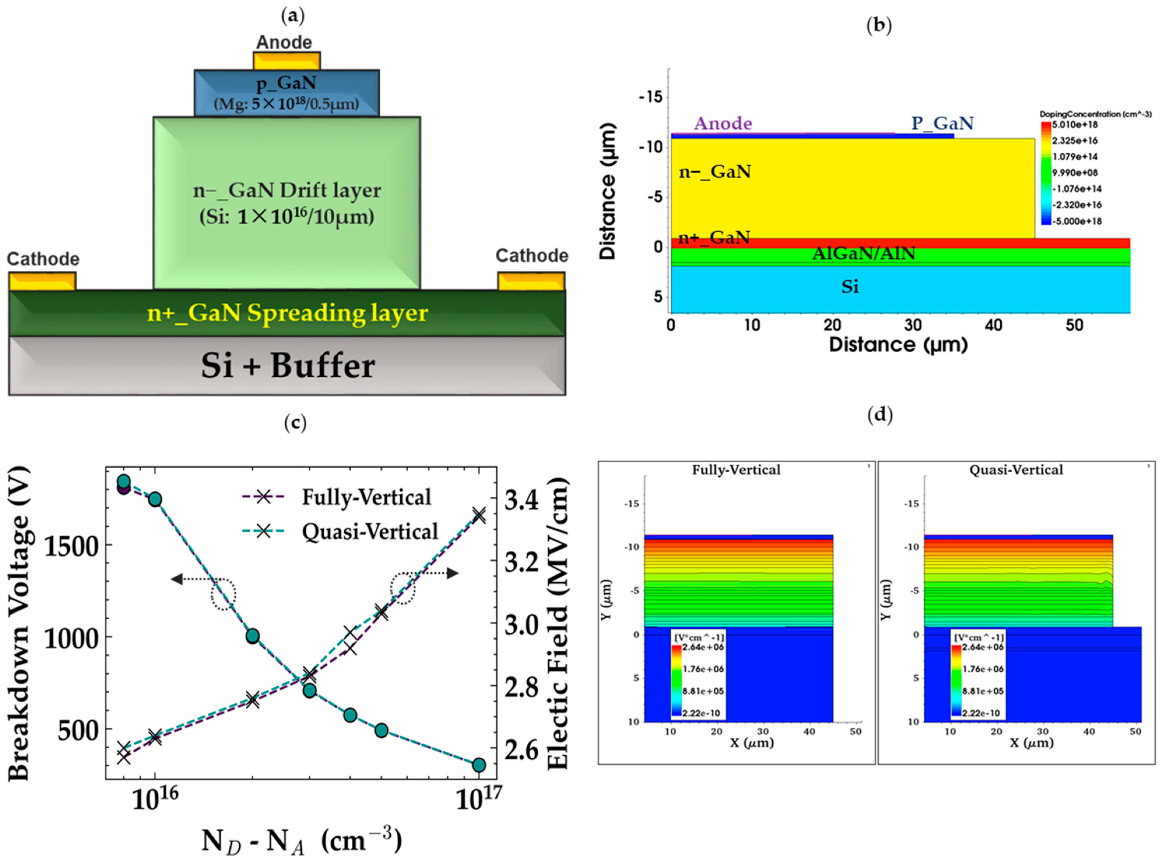
2.1. Prototype Device Structure and Parameters
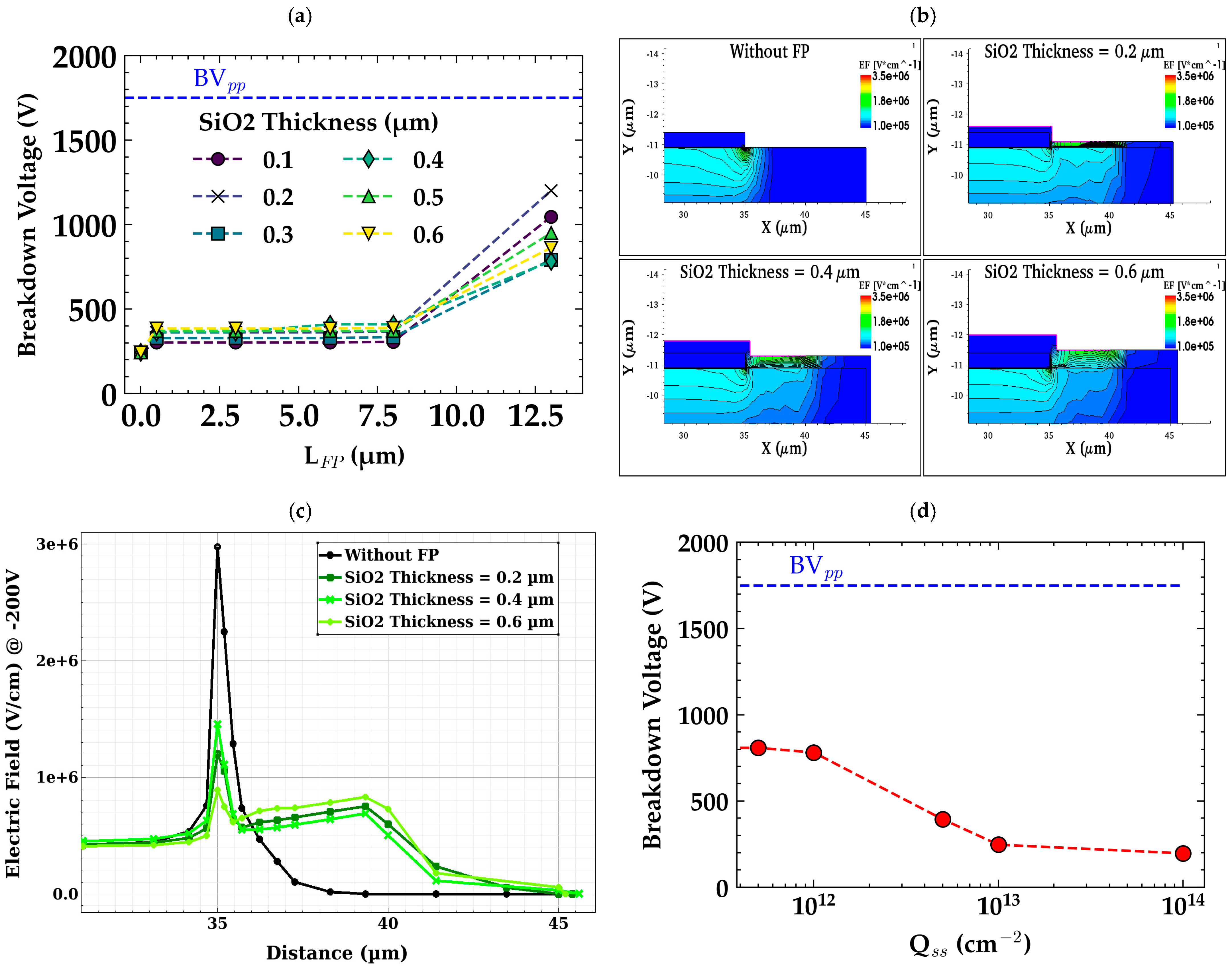
2.2. Metal Field Plates
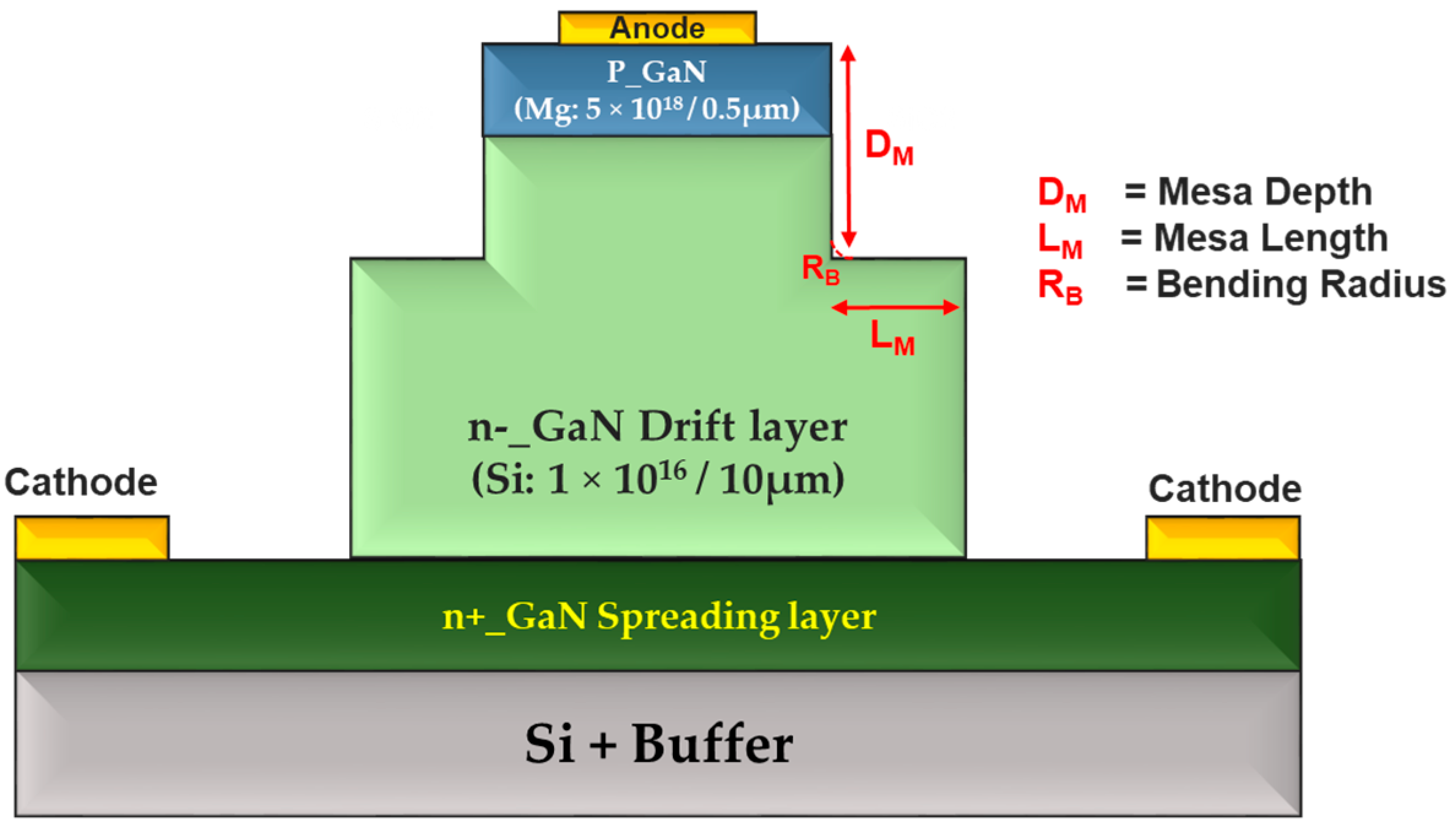
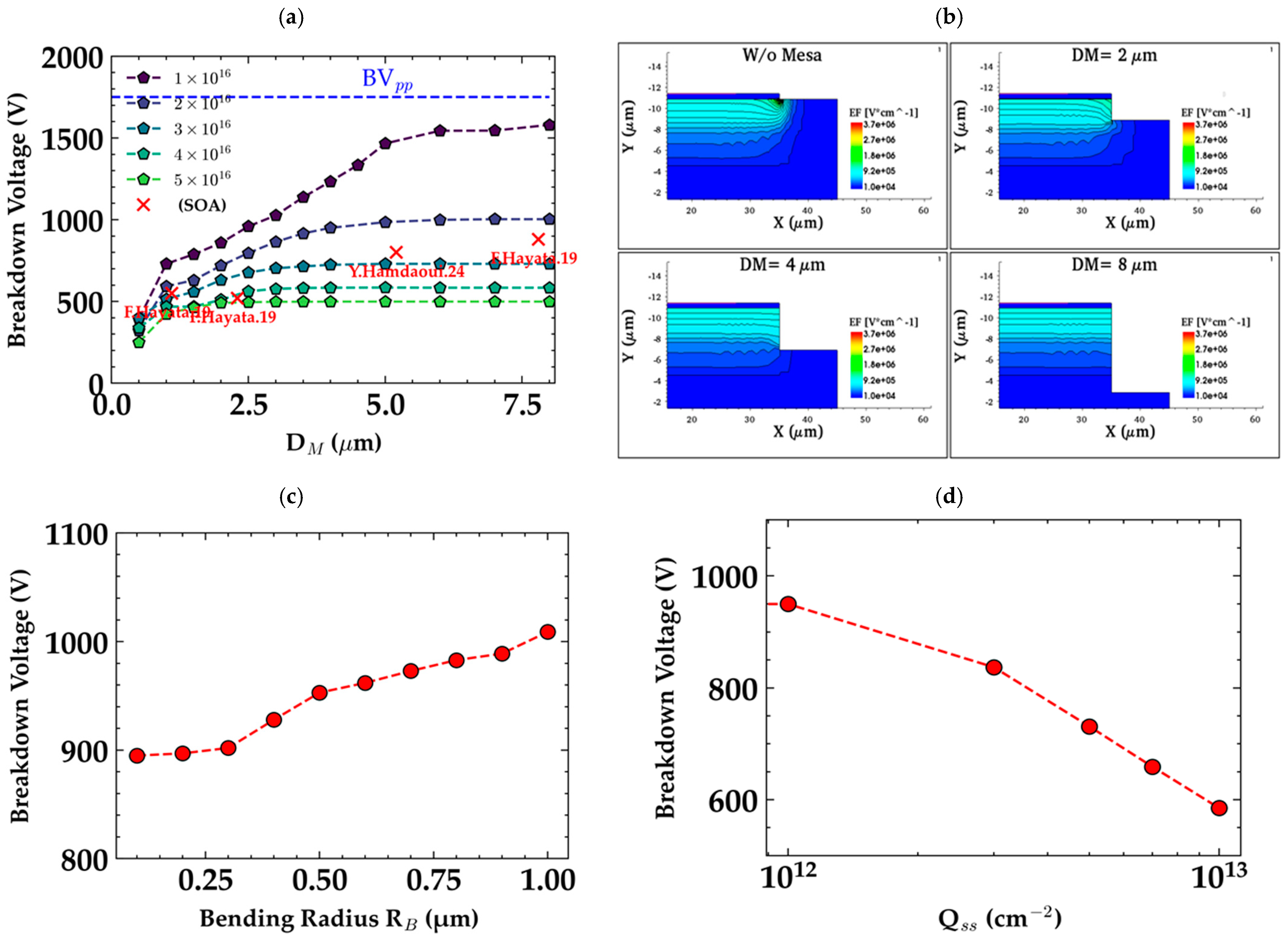
2.3. Mesa
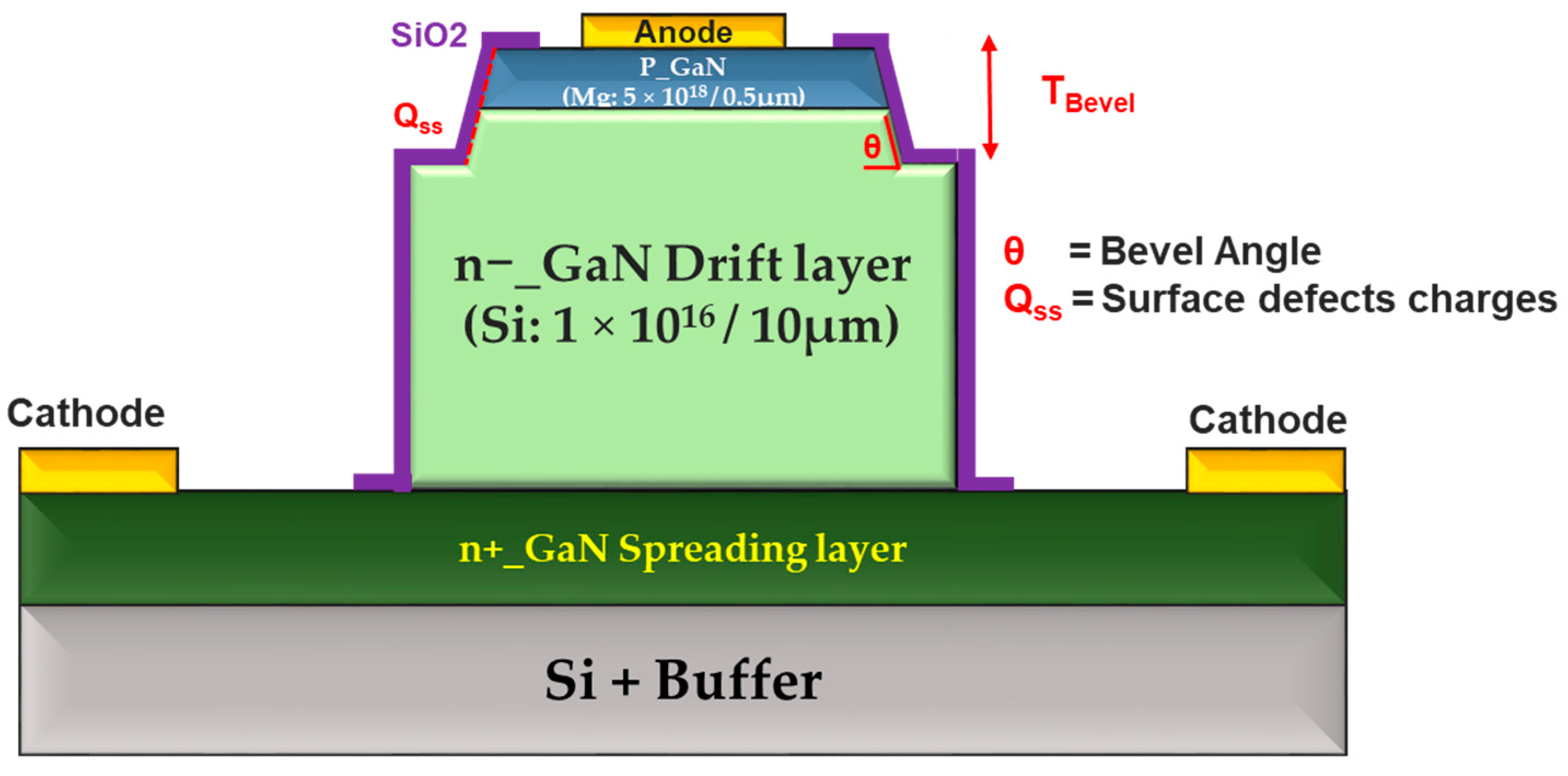
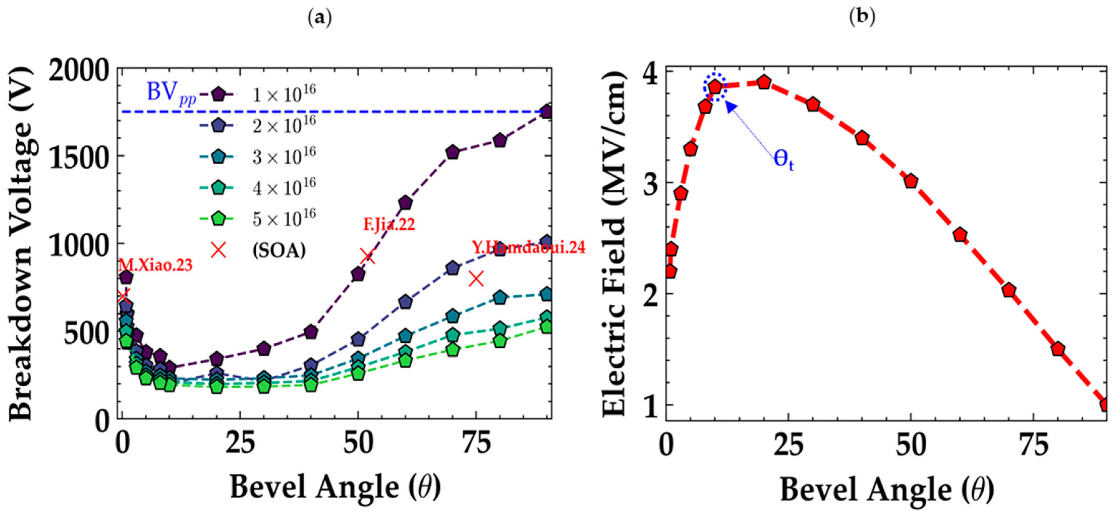
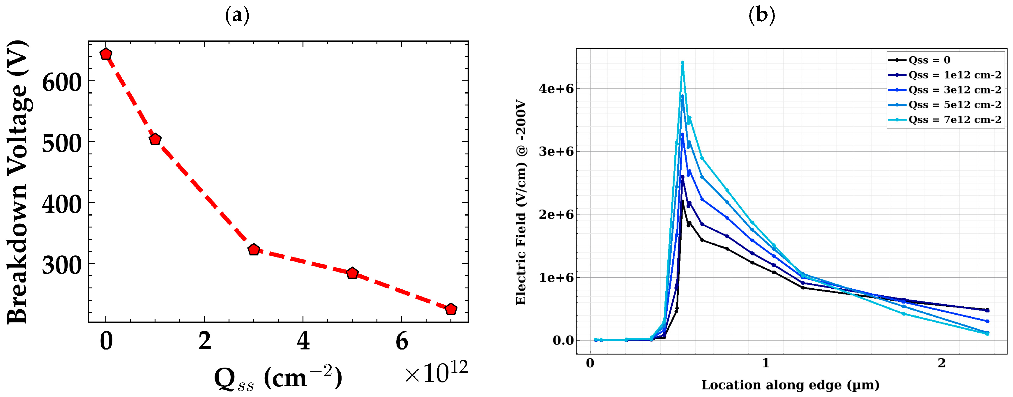
2.4. Bevel Mesa
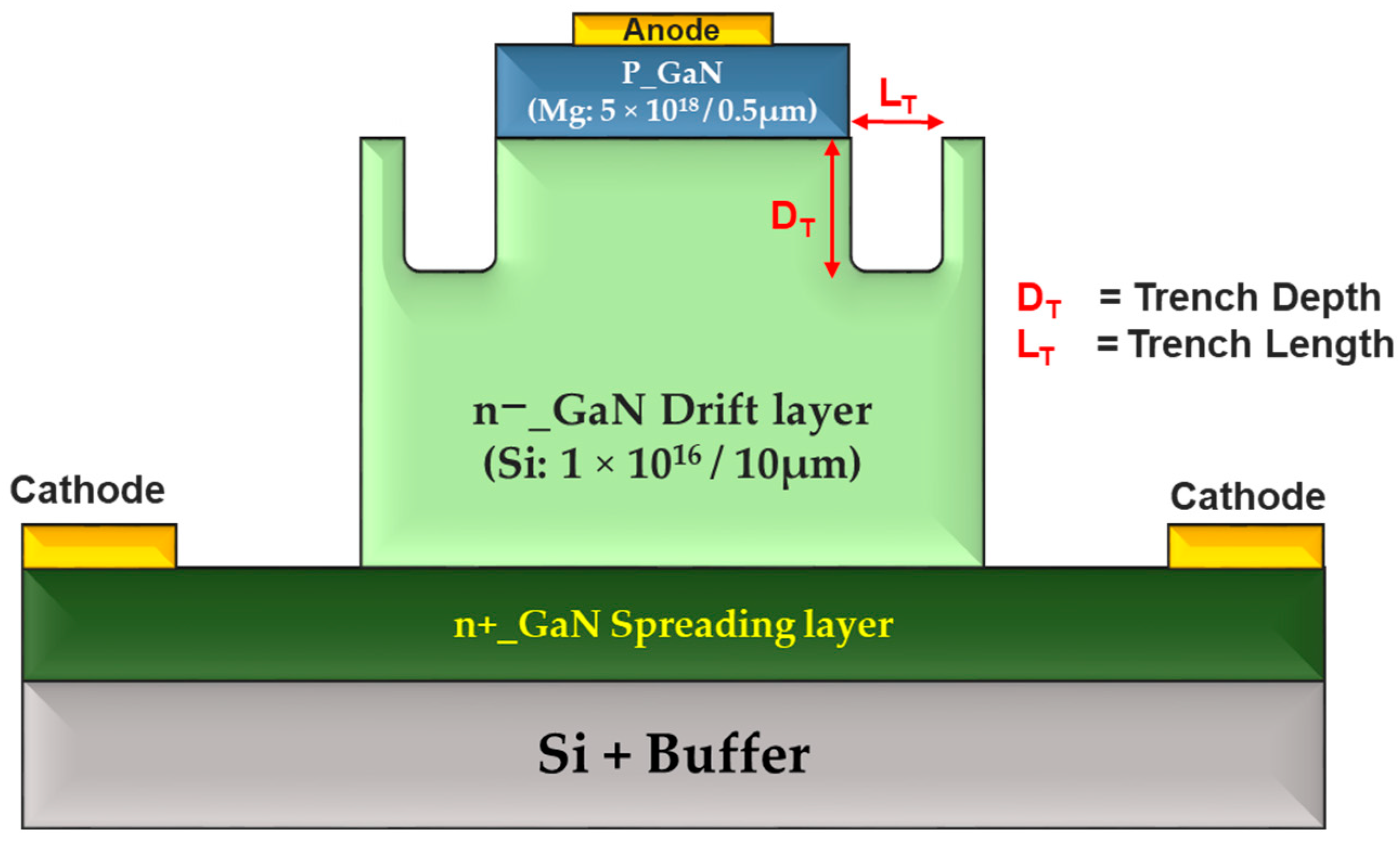
2.5. Trench Termination TT
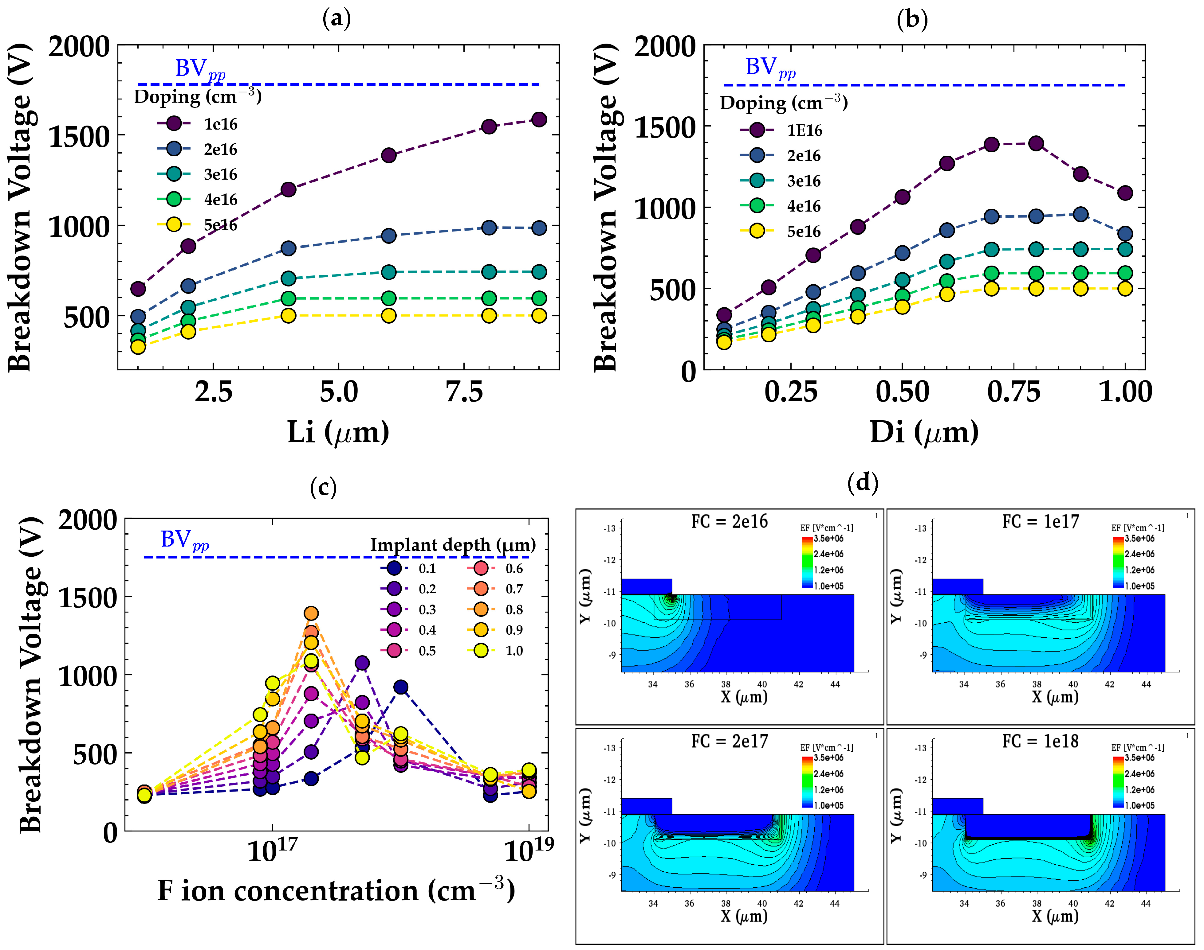
2.6. Ion Implantation
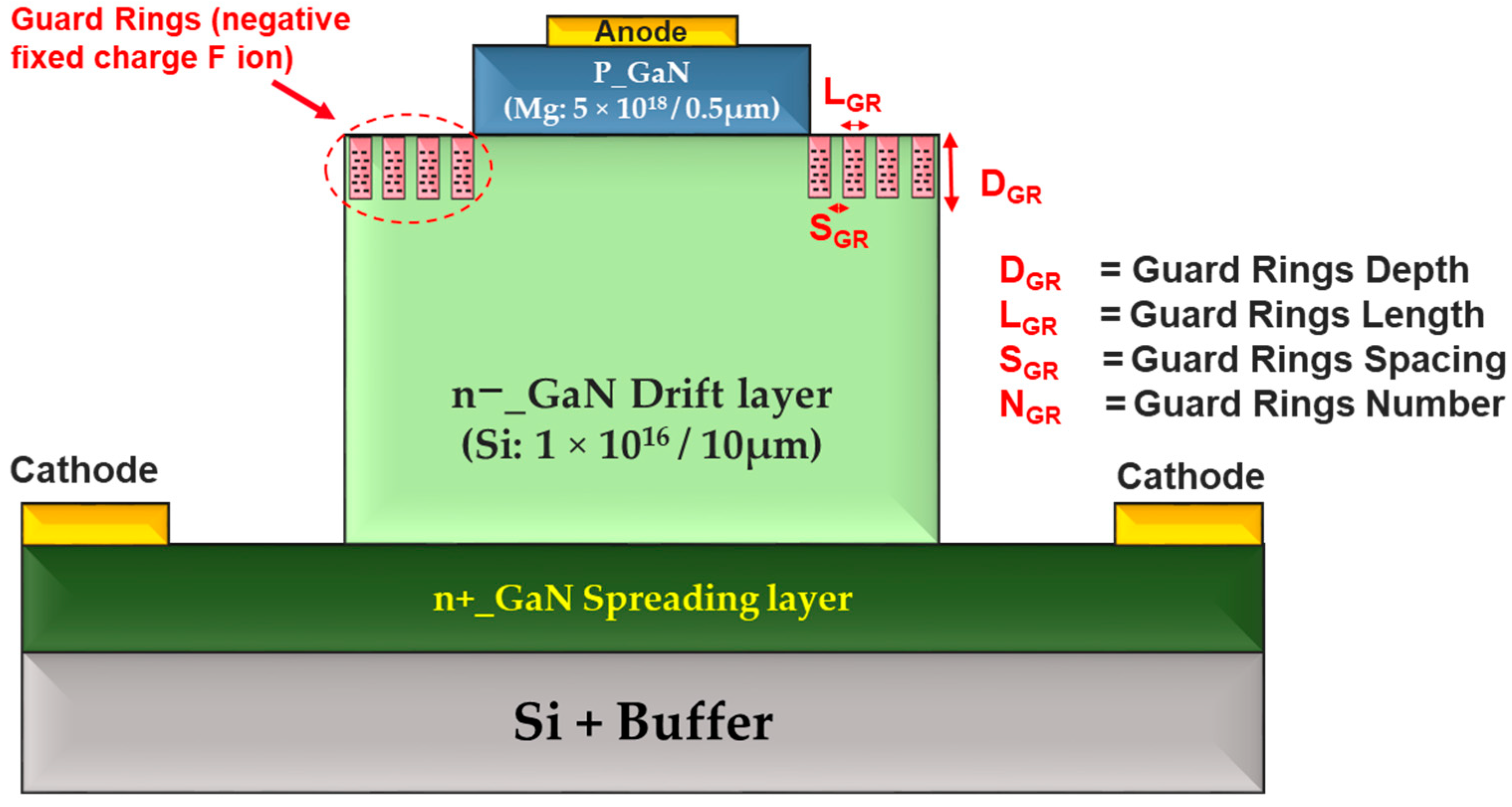
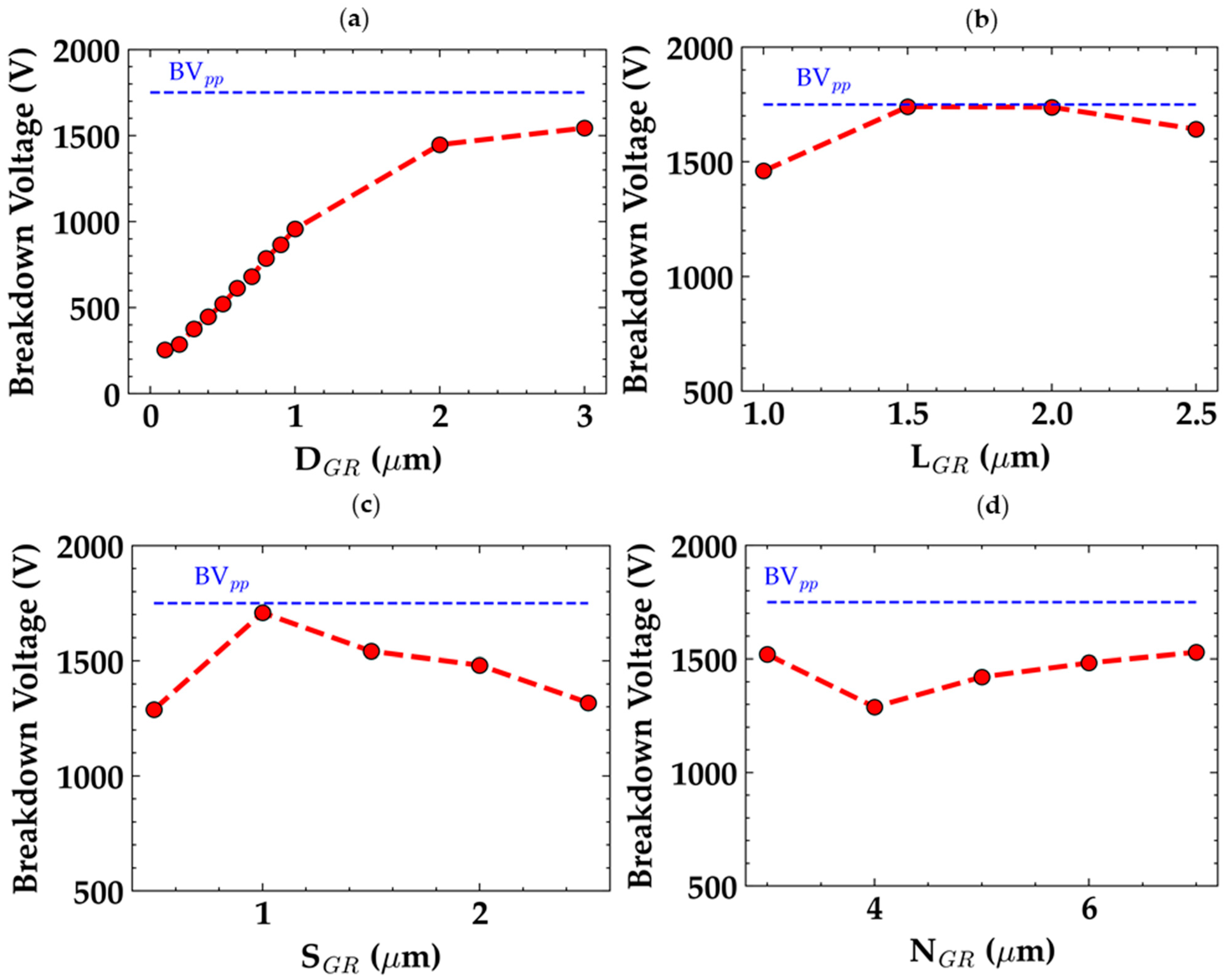
2.7. Guard Rings
3. Conclusions
- (a)
- Field Plate (FP) Termination: This method is highly effective in extending the high-voltage region and smoothing electric field transitions. However, it requires precise metallization steps and careful alignment of the field plates, which can add to the fabrication complexity.
- (b)
- Mesa Termination: Mesa involves creating a stepped surface to direct electric fields away from the device edges. This method is relatively simple to fabricate using standard etching techniques, making it a cost-effective solution for many power devices. Its simplicity, however, may limit its performance in very high-voltage applications compared to other more advanced techniques.
- (c)
- Bevel Termination: Beveling the device edges helps to reduce electric field intensity at the corners, effectively preventing breakdowns. The fabrication of bevel edges requires precise angle control, which can be challenging. Bevel termination offers a good balance between performance and ease of fabrication, making it suitable for medium-voltage applications.
- (d)
- Trench Termination: Trench termination, especially when combined with materials like Benzocyclobutene (BCB), reduces electric field crowding and improves performance. Fabricating trenches with high precision is more complex and requires additional steps like trench filling and planarization, which increases fabrication costs and complexity. However, trench termination excels in high-voltage applications where field control is critical.
- (e)
- Ion Implantation Termination: This method modifies the edge termination with species like fluorine (F), which helps prevent premature breakdown. Ion implantation is a relatively straightforward process compared to trench termination but requires careful control of implantation depth and concentration. While the process is not as complex as trenching or field plating, the optimization of ion concentration and depth for maximum BV performance requires high precision, which can make this method more challenging from a production point of view than simpler techniques like bevel termination.
- (f)
- Guard Ring (GR) Termination: Guard ring termination distributes the electric field evenly around the device. While the concept is simple, optimizing guard ring parameters such as depth, length, spacing, and the number of rings can add fabrication complexity. It requires precise alignment of the guard rings, which increases manufacturing time and cost. However, it is a highly effective technique for high-voltage and high frequency applications, where the benefits in terms of field control justify the added complexity.
Author Contributions
Funding
Data Availability Statement
Acknowledgments
Conflicts of Interest
References
- Fu, H.; Fu, K.; Chowdhury, S.; Palacios, T.; Zhao, Y. Vertical GaN Power Devices: Device Principles and Fabrication Technologies—Part I. IEEE Trans. Electron Devices 2021, 68, 3200–3211. [Google Scholar] [CrossRef]
- Zhang, Y.; Dadgar, A.; Palacios, T. Gallium nitride vertical power devices on foreign substrates: A review and outlook. J. Phys. Appl. Phys. 2018, 51, 273001. [Google Scholar] [CrossRef]
- Langpoklakpam, C.; Liu, A.-C.; Hsiao, Y.-K.; Lin, C.-H.; Kuo, H.-C. Vertical GaN MOSFET Power Devices. Micromachines 2023, 14, 1937. [Google Scholar] [CrossRef] [PubMed]
- Roccaforte, F.; Greco, G.; Fiorenza, P.; Iucolano, F. An Overview of Normally-Off GaN-Based High Electron Mobility Transistors. Materials 2019, 12, 1599. [Google Scholar] [CrossRef] [PubMed]
- Ding, X.; Zhou, Y.; Cheng, J. A review of gallium nitride power device and its applications in motor drive. CES Trans. Electr. Mach. Syst. 2019, 3, 54–64. [Google Scholar] [CrossRef]
- Alquier, D.; Cayrel, F.; Menard, O.; Bazin, A.-E.; Yvon, A.; Collard, E. Recent Progresses in GaN Power Rectifier. Jpn. J. Appl. Phys. 2012, 51, 01AG08. [Google Scholar] [CrossRef]
- Kachi, T. State-of-the-art GaN vertical power devices. In Proceedings of the 2015 IEEE International Electron Devices Meeting (IEDM), Washington, DC, USA, 7–9 December 2015; pp. 16.1.1–16.1.4. [Google Scholar]
- Zhang, Y.; Sun, M.; Piedra, D.; Azize, M.; Zhang, X.; Fujishima, T.; Palacios, T. GaN-on-Si Vertical Schottky and p-n Diodes. IEEE Electron Device Lett. 2014, 35, 618–620. [Google Scholar] [CrossRef]
- Sun, Y.; Kang, X.; Zheng, Y.; Lu, J.; Tian, X.; Wei, K.; Wu, H.; Wang, W.; Liu, X.; Zhang, G. Review of the Recent Progress on GaN-Based Vertical Power Schottky Barrier Diodes (SBDs). Electronics 2019, 8, 575. [Google Scholar] [CrossRef]
- Hatakeyama, Y.; Nomoto, K.; Kaneda, N.; Kawano, T.; Mishima, T.; Nakamura, T. Over 3.0 GW/cm2 Figure-of-Merit GaN p-n Junction Diodes on Free-Standing GaN Substrates. IEEE Electron Device Lett. 2011, 32, 1674–1676. [Google Scholar] [CrossRef]
- Bian, Z.; Zeng, K.; Chowdhury, S. 2.8 kV Avalanche in Vertical GaN PN Diode Utilizing Field Plate on Hydrogen Passivated P-Layer. IEEE Electron Device Lett. 2022, 43, 596–599. [Google Scholar] [CrossRef]
- Kizilyalli, I.C.; Edwards, A.P.; Nie, H.; Bui-Quang, P.; Disney, D.; Bour, D. 400-A (Pulsed) Vertical GaN p-n Diode with Breakdown Voltage of 700 V. IEEE Electron Device Lett. 2014, 35, 654–656. [Google Scholar] [CrossRef]
- Kizilyalli, I.C.; Edwards, A.P.; Nie, H.; Bour, D.; Prunty, T.; Disney, D. 3.7 kV Vertical GaN PN Diodes. IEEE Electron Device Lett. 2014, 35, 247–249. [Google Scholar] [CrossRef]
- Xu, Z.; Detchprohm, T.; Shen, S.-C.; Nepomuk Otte, A.; Dupuis, R.D. Low Leakage and High Gain GaN p-i-n Avalanche Photodiode with Shallow Bevel Mesa Edge Termination and Recessed Window. IEEE Trans. Electron Devices 2024, 71, 3761–3768. [Google Scholar] [CrossRef]
- Lee, S.-H.; Cha, H.-Y. Design of Trench MIS Field Plate Structure for Edge Termination of GaN Vertical PN Diode. Micromachines 2023, 14, 2005. [Google Scholar] [CrossRef] [PubMed]
- Duan, Y.; Wang, J.; Xie, A.; Zhu, Z.; Fay, P. 1.7-kV vertical GaN p-n diode with triple-zone graded junction termination extension formed by ion-implantation. E-Prime—Adv. Electr. Eng. Electron. Energy 2023, 6, 100330. [Google Scholar] [CrossRef]
- Sergei-Ion Implantation in GaN-01.pdf. Available online: https://people.physics.anu.edu.au/~cxj109/Publications/Sergei-Ion%20Implantation%20in%20GaN-01.pdf (accessed on 5 March 2024).
- Fu, K.; He, Z.; Yang, C.; Zhou, J.; Fu, H.; Zhao, Y. GaN-on-GaN p-i-n diodes with avalanche capability enabled by eliminating surface leakage with hydrogen plasma treatment. Appl. Phys. Lett. 2022, 121, 092103. [Google Scholar] [CrossRef]
- Fukushima, H.; Usami, S.; Ogura, M.; Ando, Y.; Tanaka, A.; Deki, M.; Kushimoto, M.; Nitta, S.; Honda, Y.; Amano, H. Vertical GaN p-n diode with deeply etched mesa and capability of avalanche breakdown. Appl. Phys. Express 2019, 12, 026502. [Google Scholar] [CrossRef]
- Shi, S.; Wang, G.; Xiang, Y.; Guo, C.; Wang, X.; Pu, Y.; Li, H.; Li, Z. Investigation on Breakdown Characteristics of Various Surface Terminal Structures for GaN-Based Vertical P-i-N Diodes. J. Appl. Math. Phys. 2024, 12, 554–568. [Google Scholar] [CrossRef]
- Zeng, K.; Chowdhury, S. Designing Beveled Edge Termination in GaN Vertical p-i-n Diode-Bevel Angle, Doping, and Passivation. IEEE Trans. Electron Devices 2020, 67, 2457–2462. [Google Scholar] [CrossRef]
- El Amrani, M.; Buckley, J.; Kaltsounis, T.; Arguello, D.P.; El Rammouz, H.; Alquier, D.; Charles, M. Study of Leakage Current Transport Mechanisms in Pseudo-Vertical GaN-on-Silicon Schottky Diode Grown by Localized Epitaxy. Crystals 2024, 14, 553. [Google Scholar] [CrossRef]
- Yates, L.; Gunning, B.P.; Crawford, M.H.; Steinfeldt, J.; Smith, M.L.; Abate, V.M.; Dickerson, J.R.; Armstrong, A.M.; Binder, A.; Allerman, A.A.; et al. Demonstration of >6.0-kV Breakdown Voltage in Large Area Vertical GaN p-n Diodes with Step-Etched Junction Termination Extensions. IEEE Trans. Electron Devices 2022, 69, 1931–1937. [Google Scholar] [CrossRef]
- Zhang, X.; Zou, X.; Lu, X.; Tang, C.W.; Lau, K.M. Fully- and Quasi-Vertical GaN-on-Si p-i-n Diodes: High Performance and Comprehensive Comparison. IEEE Trans. Electron Devices 2017, 64, 809–815. [Google Scholar] [CrossRef]
- Zhang, Y.; Piedra, D.; Sun, M.; Hennig, J.; Dadgar, A.; Yu, L.; Palacios, T. High-Performance 500 V Quasi- and Fully-Vertical GaN-on-Si pn Diodes. IEEE Electron Device Lett. 2017, 38, 248–251. [Google Scholar] [CrossRef]
- HAL PDF Full Text. Available online: https://hal.science/hal-04436387v1/file/CSW-2023_Abstract_IEMN-Siltronic.pdf (accessed on 19 February 2025).
- Baliga, B.J. Fundamentals of Power Semiconductor Devices; Springer International Publishing: Cham, Switzerland, 2019; ISBN 978-3-319-93987-2. [Google Scholar]
- Maeda, T.; Narita, T.; Yamada, S.; Kachi, T.; Kimoto, T.; Horita, M.; Suda, J. Impact ionization coefficients and critical electric field in GaN. J. Appl. Phys. 2021, 129, 185702. [Google Scholar] [CrossRef]
- Sze, S.M. Physics of Semiconductor Devices, 3rd ed.; Wiley-Interscience: Hoboken, NJ, USA, 2007. [Google Scholar]
- Cao, L.; Wang, J.; Harden, G.; Ye, H.; Stillwell, R.; Hoffman, A.J.; Fay, P. Experimental characterization of impact ionization coefficients for electrons and holes in GaN grown on bulk GaN substrates. Appl. Phys. Lett. 2018, 112, 262103. [Google Scholar] [CrossRef]
- Chung, S.K.; Han, S.Y. Design curves of breakdown voltage at field plate edge and effect of interface charge. Microelectron. J. 2002, 33, 399–402. [Google Scholar] [CrossRef]
- Hatakeyama, Y.; Nomoto, K.; Terano, A.; Kaneda, N.; Tsuchiya, T.; Mishima, T.; Nakamura, T. High-Breakdown-Voltage and Low-Specific-on-Resistance GaN p–n Junction Diodes on Free-Standing GaN Substrates Fabricated Through Low-Damage Field-Plate Process. Jpn. J. Appl. Phys. 2013, 52, 028007. [Google Scholar] [CrossRef]
- Engel-Herbert, R.; Hwang, Y.; Stemmer, S. Comparison of methods to quantify interface trap densities at dielectric/III-V semiconductor interfaces. J. Appl. Phys. 2010, 108, 124101. [Google Scholar] [CrossRef]
- Fukushima, H.; Usami, S.; Ogura, M.; Ando, Y.; Tanaka, A.; Deki, M.; Kushimoto, M.; Nitta, S.; Honda, Y.; Amano, H. Deeply and vertically etched butte structure of vertical GaN p–n diode with avalanche capability. Jpn. J. Appl. Phys. 2019, 58, SCCD25. [Google Scholar] [CrossRef]
- Zhang, Y.; Sun, M.; Liu, Z.; Piedra, D.; Hu, J.; Gao, X.; Palacios, T. Trench formation and corner rounding in vertical GaN power devices. Appl. Phys. Lett. 2017, 110, 193506. [Google Scholar] [CrossRef]
- Baliga, B.J. Advanced Power MOSFET Concepts; Springer: Boston, MA, USA, 2010; ISBN 978-1-4419-5916-4. [Google Scholar]
- Yamada, S.; Sakurai, H.; Osada, Y.; Furuta, K.; Nakamura, T.; Kamimura, R.; Narita, T.; Suda, J.; Kachi, T. Formation of highly vertical trenches with rounded corners via inductively coupled plasma reactive ion etching for vertical GaN power devices. Appl. Phys. Lett. 2021, 118, 102101. [Google Scholar] [CrossRef]
- Nomoto, K.; Hu, Z.; Song, B.; Zhu, M.; Qi, M.; Yan, R.; Protasenko, V.; Imhoff, E.; Kuo, J.; Kaneda, N.; et al. GaN-on-GaN p-n power diodes with 3.48 kV and 0.95 mΩ-cm2: A record high figure-of-merit of 12.8 GW/cm2. In Proceedings of the 2015 IEEE International Electron Devices Meeting (IEDM), Washington, DC, USA, 7–9 December 2015; pp. 9.7.1–9.7.4. [Google Scholar] [CrossRef]
- Shankar, B.; Zeng, K.; Gunning, B.; Martinez, R.P.; Meng, C.; Flicker, J.; Binder, A.; Dickerson, J.R.; Kaplar, R.; Chowdhury, S. Movement of Current Filaments and its Impact on Avalanche Robustness in Vertical GaN P-N diode Under UIS stress. In Proceedings of the 2022 Device Research Conference (DRC), Columbus, OH, USA, 26–29 June 2022; pp. 1–2. [Google Scholar] [CrossRef]
- Shankar, B.; Bian, Z.; Zeng, K.; Meng, C.; Martinez, R.P.; Chowdhury, S.; Gunning, B.; Flicker, J.; Binder, A.; Dickerson, J.R.; et al. Study of Avalanche Behavior in 3 kV GaN Vertical P-N Diode Under UIS Stress for Edge-termination Optimization. In Proceedings of the 2022 IEEE International Reliability Physics Symposium (IRPS), Dallas, TX, USA, 27–31 March 2022; pp. 2B.2-1–2B.2-4. [Google Scholar] [CrossRef]
- Maeda, T.; Narita, T.; Ueda, H.; Kanechika, M.; Uesugi, T.; Kachi, T.; Kimoto, T.; Horita, M.; Suda, J. Design and Fabrication of GaN p-n Junction Diodes with Negative Beveled-Mesa Termination. IEEE Electron Device Lett. 2019, 40, 941–944. [Google Scholar] [CrossRef]
- Hamdaoui, Y.; Michler, S.; Bidaud, A.; Ziouche, K.; Medjdoub, F. 1200-V Fully Vertical GaN-on-Silicon p-i-n Diodes with Avalanche Capability and High On-State Current Above 10 A. IEEE Trans. Electron Devices 2025, 72, 338–343. [Google Scholar] [CrossRef]
- Jia, F.; Ma, X.; Yang, L.; Zhang, X.; Hou, B.; Zhang, M.; Wu, M.; Niu, X.; Du, J.; Liu, S.; et al. 930V and Low-Leakage Current GaN-on-Si Quasi-Vertical PiN Diode with Beveled-Sidewall Treated by Self-Aligned Fluorine Plasma. IEEE Electron Device Lett. 2022, 43, 1400–1403. [Google Scholar] [CrossRef]
- Hamdaoui, Y.; Abid, I.; Michler, S.; Ziouche, K.; Medjdoub, F. Demonstration of avalanche capability in 800 V vertical GaN-on-silicon diodes. Appl. Phys. Express 2023, 17, 016503. [Google Scholar] [CrossRef]
- Xiao, M.; Wang, Y.; Zhang, R.; Song, Q.; Porter, M.; Carlson, E.; Cheng, K.; Ngo, K.; Zhang, Y. Robust Avalanche in 1.7 kV Vertical GaN Diodes with a Single-Implant Bevel Edge Termination. IEEE Electron Device Lett. 2023, 44, 1616–1619. [Google Scholar] [CrossRef]
- Zhang, Y.; Sun, M.; Wong, H.-Y.; Lin, Y.; Srivastava, P.; Hatem, C.; Azize, M.; Piedra, D.; Yu, L.; Sumitomo, T.; et al. Origin and Control of OFF-State Leakage Current in GaN-on-Si Vertical Diodes. IEEE Trans. Electron Devices 2015, 62, 2155–2161. [Google Scholar] [CrossRef]
- Chang, Y.-F.; Liao, C.-L.; Zheng, B.-S.; Liu, J.-Z.; Ho, C.-L.; Hsieh, K.-C.; Wu, M.-C. Using Two-Step Mesa to Prevent the Effects of Sidewall Defects on the GaN p-i-n Diodes. IEEE J. Quantum Electron. 2015, 51, 1–6. [Google Scholar] [CrossRef]
- Yang, Y.; Cao, X.A. Removing plasma-induced sidewall damage in GaN-based light-emitting diodes by annealing and wet chemical treatments. J. Vac. Sci. Technol. B Microelectron. Nanometer Struct. Process. Meas. Phenom. 2009, 27, 2337–2341. [Google Scholar] [CrossRef]
- Krishna, D.V.; Panchal, A.; Sharma, E.; Dalal, S. Trench edge termination in a GaN-based power device. Mater. Today Proc. 2023, 79, 219–222. [Google Scholar] [CrossRef]
- Théolier, L. Conception de Transistor MOS Haute Tension (1200 Volts) Pour l’électronique de Puissance Phdthesis; Université Paul Sabatier—Toulouse III: Toulouse, France, 2008. [Google Scholar]
- Shiu, J.-Y.; Huang, J.-C.; Desmaris, V.; Chang, C.-T.; Lu, C.-Y.; Kumakura, K.; Makimoto, T.; Zirath, H.; Rorsman, N.; Chang, E.Y. Oxygen Ion Implantation Isolation Planar Process for AlGaN/GaN HEMTs. IEEE Electron Device Lett. 2007, 28, 476–478. [Google Scholar] [CrossRef]
- Maurya, V.; Alquier, D.; El Amrani, M.; Charles, M.; Buckley, J. Optimisation of Negative Fixed Charge Based Edge Termination for Vertical GaN Schottky Devices. Micromachines 2024, 15, 719. [Google Scholar] [CrossRef] [PubMed]
- Ozbek, A.M.; Baliga, B.J. Planar Nearly Ideal Edge-Termination Technique for GaN Devices. IEEE Electron Device Lett. 2011, 32, 300–302. [Google Scholar] [CrossRef]
- Ji, D.; Li, S.; Ercan, B.; Ren, C.; Chowdhury, S. Design and Fabrication of Ion-Implanted Moat Etch Termination Resulting in 0.7 m Ω · cm2/1500 V GaN Diodes. IEEE Electron Device Lett. 2020, 41, 264–267. [Google Scholar] [CrossRef]
- Liu, Y.; Yang, S.; Sheng, K. Design and Optimization of Vertical GaN PiN Diodes with Fluorine-Implanted Termination. IEEE J. Electron Devices Soc. 2020, 8, 241–250. [Google Scholar] [CrossRef]
- Ohta, H.; Hayashi, K.; Horikiri, F.; Yoshino, M.; Nakamura, T.; Mishima, T. 5.0 kV breakdown-voltage vertical GaN p–n junction diodes. Jpn. J. Appl. Phys. 2018, 57, 04FG09. [Google Scholar] [CrossRef]
- Fu, H.; Fu, K.; Alugubelli, S.R.; Cheng, C.-Y.; Huang, X.; Chen, H.; Yang, T.-H.; Yang, C.; Zhou, J.; Montes, J.; et al. High Voltage Vertical GaN p-n Diodes With Hydrogen-Plasma Based Guard Rings. IEEE Electron Device Lett. 2020, 41, 127–130. [Google Scholar] [CrossRef]
- Guo, X.; Zhong, Y.; Zhou, Y.; Su, S.; Chen, X.; Yan, S.; Liu, J.; Sun, X.; Sun, Q.; Yang, H. Nitrogen-Implanted Guard Rings for 600-V Quasi-Vertical GaN-on-Si Schottky Barrier Diodes with a BFOM of 0.26 GW/cm2. IEEE Trans. Electron Devices 2021, 68, 5682–5686. [Google Scholar] [CrossRef]
- Wang, Y.; Porter, M.; Xiao, M.; Lu, A.; Yee, N.; Kravchenko, I.; Srijanto, B.; Cheng, K.; Wong, H.Y.; Zhang, Y. Implanted Guard Ring Edge Termination with Avalanche Capability for Vertical GaN Devices. IEEE Trans. Electron Devices 2024, 71, 1481–1487. [Google Scholar] [CrossRef]
- Pu, T.; Younis, U.; Chiu, H.-C.; Xu, K.; Kuo, H.-C.; Liu, X. Review of Recent Progress on Vertical GaN-Based PN Diodes. Nanoscale Res. Lett. 2021, 16, 101. [Google Scholar] [CrossRef]
- Cho, M.; Xu, Z.; Bakhtiary-Noodeh, M.; Detchprohm, T.; Daeumer, M.A.; Yoo, J.-H.; Shao, Q.; Laurence, T.A.; Key, D.; Hashimoto, T.; et al. 1.2-kV Vertical GaN PIN Rectifier with Ion-Implanted Floating Guard Rings. IEEE Trans. Electron Devices 2023, 70, 4578–4583. [Google Scholar] [CrossRef]


| Edge Termination Technique | Operating Mode | Pros | Cons |
|---|---|---|---|
| Field Plate (FP) | Extends the electric field laterally, reducing peak field strength at the junction edge. | Enhances breakdown voltage, reduces surface charging effects, and improves reliability and performance. | Increased device capacitance, added parasitics, more complex design and fabrication. |
| Mesa | Physically etches a mesa structure to define the device’s active area and control field distribution. | Simple and straightforward fabrication, effective for planar device designs. | Surface damage during etching, increased surface leakage current, lower long-term reliability. |
| Bevel | Creates an angled edge to spread electric field lines and reduce field crowding. | Reduces electric field intensity, improves breakdown voltage, and reduces risk of premature breakdown. | Requires precise angle control during etching, complex and delicate manufacturing process. |
| Trench | Etches deep trenches around the active region to modify field distribution and minimize field crowding. | High breakdown voltage, effective electrical isolation, minimizes surface leakage. | High etching complexity, potential for etch-induced lattice damage, added processing steps. |
| Ion Implantation | Introduces dopant or isolation ions to modify electrical properties and reduce surface traps. | Improves stability, reduces leakage currents, and enhances breakdown voltage and reliability. | Requires precise dose and energy control, potential for crystal lattice damage, complex post-implant annealing. |
| Guard Rings | Uses multiple concentric rings to distribute and control electric field lines at the device periphery. | Simple design, effectively reduces peak electric field intensity, and minimizes leakage. | Increases device footprint, requires additional lithography steps, more complex alignment needed. |
| Physical Phenomenon | Models | Parameters | Values |
|---|---|---|---|
| GaN bandgap | Temperature-dependent bandgap model (@0K) | Bandgap (Eg0) | 3.44 eV |
| Electron affinity (Chi0) | 4.1 eV | ||
| Incomplete ionization | Magnesium (p-doped) | Acceptor activation energy | 200 meV |
| Mobility | Low-field doping-dependent Arora model | µmin | 1500 cm2/Vs |
| µmax | 160 cm2/Vs | ||
| Reference doping | 3 × 1017 cm−3 | ||
| Impact ionization | Electron impact ionization coefficients | an | 4.48 × 108 cm−1 |
| bn | 3.39 × 107 cm−1 | ||
| Hole impact ionization coefficients | ap | 7.13 × 106 cm−1 | |
| bp | 1.46 × 107 cm−1 | ||
| Radiative recombination | Radiative recombination constant | Crad | 1.1 × 10⁻¹⁰ cm3 s−1 |
| Auger recombination | Electron coefficient | An | 3 × 10⁻³¹ cm6 s−1 |
| Hole coefficient | Ap | 3×10⁻³¹ cm6 s−1 |
| Edge Termination | Maximum BV | Complexity | Cost |
|---|---|---|---|
| Field Plate | 1200 | + | + |
| Mesa | 1605 | + | + |
| Bevel | 1570 | ++ | + |
| Trench | 1602 | +++ | ++ |
| Ion Implantation | 1410 | ++ | ++ |
| Guard Ring (GR) | 1740 | +++ | ++ |
Disclaimer/Publisher’s Note: The statements, opinions and data contained in all publications are solely those of the individual author(s) and contributor(s) and not of MDPI and/or the editor(s). MDPI and/or the editor(s) disclaim responsibility for any injury to people or property resulting from any ideas, methods, instructions or products referred to in the content. |
© 2025 by the authors. Licensee MDPI, Basel, Switzerland. This article is an open access article distributed under the terms and conditions of the Creative Commons Attribution (CC BY) license (https://creativecommons.org/licenses/by/4.0/).
Share and Cite
El Amrani, M.; Buckley, J.; Alquier, D.; Godignon, P.; Charles, M. Analysis of Edge Termination Techniques for Gallium Nitride Pseudo-Vertical p-n Diodes: Modeling Based on Technology Computer-Aided Design and Review of Current Developments. Electronics 2025, 14, 1188. https://doi.org/10.3390/electronics14061188
El Amrani M, Buckley J, Alquier D, Godignon P, Charles M. Analysis of Edge Termination Techniques for Gallium Nitride Pseudo-Vertical p-n Diodes: Modeling Based on Technology Computer-Aided Design and Review of Current Developments. Electronics. 2025; 14(6):1188. https://doi.org/10.3390/electronics14061188
Chicago/Turabian StyleEl Amrani, Mohammed, Julien Buckley, Daniel Alquier, Philippe Godignon, and Matthew Charles. 2025. "Analysis of Edge Termination Techniques for Gallium Nitride Pseudo-Vertical p-n Diodes: Modeling Based on Technology Computer-Aided Design and Review of Current Developments" Electronics 14, no. 6: 1188. https://doi.org/10.3390/electronics14061188
APA StyleEl Amrani, M., Buckley, J., Alquier, D., Godignon, P., & Charles, M. (2025). Analysis of Edge Termination Techniques for Gallium Nitride Pseudo-Vertical p-n Diodes: Modeling Based on Technology Computer-Aided Design and Review of Current Developments. Electronics, 14(6), 1188. https://doi.org/10.3390/electronics14061188