Article

Heuristic Enz–Krummenacher–Vittoz (EKV) Model Fitting for Low-Power Integrated Circuit Design: An Open-Source Implementation

Dipartimento di Ingegneria dell’Informazione, University of Pisa, 56122 Pisa, Italy
Electronics 2025, 14(6), 1162; https://doi.org/10.3390/electronics14061162
Submission received: 7 January 2025 / Revised: 10 March 2025 / Accepted: 14 March 2025 / Published: 16 March 2025

Abstract

:
Accurate parameter extraction for the Enz–Krummenacher–Vittoz (EKV) model is crucial for low-power integrated circuit design, especially in weak and moderate inversion regions. This work introduces a novel iterative subranging (ISR) technique for EKV model fitting, implemented in Python (version 3.10.12) using SciPy (version 1.10.1), NumPy (version 1.24.3), and Matplotlib (version 3.7.1). The core of the methodology is the Fitter class, which refines the threshold voltage ( V T H ) by progressively narrowing the fitting range, controlled by the fit_range_parameter. This approach achieves a relative fitting error below 5% within a continuous interval of drain current, ensuring accurate parameter extraction in the region of interest while considering the full data range. Validation using SkyWater130 NMOS data demonstrated that the ISR method covers an inversion coefficient (IC) range from 1 × 10 3 to nearly 50, showcasing its ability to accurately model device behavior across weak, moderate, and strong inversion. Compared to state-of-the-art EKV extraction methods, the ISR method exhibited at least a ×2 reduction in fitting error within the weak inversion region. More importantly, the ISR method is easily tunable by the designer in order to focus on specific current regions, where a greater accuracy is desired. This is a distinctive characteristic of the ISR method not present in any other extraction procedure. Moreover, the method demonstrated strong robustness against measurement noise, maintaining accuracy even with a 1 nA RMS noise level. This work provides a powerful and accessible tool for EKV model parameter extraction, enhancing reproducibility and accuracy in analog circuit design for low-power applications.

1. Introduction

Effective circuit design necessitates a balance between model accuracy and design tractability. While complex models like BSIM offer high accuracy [1,2,3], their computational complexity can hinder intuitive design exploration and rapid prototyping. Simplified models, such as the classic Schichman–Hodges model [4], provide ease of use but often lack the precision required for modern low-power integrated circuits (ICs), particularly in weak and subthreshold regions of operation. This gap between oversimplified and computationally intensive models poses a significant challenge for designers balancing accuracy and efficiency.
The Enz–Krummenacher–Vittoz (EKV) model emerges as a promising solution [5,6,7]. It achieves a balance between accuracy and simplicity, enabling designers to perform insightful “back-of-the-envelope” calculations and gain deeper physical insights into circuit behavior [8]. By supporting hand calculations and rapid estimations, the EKV model empowers designers to explore design alternatives and refine concepts before resorting to computationally intensive simulations. Thanks to these characteristics, the EKV model attracted significant attention in the low-power-design community. Its use has been demonstrated in various applications, including low-power amplifiers, data converters, and other analog circuits [9,10,11].
This work introduces a novel methodology for efficient EKV model parameter extraction, specifically tailored for low-power IC design. Leveraging open-source tools and a carefully designed fitting algorithm, this approach bridges the gap between analytical insights and simulation-based verification. As part of this work, we have developed freely accessible Python scripts. The use of open-source tools not only enhances accessibility but also promotes reproducibility and collaboration, which are critical for advancing low-power IC design.
The proposed methodology includes considerations on data preprocessing techniques, iterative parameter refinement strategies, and optimizations for low-power applications. Its effectiveness is demonstrated through a case study involving a 1.8 V NFET device from the open-source SkyWater130 technology. The results highlight the accuracy and efficiency of the extraction approach, while also identifying areas for future improvement.
The remainder of this paper is organized as follows: Section 2 provides a brief overview of the MOSFET models with a focus on the EKV model and its relevance to low-power IC design. Section 3 details the proposed heuristic methodology for extracting of the main DC parameters of the MOSFET device, including data preprocessing and parameter refinement strategies. The term heuristic refers to the fit_range_parameter, a dimensionless parameter used in the proposed iterative subranging fitting procedure. Determining the optimal fit_range_parameter for specific voltage and current ranges is not possible a priori, as it depends on the specific transistor characteristics. Section 4 presents the implementation using open-source tools. Section 5 demonstrates the methodology through a case study using the SkyWater130 technology. Finally, Section 6 discusses the results, limitations, and potential future work.

2. Background

2.1. Overview on MOSFET Models

MOSFET modeling is often regarded as an “art” due to the multitude of interacting physical phenomena that define the electrical characteristics of the device. The continuous advancement of FET technologies—including feature downscaling, the introduction of novel materials, and complex geometries beyond traditional epitaxial fabrication—poses significant challenges to the accuracy of established models. This is reflected in the extensive and continually expanding literature on the subject [12,13,14,15,16,17,18,19].
In extremely downscaled MOSFETs found in advanced integrated circuit nodes, several key physical phenomena become prominent. These include short-channel effects (SCEs), such as threshold voltage roll-off and drain-induced barrier lowering (DIBL), where the drain voltage significantly influences the channel potential [12]. Additionally, velocity saturation becomes critical as, at high electric fields, carrier velocity saturates, deviating from the linear relationship with the electric field. Gate-induced drain leakage (GIDL), caused by quantum mechanical tunneling through the gate oxide, and other quantum effects, such as quantum confinement, become increasingly significant as device dimensions shrink [13].
The relative importance of these phenomena in design depends on the specific application. For example, in high-power or RF circuits, velocity saturation may play a crucial role in limiting performance [11], while in ultra-low-power designs, threshold voltage control is paramount. Even small variations in threshold voltage can significantly impact leakage currents and standby power consumption.
In this rapidly evolving landscape, designers heavily rely on the accuracy of device models provided by the technology process design kit (PDK). Industrial standards primarily utilize BSIM (Berkeley Short-channel IGFET Model) [15,16] and HiSIM (Hiroshima University STARC IGFET Model) [17,18], with the PSP (Philips Surface Potential) model also used in some contexts [19]. These surface-potential-based models provide accurate representations of device behavior across a wide range of operating conditions. They incorporate hundreds of parameters to enable precise simulations across varying device dimensions (W and L), process–temperature–voltage (PVT) variations, local mismatch effects, and well-proximity effects. Their standardization ensures compatibility between different EDA tools and foundries, facilitating widespread adoption.
However, the complexity of these models can hinder design intuition and awareness. Therefore, simplified models with a reduced set of parameters are crucial for initial design exploration. These models allow designers to quickly identify promising operating regions before fine-tuning their designs with accurate simulations using the full PDK models.
The square-law model, valid only in strong inversion, provides a basic quadratic relationship between drain current and gate voltage [4], while the exponential model captures subthreshold behavior with a simple exponential dependence. Although useful for fundamental understanding, these models are limited in accuracy and range of validity. Charge-based models, such as EKV (Enz–Krummenacher–Vittoz) [5] and ACM (Advanced Compact MOSFET) [20], introduce the concept of an inversion coefficient (IC) as a key design parameter, replacing the traditional overdrive voltage ( V G S V T H ). This approach facilitates intuitive modeling of moderate and weak inversion regions, going beyond the simple on/off view of device operation.
The inversion coefficient (IC) is defined as a normalized measure of the inversion charge in the channel, capturing the transition between subthreshold, moderate inversion, and strong inversion regions. Unlike the classical overdrive voltage, which does not directly capture the underlying physical mechanisms governing MOSFET operation—especially in the mixed drift–diffusion current regime—IC provides a direct link between the charge-based physics and the MOSFET current conduction mechanisms.
A key advantage of the IC approach is its direct applicability to analog and low-power design. One of the most critical design metrics in analog circuits is the transconductance-to-current ratio ( g m / I D ). This ratio is of great importance, since it is used to quantify the transconductance for a given amount of current (i.e., power consumption). Since g m is pivotal in determining speed, gain, and noise in a vast class of analog circuits [21], the g m / I D ratio is the key parameter to determine power efficiency [22]. Traditional MOSFET models express g m as a function of V G S and V T H , but this approach fails to capture the strong variation in g m / I D in different regions of operation. By contrast, IC-based models naturally express g m / I D as a function of IC, providing a single, unified expression valid across all operating regions [23]:
g m I D = 1 n U T · 1 e IC IC ,
where n is the subthreshold slope factor and U T = k B T / q is the thermal voltage (here, k B is the Boltzmann constant, T the operating temperature, and q the elementary charge). Equation (1) predicts the saturation of the g m / I D ratio to a maximum value of 1 / ( n U T ) in weak inversion (small values of IC). Conversely, in strong inversion (where IC is significantly larger than unity), it predicts a 1 / IC roll-off, indicating a decrease in transconductance efficiency with increasing inversion charge.
While both the EKV and ACM models share the fundamental concept of the inversion coefficient, they differ in their mathematical formulations and application contexts. The EKV model, known for its simplicity, symmetry, and analytical tractability, is particularly well suited for hand calculations and educational purposes. It provides a clear and unified understanding of MOSFET behavior across all regions of operation (weak, moderate, and strong inversion) and emphasizes normalized currents, making it intuitive for analog design. In contrast, the ACM model focuses on higher accuracy and incorporates more detailed physical effects, such as mobility degradation, velocity saturation, and short-channel effects, making it suitable for computer-aided design and simulation of deep-submicron and nanometer-scale technologies [24]. While the EKV model is ideal for initial design exploration and gaining physical insight, the ACM model is better equipped for detailed, technology-specific simulations. Therefore, the two models are not strictly competing but rather complementary, each serving different needs in the design and analysis of MOSFETs.
While the EKV model offers greater detail and accuracy compared to oversimplified models, the challenge of extracting accurate model parameters from electrical measurements remains. As previously discussed, various physical phenomena can limit the accuracy of the EKV model. From a device modeling perspective, several strategies have been employed to enhance accuracy. These include explicitly introducing new parameters into the current equations, such as the channel length modulation parameter λ , and incorporating implicit dependencies in the main parameters, like the voltage dependence of the subthreshold slope factor. Adaptations of the EKV model, tailored for accurate electrical simulation, have emerged, employing a comprehensive set of parameters to reflect the physical effects previously outlined [25].
While these approaches enhance model fidelity, they increase complexity, potentially hindering the designer’s practical use of the model. In contrast, this work adopts a different approach: maintaining minimal model complexity while defining a clear region of validity in terms of voltage and current ranges. This strategy promotes greater confidence and awareness of the model’s local accuracy in design practice, facilitating its effective application.
While numerous parameter extraction methodologies have been proposed in the literature [26,27,28], this work distinguishes itself by addressing a critical limitation found in existing approaches. Notably, a recent parameter extraction procedure from Enz’s group [8] shares similarities with conventional MOSFET parameter extraction, particularly in its initial electrical test bench setup. This method, which will serve as a comparative benchmark in Section 5, provides global estimations of MOSFET parameters across the entire range of electrical characteristics. However, it lacks the ability to prioritize accuracy within specific operating regions.
In contrast, the novel contribution of this work lies in its development of a parameter extraction methodology that maintains simplicity while introducing a mechanism to adapt fitting accuracy to targeted MOSFET operating regions, spanning from weak to strong inversion. This allows designers to tailor the model precision to their specific application requirements, ensuring accurate representations of device behavior within critical operating regimes. This is achieved by the introduction of a specific parameter to control the fitting range. The role of this new parameter, termed fit_range_parameter, is extensively discussed in Section 3.3.

2.2. The Simplified EKV Model

In the simplified EKV model [5,8], the drain current I D is a function of voltage applied to the gate, the source, the drain, and the bulk terminals. The latter is usually used as local reference; hence, the following potentials are considered: V G B , V S B , and V D B , corresponding, respectively, to the gate–bulk voltage, the source–bulk voltage, and the drain–bulk voltage. The EKV expression for I D is as follows:
I D = I S ln 2 1 + exp V P V S B 2 U T ln 2 1 + exp V P V D B 2 U T ,
where
  • I S is the specific current, given by I S = 2 n μ C o x U T 2 W L ;
  • V P is the pinch-off voltage, defined as V P = V G B V T H n (here, V T H is typically defined as the gate voltage at which the inversion charge density equals the depletion charge density);
  • U T and n are the thermal voltage and the subthreshold slope factor, respectively (previously defined in Section 2.1);
  • μ is the carrier mobility;
  • C o x is the oxide capacitance per unit area;
  • W and L are the width and the length of the transistor, respectively.
Starting from Equation (2), approximate forms can be derived considering, for example, the saturation region ( V D B V p ): I D I S ln 2 1 + exp V P V S B 2 U T . On the other hand, further approximations can be derived for weak inversion (w.i.) or strong inversion (s.i.) operation, which are usually the basis of hand calculations:
I D I S exp V G B V T H n U T exp V S B U T ( w . i . ) ;
I D β 2 n V G B V T H n V S B 2 , where β = I S 2 n U T 2 ( s . i . ) .
The inversion coefficient, IC, is defined as follows:
IC = I D I S .
As already discussed, IC is a common indicator for the region of operation: IC < 0.1 indicates w.i. operation, 0.1 < IC < 10 indicates moderate inversion (m.i.), and, finally, IC > 10 indicates s.i. operation. A complete derivation of approximate expressions can be found in [29].

2.3. The Rise of Open-Source Tools in Integrated Circuit Design

The increasing adoption of open-source tools and methodologies has significantly impacted the landscape of integrated circuit design. Open-source tools offer several key advantages:
  • Accessibility: Open-source tools are freely available, democratizing access to advanced design tools and empowering researchers, academics, and independent designers [30].
  • Cost-Effectiveness: Eliminating the high costs associated with commercial licenses makes open-source tools an attractive option for both individual researchers and smaller organizations.
  • Transparency and Collaboration: Open-source tools foster transparency and collaboration by allowing users to inspect, modify, and contribute to the codebase. This collaborative environment accelerates innovation and fosters a vibrant community of developers and users [31].
  • Security: Open-source tools benefit from a large and active community of developers and users who continuously review and improve the codebase. This collaborative approach enhances security by enabling rapid identification and resolution of vulnerabilities [32,33].
  • Flexibility and Customization: Open-source tools provide greater flexibility and customization options compared to commercial tools, allowing users to tailor them to their specific needs and research requirements [34,35].
  • Education and Research: Open-source tools play a crucial role in education and research by providing students and researchers with hands-on experience with real-world design tools and methodologies [36].
The growing maturity and capabilities of open-source EDA tools, such as ngspice, GHDL, Verilator, and OpenLane, have made them increasingly viable for academic and industrial applications. These tools provide a powerful platform for design exploration, simulation, and verification, enabling researchers and designers to tackle complex challenges and push the boundaries of integrated circuit technology.
This work leverages the power of open-source tools, developed in the widespread Python language, to develop a readily accessible and customizable framework for EKV model parameter extraction, contributing to the ongoing advancement of open-source EDA and empowering the design community with efficient and accessible tools for low-power circuit design.

3. Methodology

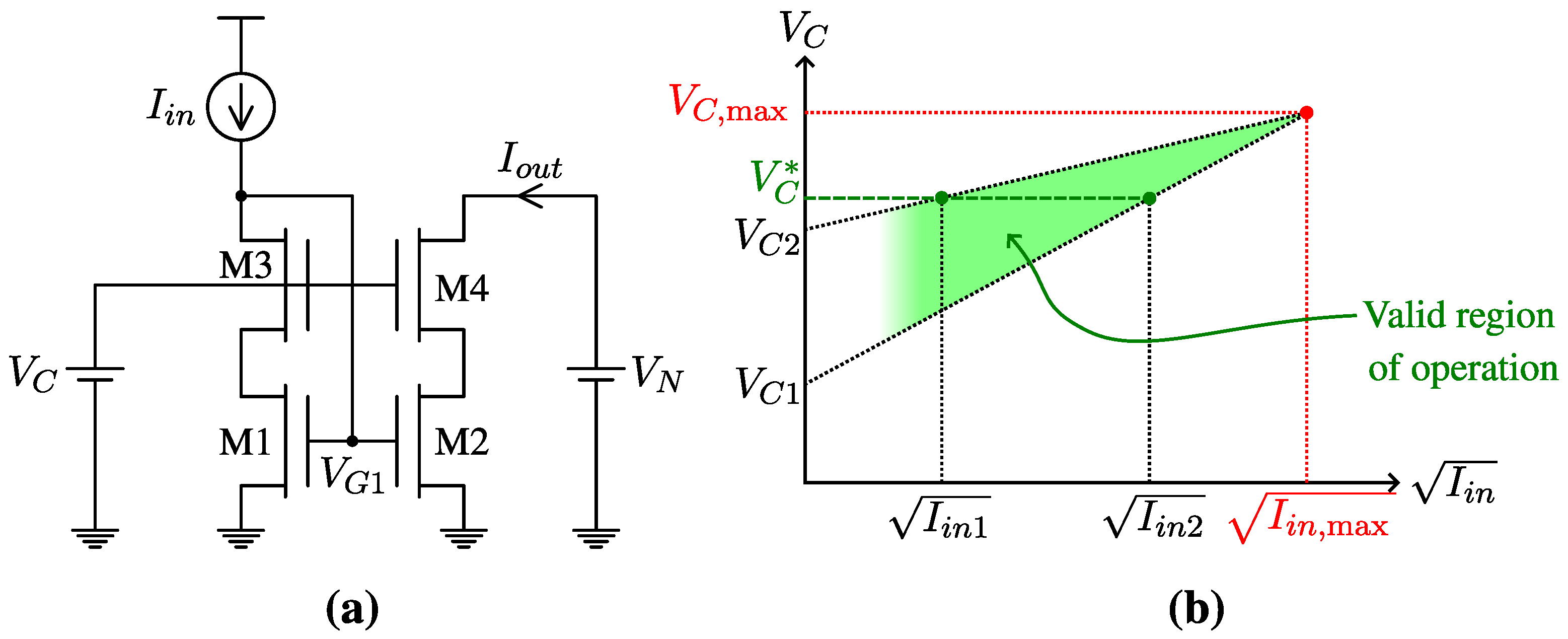
3.1. Electrical Configuration for Data Extraction

This work employs a heuristic approach to extract EKV model parameters from measured I-V characteristics of a generic MOSFET device. The electrical test bench to extract the characteristics of the drain current versus the gate voltage is shown in Figure 1. In this configuration, the bulk and the source terminals are grounded. In this study, the drain voltage was set to 1.2 V to minimize short-channel effects such as DIBL, velocity saturation, and channel length modulation, which are not explicitly included in the current fitting methodology. On the other hand, the value of 1.2 V is high enough to allow saturation operation of the device. While the approach is primarily designed for long-channel MOSFETs, future work will extend the method to incorporate these effects and explore model accuracy under varying drain biases. This configuration is easily reproducible in experimental settings using a two-channel source monitoring unit (SMU).
With this electrical configuration, Equation (2) simplifies to the following:
I D ( V G ) = I S ln 2 1 + exp V G V T H 2 n U T .
The purpose of the fitting is to evaluate the following parameters: V T H , I S , and n.
The extracted I D values are expected to be monotonic with respect to V G and span multiple orders of magnitude (e.g., from femtoamperes to fractions of milliamperes). In real measurement settings, noise may disrupt the monotonic behavior especially at low levels of current. These aspects are relevant to data preprocessing strategies for the fitting procedure.

3.2. Least-Squares Optimization: Weighting and Log-Scaling

In least-squares optimization, the goal is to minimize the sum of the squared residuals between the observed data and the model predictions. Mathematically, this is expressed as follows:
Minimize : i = 1 N I D , meas ( V G , i ) I D , model ( V G , i ) 2 .
Here, I D , meas ( V G , i ) and I D , model ( V G , i ) are the measured and predicted values of the drain current at the gate voltage V G , i , respectively.
Direct application of the least-squares error to data spanning several orders of magnitude leads to dominance of the fitting to the range of data where larger values are present. The residuals (i.e., the terms I D , meas ( V G , i ) I D , model ( V G , i ) ) are squared, so larger currents contribute disproportionately more to the total error. For example, a residual of 1 µA contributes ( 1 × 10 6 ) 2 = 1 × 10 12 , while a residual of 1 fA contributes ( 1 × 10 15 ) 2 = 1 × 10 30 . For this reason, the direct application of a fitting routine on the whole range leads to a fitted model biased toward accurately describing the strong-inversion region at the expense of the weak inversion region.
To address this issue and achieve a better fit across the entire range of operation (weak, moderate, and strong inversion), one can employ the following strategies: (i) weighted least squares (WLS) and (ii) logarithmic scaling (LogS).
The WLS strategy consists of introducing a weighting function to explicitly control the contribution of each data point to the total error. A natural weighting function candidate could be the squared inverse of the measured current:
Minimize : i = 1 N w i · I D , meas ( V G , i ) I D , model ( V G , i ) 2 ; w i = 1 I D , meas 2 ( V G , i ) .
The WLS reduces the dominance of high-current regions by equalizing the weight of low-current regions. However, WLS could lead to overemphasizing noise, both numerical or physical, in the weak inversion region.
The LogS strategy can be used to transform the current data and model predictions into logarithmic space before performing the least-squares optimization. This effectively equalizes the weights of the residuals across all current levels. The optimization problem becomes the following:
Minimize : i = 1 N log 10 I D , meas ( V G , i ) log 10 I D , model ( V G , i ) 2 .
This method is numerically robust, as the extracted I D values from the electrical test bench in Figure 1 are always positive. In the case of real measurements, precaution should be taken to handle zero or negative current values, which may be present at low-current values due to random noise or offsets in the acquisition instrumentation.

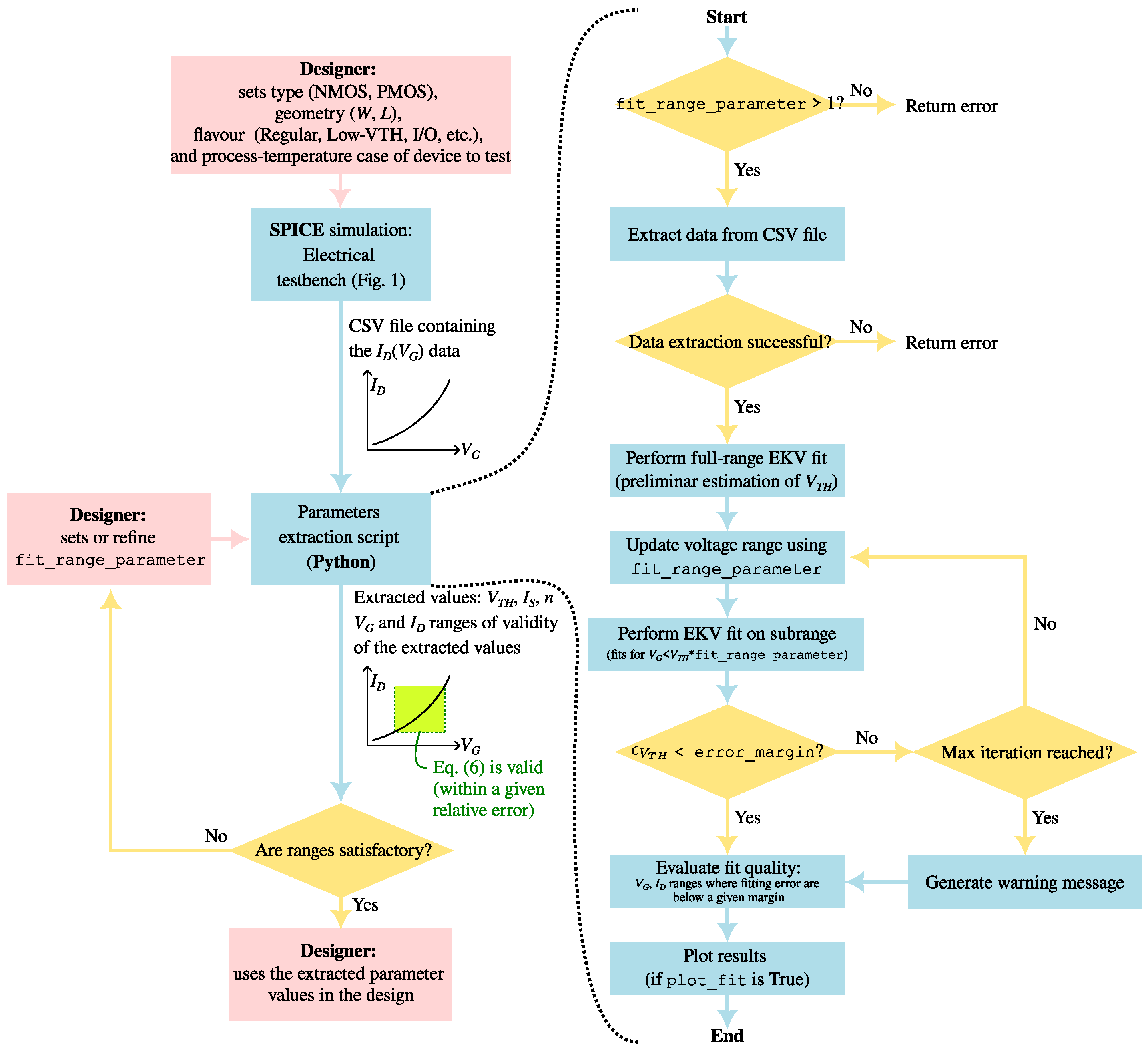
3.3. Heuristic EKV Model Fitting

The core of the methodology lies in an iterative refinement process that focuses on accurately determining the V T H , I S , and n parameters within a specific region of the experimental I D ( V G ) data.
The operative framework of the heuristic EKV fitting method is shown in Figure 2. The designer, after selecting the transistor type (NMOS or PMOS), geometry (W and L), flavor (regular core, low threshold, input/output, etc.), and process/temperature corner conditions, performs a SPICE simulation using the test bench shown in Figure 1. This simulation extracts the I D ( V G ) data, which are then saved to a comma-separated values (CSV) file.
Subsequently, the designer executes the Python script with a trial value for the fit_range_parameter, ranging between 1 and 2. This range will be justified in the following discussion. The script outputs the extracted values of V T H , I S , and n, as well as the region of validity for the fitting of Equation (6) within the I D ( V G ) characteristics. The validity region is determined by evaluating the relative error between the fitted I D and the experimental I D .
If the validity range is unsatisfactory, particularly if the circuit application requires operating values of I D or V G outside this range, the designer can iterate the fitting process with a different fit_range_parameter. As will be discussed later, the fit_range_parameter controls the narrowing of the fitting range.
The value of this parameter influences whether the fitting emphasizes the weak inversion region (low-power operation) or the moderate/strong inversion regions (higher-current conditions). The optimal fit_range_parameter depends on the intended application: smaller values prioritize subthreshold behavior for low-power designs, while larger values are suitable for designs where strong inversion regions are more relevant.
This fitting procedure is termed “heuristic” because the optimal fit_range_parameter is not known a priori, and the designer may iterate the fitting procedure to achieve the desired result. Figure 2 provides an algorithmic overview of the fitting procedure, which consists of three main steps: (i) initial full-range fit; (ii) iterative threshold voltage refinement; and (iii) fit quality assessment. Each step is detailed in the following subsections.

3.3.1. Initial Full-Range Fit

An initial fit is performed across the entire measured voltage range to obtain preliminary estimates for V T H , specific current ( I S ), and subthreshold slope factor (n). The fit is performed using the “curve_fit” function [37] from the SciPy library [38]. The model function is the I D ( V G ) relationship of Equation (6). The initial guess for the three parameters, V T H , I S , and n, is as follows: the average of V G , i , the average of I D ( V G , i ) , and 1.5, respectively.

3.3.2. Iterative Threshold Voltage Refinement

The V G fitting range is progressively narrowed by iteratively reducing the upper voltage bound based on the previously extracted V T H . At each new iteration, the upper bound of the subrange, V G , up , is updated to the following:
V G , up = fit _ range _ parameter · V T H ,
where V T H is the estimated threshold parameter from the previous iteration.
fit_range_parameter controls the extent of this narrowing in each iteration. A value close to 1 emphasizes convergence towards weak inversion behavior, while higher values prioritize stronger inversion regions. In each iteration, the EKV model from Equation (6) is refitted within the reduced voltage range [0, V G , up ], and the new V T H estimate is compared to the previous value.
The iterative process continues until either the relative change in V T H , ϵ V T H , falls below a predefined error margin (given by the error_margin parameter) or the maximum number of iterations is reached. ϵ V T H is calculated from the current and the previous iteration values of V T H , which are V T H ( c ) and V T H ( p ) , respectively, as follows:
ϵ V T H = 2 V T H ( c ) V T H ( p ) V T H ( c ) + V T H ( p ) .
The convergence of this iterative process to the true value of V T H is facilitated by several factors. First, the input I D ( V G ) data are assumed to be monotonic. Second, the fitting relationship defined by Equation (6) is also monotonic. These conditions, while not sufficient, are necessary for convergence given the stopping criterion of Equation (11).
The update rule defined by Equation (10) further enhances convergence by progressively narrowing the fitting region. This effectively reduces the influence of high-end I D values, which could dominate the least-squares error minimization (see Equation (7)) and potentially lead to inaccurate V T H estimates.
Furthermore, within the narrowed fitting region, I D and its derivative with respect to V G are not only monotonic but also exhibit a well-behaved, non-oscillatory trend. This allows for a smooth convergence of the fitting parameters ( V T H , I S , n) without oscillatory or divergent behavior.
To ensure robustness, a maximum iteration limit is implemented as a secondary stopping criterion, safeguarding against potential issues such as incorrect input data that may violate the monotonicity assumptions.
Empirically, the algorithm has demonstrated rapid convergence, with all extraction steps in the case study of Section 5 converging within a maximum of three iterations. This suggests the numerical stability and efficiency of the proposed method.

3.3.3. Fit Quality Assessment

After convergence, the quality of the fit is assessed by comparing the fitted current values to the measured data within a specified voltage range around the final V T H . A quality margin is defined to determine the acceptable deviation between the fitted and measured currents:
I D , meas ( V G , i ) I D , model ( V G , i ) I D , meas ( V G , i ) quality _ margin .
The voltage range within which the fit error remains below the quality margin is identified, providing a measure of the fit validity.

4. Implementation

The proposed methodology is implemented in Python using the following key libraries: NumPy for numerical array operations and mathematical functions; SciPy for curve fitting and optimization algorithms (specifically “curve_fit”); Pandas for efficient data handling and manipulation of the input CSV file; Matplotlib for generating plots to visualize the fitting results.
The core implementation resides in the “_fit_data” method of the “Fitter” class, which encapsulates the entire fitting process. This function (i) reads the input CSV file using “pandas” to extract voltage and current data; (ii) performs the iterative fitting procedure, including threshold voltage refinement, and evaluates the fit quality; (iii) provides options for controlling the fitting process, such as the “fit_range_parameter”, “max_iter”, and “error_margin”; and (iv) evaluates the fit quality region. The initialization method calls the “_fit_data” function, and if the “plot_fit” is true, generates optional plots to visualize the measured data, fitted curve, and the fit quality region. A simplified version of the code is reported in Appendix A.1.

5. Results and Discussion

5.1. Case Study

The proposed methodology was applied to measured data from a low-power MOSFET in the SkyWater130 technology, specifically the primitive nfet_01v8 device. This case study demonstrates the effectiveness of the iterative subranging fitting approach in extracting EKV model parameters across different regions of operation: weak inversion (w.i.), moderate inversion (m.i.), and strong inversion (s.i.).
The impact of different values of fit_range_parameter on the fitting results is shown in Figure 3a–c. Electrical simulations to extract the I D ( V G ) characteristics (as in Figure 1) were performed using ngspice on a set of NMOS devices with the following aspect ratios: ( W / L = 0.4 µm/0.33 µm, W / L = 4 µm/3.3 µm, W / L = 40 µm/33 µm). In all the simulations, the temperature was set to 27 Celsius. The plot legends provide the V G and I D validity ranges for each fitted characteristic, which are automatically computed using Equation (12) with a 5% error criterion.
In Figure 3a, a fit_range_parameter value of 1.1 allows for optimal fitting in the weak and moderate inversion regions in all cases. This range covers the transition from weak to moderate inversion, which is critical for low-power design. In Figure 3b, fit_range_parameter is set to 1.001 to emphasize fitting accuracy in the weak inversion region. Finally, in Figure 3c, fit_range_parameter is set to 1.6 to optimize the fit for the strong inversion region. Table 1 summarizes these observations for the device with W / L = 0.4 µm/0.33 µm, where IC, calculated using Equation (5), is used for evaluation. Quantitatively, the proposed method is able to cover IC values ranging from 1 × 10 3 to nearly 50.
Figure 4a compares the proposed heuristic iterative subranging (ISR) fitting method with the logarithmic scaling (logS) fitting approach discussed in Section 3.2 and the fitting derived from the parameter extraction method proposed by Enz–Chicco–Pezzola (ECP) [8].
The proposed method demonstrates superior accuracy in the weak and moderate inversion regions, defined by V G between 430 mV and 830 mV. The shaded green area in the figure indicates where the relative fitting error, as defined in Equation (12), is systematically below 5%. Within this region, the logS and ECP methods exhibit errors up to 10% and 16%, respectively, demonstrating at least a twofold improvement in localized accuracy with the ISR method. Outside of this range, ISR fitting rapidly loses accuracy, while, as expected, logS fitting does not deviate significantly. ECP fitting has an intermediate behavior, showing good accuracy in moderate/weak inversion, although in a smaller V G interval compared to IRS fitting. Notably, neither the logS nor the ECP fitting methods provide localized accuracy. As illustrated in the I D ( V G ) characteristics of Figure 4b,c, these methods achieve accuracy in distinct, disjointed intervals that cannot be adjusted. Conversely, the ISR method enables this level of control through the fit_range_parameter.
To demonstrate the influence of the fit_range_parameter on the extracted EKV parameters, we performed extractions for values ranging from 1 to 2 on the 0.4 µm/0.33 µm test NMOS. The results of this experiment are shown in Figure 5, which also includes the extracted values from the logS and ECP fitting methods for comparison. The V T H parameter exhibits a small oscillation around the values obtained from the logS and ECP methods. Since these methods do not utilize the fit_range_parameter, their values remain constant, as shown in the plots. The V L and V H quantities, representing the lower and upper bounds of the V G validity interval, are also presented. As anticipated, the validity range shifts towards higher voltage values with increasing fit_range_parameter. A slight decrease in the extracted V T H values may be attributed to velocity saturation effects in the saturation region. Given that the simplified model used in this work does not account for this effect, the extraction procedure compensates by reducing the extracted I S values, showing a significant drop for fit_range_parameter values exceeding 1.6. The subthreshold slope factor, n, also follows this trend, dropping below unity for fit_range_parameter values slightly above 1.8, thus losing its physical relevance. This represents a limitation of the current ISR methodology, stemming from the initial simplifications, particularly the omission of channel length modulation. Techniques involving output impedance characterization under V D S stimulus, analogous to those presented in [8], offer a potential approach to address this effect, but their implementation is not within the purview of this investigation.
The robustness of the proposed method in the presence of measurement noise was assessed by introducing Gaussian noise into the electrically simulated I D ( V G ) data. A white Gaussian noise distribution, with zero mean and standard deviations, σ I , varying from 0.1 nA to 3.2 nA, was numerically added to each data point within the Python script. To obtain EKV parameter estimations, ISR parameter extraction was conducted on the noise-affected characteristics. For each current noise standard deviation, this procedure was iterated 1000 times, mirroring electrical Monte Carlo simulations, resulting in a 1000-sample statistical distribution. To obtain EKV parameter estimations, ISR parameter extraction was conducted on the noise-affected characteristics. A slight increase in the mean value for higher σ I is noticeable. This phenomenon is mainly due to a preprocessing data sanity check implemented in the Fitter class, which removes negative current values before the curve fitting procedure. At σ I = 1 nA, V T H is included in a 620–636 mV 1 σ range, against its nominal value of 627 mV. The 1 σ range represents a maximum deviation of approximately ± 1.4 % from the nominal value (see Figure 6).
A single noise-fitting instance for σ I = 1 nA is presented in Figure 7. The ISR method’s performance is shown in (a), and the logS method’s in (b). Notably, the ECP extraction function was unable to fit the noisy data, and consequently, its results are not displayed. This failure stems from the reliance on g m , which involves the derivative of I D , substantially increasing noise susceptibility. The logarithmic scaling method is shown to be highly vulnerable to noise, yielding unreliable parameter values. In contrast, the proposed heuristic iterative subranging method remains robust, providing acceptable results. This robustness against measurement uncertainties makes the proposed method suitable for real-world applications where preprocessing of measured data may be limited [27].

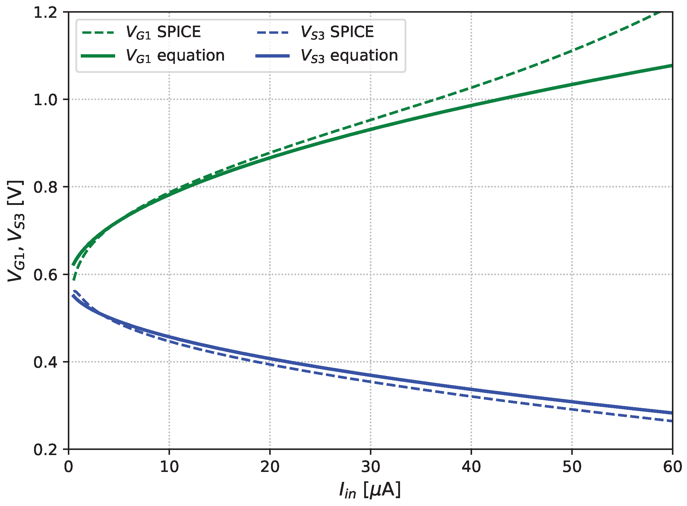
5.2. Design Example: Wide-Swing Cascode Current Mirror

To illustrate the practical application of the heuristic EKV model fitting method, we consider the wide-swing cascode current mirror depicted in Figure 8a [39]. In this implementation, all transistor bulks are grounded, and all transistors operate in strong inversion. Nominally, M1 and M2 are identical ( β 1 = β 2 ), as are M3 and M4 ( β 3 = β 4 ). The input and output currents are denoted as I i n and I o u t respecitvely. The voltage V N is set to ensure M4 saturation ( V N > V P 4 + V P 2 , being V P 4 and V P 2 , the pinch-off voltages of M4 and M2, respectively). The values allowed for the cascode control voltage, V C , are discussed in the following analysis.
Utilizing the approximate EKV strong inversion expression (Equation (4)), and the relationship β = I S / ( 2 U T 2 ) , we derive the following:
V G 1 = V T H 1 + 2 n 1 I i n β 1 = V T H 1 + 2 n 1 U T I i n I S 1
and
V P 1 = V G 1 V T H 1 n 1 = 2 U T I i n I S 1 .
Here, V T H 1 , n 1 , I S 1 , and V P 1 represent the threshold voltage, subthreshold slope factor, specific current, and pinch-off voltage of M1, respectively.
The first constraint, V D S 1 = V D 1 V P 1 , ensures M1 saturation. Given that V D 1 = V S 3 due to the M1–M3 stacking, M3 must also be considered.
To maintain current mirroring precision, M3 should also operate in saturation, leading to the second constraint: V D S 3 V P 3 = V C V T H 3 n 3 , where V D S 3 = V G 1 V S 3 .
These constraints yield the following inequalities:
V S 3 V P 1 , V G 1 V S 3 V P 3 .
Applying Equation (4) to M3, we find V S 3 :
V S 3 = 1 n 3 V P 3 2 n 3 U T I i n I S 3 = 1 n 3 V P 3 n 3 n 1 I S 1 I S 3 V P 1 ,
which, when substituted into Equation (15), gives the following:
V P 3 n 3 + n 3 n 1 I S 1 I S 3 V P 1 , V P 3 1 1 + n 3 n 1 n 3 + n 3 n 1 I S 1 I S 3 V P 1 + n 3 1 + n 3 V T H 1 .
Since V P 3 = V C V T H 3 n 3 , we can make V C explicit in the inequalities above:
V C n 3 n 3 + n 3 n 1 I S 1 I S 3 V P 1 + V T H 3 , V C n 3 1 + n 3 n 1 n 3 + n 3 n 1 I S 1 I S 3 V P 1 + n 3 2 1 + n 3 V T H 1 + V T H 3 .
Figure 8b illustrates the valid operating region for V C , given by the inequalities of Equation (18) and considering V P 1 I i n by virtue of Equation (14). The voltage intercept values of the plot, V C 1 and V C 2 , are determined from Equation (18) as I i n 0 ( V P 1 0 ):
V C 1 = V T H 3 , V C 2 = n 3 2 1 + n 3 V T H 1 + V T H 3 .
The green region in Figure 8b represents the valid operating area, defined by Equation (18). The shaded left area indicates the transition to moderate inversion at low current levels. The plot shows that a specific V C , indicated with V C , defines an I i n operating range ( I i n 1 I i n I i n 2 ), provided V C < V C , max . At V C = V C , max , the I i n interval reduces to a single point. For V C > V C , max , M3 enters the linear region.
Rather than utilizing these analytical expressions for circuit design, this work focuses on demonstrating the accuracy of the EKV model, with parameters extracted using the iterative subranging method, against BSIM4 simulations, using ngspice. Specifically, we compare the DC values of V G 1 and V S 3 as a function of I i n .
Transistor details and extracted parameters are summarized in Table 2. Parameter extraction was performed using fit_range_parameter = 1.65 for all devices, a value manually adjusted to ensure a current validity range of 2 µA to 60 µA. Based on the extracted parameters, V C 1 and V C 2 were estimated to be 609 mV and 939 mV, respectively. The bias voltages V C and V N were set to 1.3 V and 1.0 V, respectively.
Figure 9 illustrates the comparison between electrical simulation and the strong-inversion EKV approximation (Equations (13) and (16)) using the extracted parameters. While the simplified model provides acceptable accuracy within the gate voltage range reported in Table 2, it shows a visible deviation in the V G 1 trace for I i n > 30  µA. This deviation highlights the limitations of the simplified EKV model, which does not account for channel length modulation effects, as outlined in Section 2.2.

6. Conclusions

This work presents a novel approach to fitting the EKV model to MOSFET data using an iterative subranging technique. The proposed methodology is implemented in Python, with the core functionality encapsulated in the Fitter class. This provides a robust framework for extracting key MOSFET parameters, including the threshold voltage ( V T H ), the specific current ( I S ), and the subthreshold slope factor (n).
The iterative subranging technique is a key innovation of this work. By progressively narrowing the voltage range used for fitting, controlled by the fit_range_parameter, the method ensures accurate parameter extraction in the region of interest (e.g., weak inversion) while still considering the full range of data. This approach is particularly effective for low-power IC design, where accurate modeling of weak and moderate inversion regions is critical.
The implementation includes several practical features to enhance usability and robustness:
  • Flexibility: Users can control various aspects of the fitting process, such as the number of iterations (max_iter) and error margins (error_margin), allowing for tailored parameter extraction.
  • Fit Quality Assessment: The fit_quality function evaluates the quality of the fitted curve by comparing it to the measured data within a specified error margin (quality_margin). This provides a quantitative measure of the fitting accuracy and is particularly useful in design practice to increase confidence in preliminary analytical estimations prior to extensive electrical simulations.
  • Open-Source and Reproducibility: By leveraging open-source tools like scipy, numpy, and matplotlib, the implementation promotes reproducibility and accessibility, aligning with the principles of open science.
The proposed methodology was validated using measured data from a low-power MOSFET in the SkyWater130 technology, demonstrating its effectiveness across different regions of operation (weak, moderate, and strong inversion). The results highlight the method’s robustness against measurement noise and its ability to provide accurate parameter extraction even in the presence of uncertainties. Furthermore, a minimal design example has been discussed to demonstrate the practical benefits of the extraction methodology. The extracted parameters are specific to the SkyWater130 technology and may vary for other fabrication processes. However, the proposed methodology is adaptable to different technologies by adjusting the model and fitting parameters.
Future work could explore automated methods for selecting the fit_range_parameter and extending the approach to other device models and technologies. In the current implementation, the extraction methodology focused on only three model parameters: V T H , I S , and n, which are of paramount importance for DC and low-frequency operation of analog circuits, especially when designed with mature technologies. However, the proposed framework can be expanded to incorporate nanoscaled technologies and high-speed designs by including additional model parameters. Future work could incorporate more complex models to address short-channel effects and improve accuracy in advanced technologies.
The proposed methodology has significant potential for applications in low-power IC design, particularly for circuits operating in weak and moderate inversion regions. This includes subthreshold amplifiers and ultra-low-power sensor interfaces [40,41,42,43,44]. The Python implementation of the iterative subranging method is available as open-source software to facilitate its adoption and further development.

Funding

This work was supported by the National Recovery and Resilience Plan (NRRP), Mission 4 Component 2 Investment 1.2 of Italian MUR funded by European Union–NextGenerationEU through the Project: “Health Monitoring Wearable Platform” (HeMoWear), under Award 0004610/2022.

Data Availability Statement

The Python implementation of the heuristic iterative subranging technique for EKV model fitting, along with example data and usage instructions, is available in the GitHub repository at https://github.com/michele-dei/EKV-fit (accessed on 12 March 2025). This repository includes all necessary code, documentation, and sample datasets to reproduce the results presented in this work.

Acknowledgments

During the preparation of this manuscript/study, the author used DeepSeek v3 [45] for the purposes of checking the grammar, the spelling, and the fluency of the draft text. The draft text was prepared before the use of the AI tool. The author has reviewed and edited the output and takes full responsibility for the content of this publication. All experiments conducted using other software (Python scripts, Python version 3.10.12) were produced and scripted by the author. The interpretation of the data was performed by the author.

Conflicts of Interest

The author declares no conflicts of interest. The funders had no role in the design of the study; in the collection, analyses, or interpretation of data; in the writing of the manuscript; or in the decision to publish the results.

Appendix A

Appendix A.1. Simplified Fitter Class Code

The Fitter class is the core part of the flowchart shown in Figure 2. It is designed to streamline the process of characterizing MOSFETs using the EKV model. Below is a simplified version of the Fitter class code, highlighting its main algorithmic features. The full code can be found in the referenced GitHub repository [46]. This class encapsulates the data reading and EKV model fitting functionalities. The __init__ method initializes the class with the input parameters, reads the data using _read_data, and performs the fitting using _fit_data. The _fit_data method implements the core iterative fitting algorithm, refining the threshold voltage and assessing the fit quality.
Electronics 14 01162 i001a
Electronics 14 01162 i001b

Appendix A.2. Step-by-Step Basic Usage

1.
Initializing the Fitter class: to begin, create an instance of the Fitter class. This involves specifying the path to your data file and optionally, setting any specific fitting parameters.
Electronics 14 01162 i002
2.
Accessing the results: once the Fitter object is set up, it automatically begins the fitting process. The results are stored as attributes of the Fitter instance, including the fitted parameters and quality metrics.
Electronics 14 01162 i003
3.
Customizing the fitting process: by adjusting parameters like fit_range_parameter, error_margin, and quality_margin, you can tailor the fitting process to meet the specific needs of your analysis.
4.
Leveraging additional features: beyond the basic fitting process, the Fitter class includes additional capabilities such as current logarithmic scaling (see Section 3.2) and extended plotting options for detailed analysis.

References

  1. Gielen, G.; De Graaf, H.C.; Sansen, W.M.C. A new efficient MOS transistor model (BSIM) for circuit simulation. In Proceedings of the 1990 IEEE International Symposium on Circuits and Systems, New Orleans, LA, USA, 1–3 May 1990; pp. 182–185. [Google Scholar] [CrossRef]
  2. Sheu, B.J.; Scharfetter, D.L.; Ko, P.K.; Jeng, M.C. BSIM: Berkeley short-channel IGFET model for MOS transistors. IEEE J. Solid-State Circuits 1987, 22, 558–566. [Google Scholar] [CrossRef]
  3. Cheng, Y.; Hu, C. MOSFET Modeling & BSIM3 User’s Guide; Springer: New York, NY, USA, 1999. [Google Scholar]
  4. Schichman, H.; Hodges, D.A. Modeling and simulation of insulated-gate field-effect transistor switching circuits. IEEE J. Solid-State Circuits 1968, 3, 285–289. [Google Scholar] [CrossRef]
  5. Enz, C.C.; Krummenacher, F.; Vittoz, E.A. An analytical MOS transistor model valid in all regions of operation and dedicated to low-voltage and low-current applications. Analog Integr. Circuits Signal Process. 1995, 8, 83–114. [Google Scholar] [CrossRef]
  6. Enz, C.C.; Vittoz, E.A. CMOS low-power analog circuit design. In Emerging Technologies: Designing Low Power Digital Systems; IEEE: Piscataway, NJ, USA, 1996; pp. 79–133. [Google Scholar] [CrossRef]
  7. Enz, C.C.; Vittoz, E.A. Charge-Based MOS Transistor Modeling: The EKV Model for Low-Power and RF IC Design; Wiley: Hoboken, NJ, USA, 2006. [Google Scholar]
  8. Enz, C.; Chicco, F.; Pezzotta, A. Nanoscale MOSFET modeling: Part 1: The simplified EKV model for the design of low-power analog circuits. IEEE Solid-State Circuits Mag. 2017, 9, 26–35. [Google Scholar] [CrossRef]
  9. Enz, C.; Chicco, F.; Pezzotta, A. Nanoscale MOSFET modeling: Part 2: Using the inversion coefficient as the primary design parameter. IEEE Solid-State Circuits Mag. 2017, 9, 73–81. [Google Scholar] [CrossRef]
  10. Serra-Graells, F. VLSI CMOS low-voltage log companding filters. In Proceedings of the 2000 IEEE International Symposium on Circuits and Systems (ISCAS), Geneva, Switzerland, 28–31 May 2000; Volume 1, pp. 172–175. [Google Scholar] [CrossRef]
  11. Sansen, W. Biasing for zero distortion: Using the EKV/BSIM6 expressions. IEEE Solid-State Circuits Mag. 2018, 10, 48–53. [Google Scholar] [CrossRef]
  12. Xie, Q.; Xu, J.; Taur, Y. Review and Critique of Analytic Models of MOSFET Short-Channel Effects in Subthreshold. IEEE Trans. Electron Devices 2012, 59, 1569–1579. [Google Scholar] [CrossRef]
  13. Chaudhry, A.; Roy, J.N. MOSFET models, quantum mechanical effects and modeling approaches: A review. JSTS J. Semicond. Technol. Sci. 2010, 10, 20–27. [Google Scholar] [CrossRef]
  14. Cerederia, A.; Estrada, M.; Alvardo, J.; Garduno, I.; Contreras, E.; Tinoco, J. Review On Double Gate Mosfets and Finfet Modelling. Electron. Energ. 2013, 26, 197–213. [Google Scholar]
  15. Chauhan, Y.S.; Venugopalan, S.; Chalkiadaki, M.-A.; Karim, M.A.U.; Agarwal, H.; Khandelwal, S. BSIM6: Analog and RF Compact Model for Bulk MOSFET. IEEE Trans. Electron. Dev. 2014, 61, 234–244. [Google Scholar] [CrossRef]
  16. BSIM Group at UC Berkeley. The BSIM Family. Available online: https://www.bsim.berkeley.edu/models/ (accessed on 4 March 2025).
  17. Mattausch, H.J.; Miura-Mattausch, M.; Sadachika, N.; Miyake, M.; Navarro, D. The HiSIM compact model family for integrated devices containing a surface-potential MOSFET core. In Proceedings of the 2008 15th International Conference on Mixed Design of Integrated Circuits and Systems, Poznan, Poland, 19–21 June 2008; pp. 39–50. [Google Scholar]
  18. Bhattacharyya, A.B. Semiconductor Physics Review for MOSFET Modeling. In Compact MOSFET Models for VLSI Design; IEEE: New York, NY, USA, 2009; pp. 1–53. [Google Scholar] [CrossRef]
  19. Gildenblat, G.; Wu, W.; Li, X.; Zhu, Z.; Smit, G.D.J.; Scholten, A.J.; Klaassen, D.B.M. Surface-potential-based MOSFET models with introduction to PSP (invited). In Proceedings of the 2009 IEEE 10th Annual Wireless and Microwave Technology Conference, Clearwater, FL, USA, 20–21 April 2009; pp. 1–2. [Google Scholar] [CrossRef]
  20. Araujo-Cunha, A.I.; Schneider, M.C.; Galup-Montoro, C. An MOS transistor model for analog circuit design. IEEE J. Solid-State Circuits 1998, 33, 1510–1519. [Google Scholar] [CrossRef]
  21. Sansen, W.M. Analog Design Essentials; Springer Science & Business Media: Berlin/Heidelberg, Germany, 2007; Volume 859. [Google Scholar]
  22. Jespers, P. The gm/ID Methodology, a Sizing Tool for Low-Voltage Analog CMOS Circuits: The Semi-Empirical and Compact Model Approaches; Springer Science & Business Media: Berlin/Heidelberg, Germany, 2009. [Google Scholar]
  23. Sansen, W. Minimum power in analog amplifying blocks: Presenting a design procedure. IEEE Solid-State Circuits Mag. 2015, 7, 83–89. [Google Scholar] [CrossRef]
  24. Neto, D.G.A.; Bouchoucha, M.K.; Maranhão, G.; Barragan, M.J.; Schneider, M.C.; Cathelin, A.; Galup-Montoro, C. Design-oriented single-piece 5-DC-parameter MOSFET model. IEEE Access. 2024, 12, 87420–87437. [Google Scholar] [CrossRef]
  25. Bucher, M.; Lallement, C.; Enz, C.; Theodoloz, F.; Krummenacher, F. The EPFL-EKV MOSFET Model Equations for Simulation, Model Version 2.6; Electronics Laboratories, Swiss Federal Institute of Technology (EPFL): Lausanne, Switzerland, 1997. [Google Scholar]
  26. Bucher, M.; Lallement, C.; Enz, C.C. An efficient parameter extraction methodology for the EKV MOST model. In Proceedings of the International Conference on Microelectronic Test Structures, Osaka, Japan, 25–28 March 1996; pp. 145–150. [Google Scholar] [CrossRef]
  27. Li, X.; Gildenblat, G. Robust parameter extraction for MOSFET models. IEEE Trans. Electron Devices 2009, 56, 952–958. [Google Scholar] [CrossRef]
  28. Bajer, K.; Paul, S.; Peters-Drolshagen, D. Parameter extraction for a simplified EKV-model in a 28nm FDSOI technology. In Proceedings of the 2020 27th International Conference on Mixed Design of Integrated Circuits and System (MIXDES), Wrocław, Poland, 25–27 June 2020; pp. 45–49. [Google Scholar] [CrossRef]
  29. Serra-Graells, F.; Rueda, A.; Huertas, J.L. Low-Voltage CMOS Log Companding Analog Design; Springer: New York, NY, USA, 2006; Volume 733. [Google Scholar]
  30. Ajayi, T.; Blaauw, D.; Chan, T.B.; Cheng, C.K.; Chhabria, V.; Choo, D.K.; Coltella, M.; Dreslinski, R.; Fogaça, M.; Hashemi, S.; et al. OpenROAD: Toward a self-driving, open-source digital layout implementation tool. IEEE Trans. Comput.-Aided Des. Integr. Circuits Syst. 2020, 39, 2925–2936. [Google Scholar]
  31. Gagliardi, F.; Dei, M. Open and Collaborative Dataset for the Classification of Operational Transconductance Amplifiers for Switched-Capacitor Applications. Data 2024, 9, 114. [Google Scholar] [CrossRef]
  32. Reda, S.; Stok, L.; Gaillardon, P.E. Guest Editors’ Introduction: The Resurgence of Open-Source EDA Technology. IEEE Des. Test 2021, 38, 5–7. [Google Scholar] [CrossRef]
  33. Goyal, C.; Khandeparkar, H.; Charan, S.; Baquero, J.S.; Li, A.; Euphrosine, J.; Saligane, M. Disrupting conventional chip design through the open source EDA ecosystem. In Proceedings of the 2024 8th IEEE Electron Devices Technology & Manufacturing Conference (EDTM), Singapore, 10–13 March 2024; pp. 1–3. [Google Scholar] [CrossRef]
  34. Kahng, A.B. Open-source EDA: If we build it, who will come? In Proceedings of the 2020 IFIP/IEEE 28th International Conference on Very Large Scale Integration (VLSI-SOC), Salt Lake City, UT, USA, 6–9 October 2020; pp. 1–6. [Google Scholar] [CrossRef]
  35. Galán-Benítez, I.; Carmona-Galán, R.; de la Rosa, J.M. On the use of open-source EDA tools for teaching and learning microelectronics. In Proceedings of the 2024 XVI Congreso de Tecnología, Aprendizaje y Enseñanza de la Electrónica (TAEE), Valencia, Spain, 19–21 June 2024; pp. 1–6. [Google Scholar] [CrossRef]
  36. Koohang, A.; Harman, K. Open source: A metaphor for e-learning. Inform. Sci. 2005, 8, 75–86. [Google Scholar] [CrossRef]
  37. scipy.optimize.curve_fit, SciPy v1.13.0 Manual; SciPy: Austin, TX, USA, 2023; Available online: https://docs.scipy.org/doc/scipy/reference/generated/scipy.optimize.curve_fit.html (accessed on 7 January 2025).
  38. Virtanen, P.; Gommers, R.; Oliphant, T.E.; Haberland, M.; Reddy, T.; Cournapeau, D.; Burovski, E.; Peterson, P.; Weckesser, W.; Bright, J.; et al. SciPy 1.0: Fundamental algorithms for scientific computing in Python. Nat. Methods 2020, 17, 261–272. [Google Scholar] [CrossRef]
  39. Carusone, T.C.; Johns, D.A.; Martin, K.W. Analog Integrated Circuit Design; John Wiley & Sons: Hoboken, NJ, USA, 2011; Chapter 6. [Google Scholar]
  40. Ria, A.; Cicalini, M.; Bruschi, P.; Piotto, M.; Dei, M. Wide-Range Low-Power Low-Voltage Integrated Capacitance-to-Digital Converter for On-Body Sweat-Rate Sensing. IEEE Sens. J. 2025, 25, 10250–10260. [Google Scholar] [CrossRef]
  41. Catania, A.; Gagliardi, F.; Piotto, M.; Bruschi, P.; Dei, M. Ultralow-Power Inverter-Based Delta-Sigma Modulator for Wearable Applications. IEEE Access 2024, 12, 80009–80019. [Google Scholar] [CrossRef]
  42. Gagliardi, F.; Ria, A.; Piotto, M.; Bruschi, P. A 114 ppm/oC-TC 0.78%-(σ/μ) Current Reference with Minimum-Current-Search Calibration. IEEE Trans. Circuits Syst. II Express Briefs 2024, 71, 1561–1565. [Google Scholar] [CrossRef]
  43. Aymerich, J.; Ferrer-Vilanova, A.; Cisneros-Fernández, J.; Escudé-Pujol, R.; Guirado, G.; Terés, L.; Dei, M.; Muñoz-Berbel, X.; Serra-Graells, F. Ultrasensitive bacterial sensing using a disposable all-in-one amperometric platform with self-noise cancellation. Biosens. Bioelectron. 2023, 234, 115342. [Google Scholar] [CrossRef] [PubMed]
  44. Aymerich, J.; Márquez, A.; Muñoz-Berbel, X.; Del Campo, F.J.; Guirado, G.; Terés, L. A 15-µW 105-dB 1.8-Vpp Potentiostatic Delta-Sigma Modulator for Wearable Electrochemical Transducers in 65-nm CMOS Technology. IEEE Access 2020, 8, 62127–62136. [Google Scholar] [CrossRef]
  45. DeepSeek. DeepSeek-V3: Artificial Intelligence Model. 2024. Available online: https://www.deepseek.com (accessed on 24 January 2025).
  46. Dei, M. EKV-Fit: A Python Library for EKV MOSFET Model Fitting; GitHub Repository. 2024. Available online: https://github.com/michele-dei/EKV-fit (accessed on 12 March 2025).
Figure 1. I D - V G data extraction test bench.
Electronics 14 01162 g001
Figure 2. Operative framework using the proposed parameter extraction method: Initially, the designer sets up the SPICE test bench to extract I D - V G data. These data are then processed by the parameter extraction script. The functional flowchart of the parameter extraction script is described in detail to show implementation specifics. ϵ V T H is defined in Equation (11). Key sections of the Python code are provided in Appendix A.
Electronics 14 01162 g002
Figure 3. Fitting of the primitive nfet_01v8 devices ( W / L = 0.4 µm/0.33 µm, W / L = 4 µm/3.3 µm, W / L = 40 µm/33 µm) from SkyWater130 technology for different fit_range_parameter values: the thin traces indicate the experimental data (SPICE), the dotted traces indicate the fitted characteristics with the extracted EKV parameters, the thick traces indicate the interval where the relative error (from Equation (12)) is below 5%. (a) fit_range_parameter = 1.1, adjusted for accurate modeling of the moderate inversion region; (b) fit_range_parameter = 1.001, adjusted for accurate modeling of weak inversion region; (c) fit_range_parameter = 1.6, adjusted for accurate modeling of the strong inversion region.
Electronics 14 01162 g003
Figure 4. Fit quality assesment plot (a): accuracy comparison of fittings (log-scaled, Enz–Chicco–Pezzotta, and proposed iterative subranging). Device aspect ratio: 0.4 µm/0.33 µm, fit_range_parameter = 1.1. The shaded green area corresponds where the relative fitting error of the iterative subranging fitting, as defined from Equation (12), is systematically below 5%. (b) Fitting using the log-scaled method. (c) Fitting using the Enz–Chicco–Pezzotta method.
Electronics 14 01162 g004
Figure 5. Sensitivity of extracted EKV parameters to fit_range_parameter for a 0.4 µm/0.33 µm NMOS device. The plots illustrate the variation in (a) threshold voltage ( V T H ), (b) specific current ( I S ), and (c) subthreshold slope factor (n) as a function of fit_range_parameter for the proposed iterative subranging (ISR) method. For comparison, the constant parameter values obtained from the logarithmic scaling (logS) and Enz–Chicco–Pezzola (ECP) fitting methods are also shown. The upper ( V H ) and lower ( V L ) bounds of the V G validity interval are included in the V T H plot, demonstrating the impact of fit_range_parameter on the fitting range.
Electronics 14 01162 g005
Figure 6. Effects of noise on the fitting parameters: V T H , I S , and n. Black dot markers indicate mean values, while error bars indicate standard deviations. Each point was calculated from 1000 samples. In all cases, fit_range_parameter = 1.1 (0.4 µm/0.33 µm NMOS device).
Electronics 14 01162 g006
Figure 7. Impact of noise on parameter extraction ( σ I = 1 nA). (a) ISR method, showing robust fitting. (b) logS method, showing significant parameter deviations due to noise.
Electronics 14 01162 g007
Figure 8. Wide-swing cascode current mirror: (a) schematic; (b) valid operation region of V G 5 as a function of I i n .
Electronics 14 01162 g008
Figure 9. Electrical simulation (SPICE) vs. strong-inversion approximated expression of the EKV model (Equations (13) and (16)) using the proposed extraction method for transistor parameters ( V T H , I S , and n): V G 1 ( I i n ) and V S 3 ( I i n ) ; schematic in Figure 8a.
Electronics 14 01162 g009
Table 1. Effects of fit_range_parameter value on the IC region covered by the fitting ( W / L = 0.4 µm/0.33 µm case).
fit_range_parameterExtracted I S I D Validity IntervalIC Interval
[µA][µA]Equation (5)
1.0010.5740.001–0.515≈0.001–0.9
1.1001.0150.006–6.644≈0.006–6.5
1.6000.5340.356–25.842≈0.7–48
Table 2. Design details of the wide-swing cascode mirror of Figure 8. fit_range_parameter = 1.65.
Device M1, M2M3, M4
W, L[µm]2.0, 1.02.0, 0.5
Extracted V T H [mV]578609
Extracted I S [µA]0.8451.413
Extracted n 1.1461.095
Valid current range[µA]0.9–57.91.9–105.7
Valid gate voltage range[V]0.61–1.080.65–1.09
Disclaimer/Publisher’s Note: The statements, opinions and data contained in all publications are solely those of the individual author(s) and contributor(s) and not of MDPI and/or the editor(s). MDPI and/or the editor(s) disclaim responsibility for any injury to people or property resulting from any ideas, methods, instructions or products referred to in the content.

