


High Step-Up Interleaved DC–DC Converter with Voltage-Lift Capacitor and Voltage Multiplier Cell


Abstract
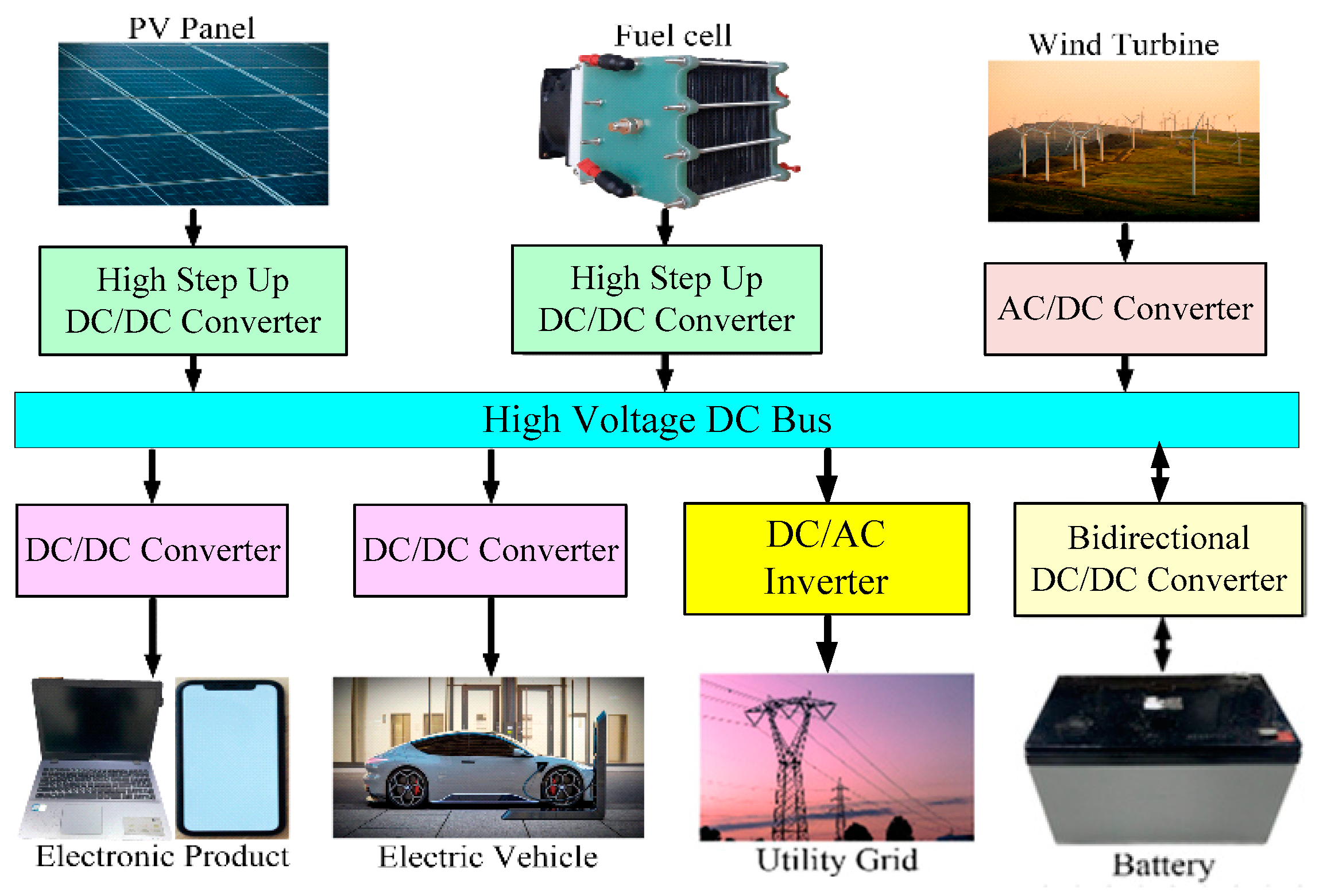
1. Introduction
- (1)
- The voltage gain is determined by two parameters: the duty ratio and the turns ratio of the coupled inductor. A high voltage gain of the presented converter can be realized with a reasonable duty ratio.
- (2)
- MOSFETs with low RDS(ON) can be adopted to reduce conduction losses because of low switch voltage stress. Additionally, the switches are turned on under zero-current switching (ZCS), which helps minimize switching losses.
- (3)
- Diodes with low forward voltage drops can be used to help cut down on conduction losses because of the lower voltage stress.
- (4)
- The leakage energy can be recycled to prevent voltage spikes during switch turn-off.
- (5)
- The parallel input architecture and interleaved operation help cut down on the current stress on each switch and decrease the input current ripple.
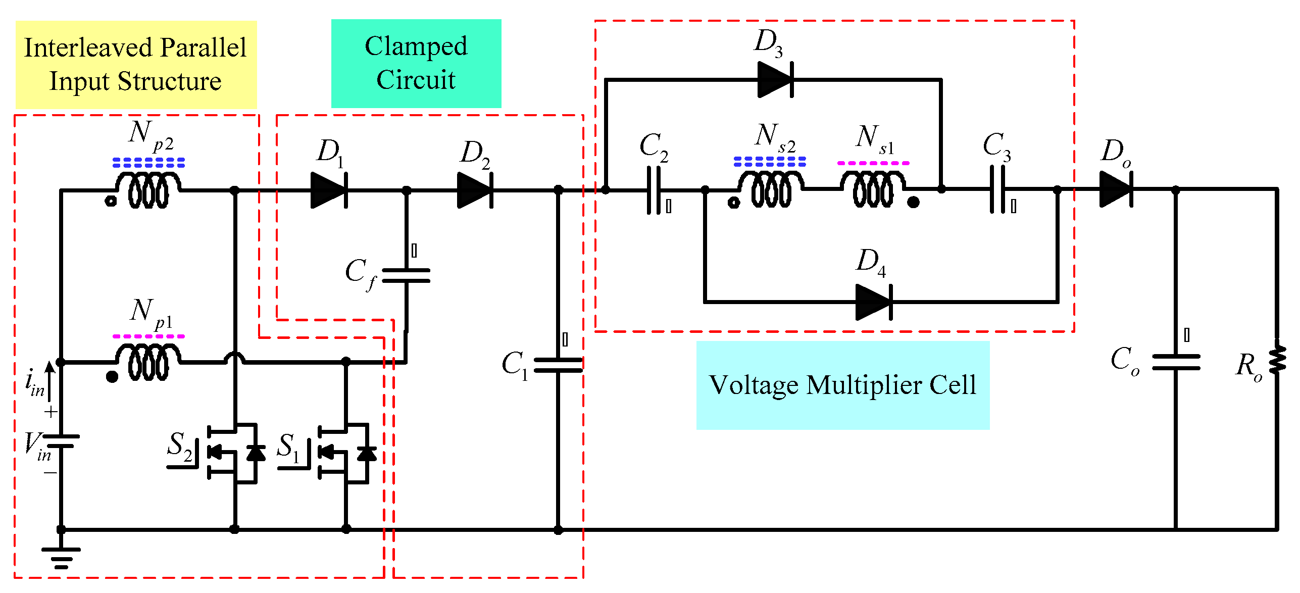
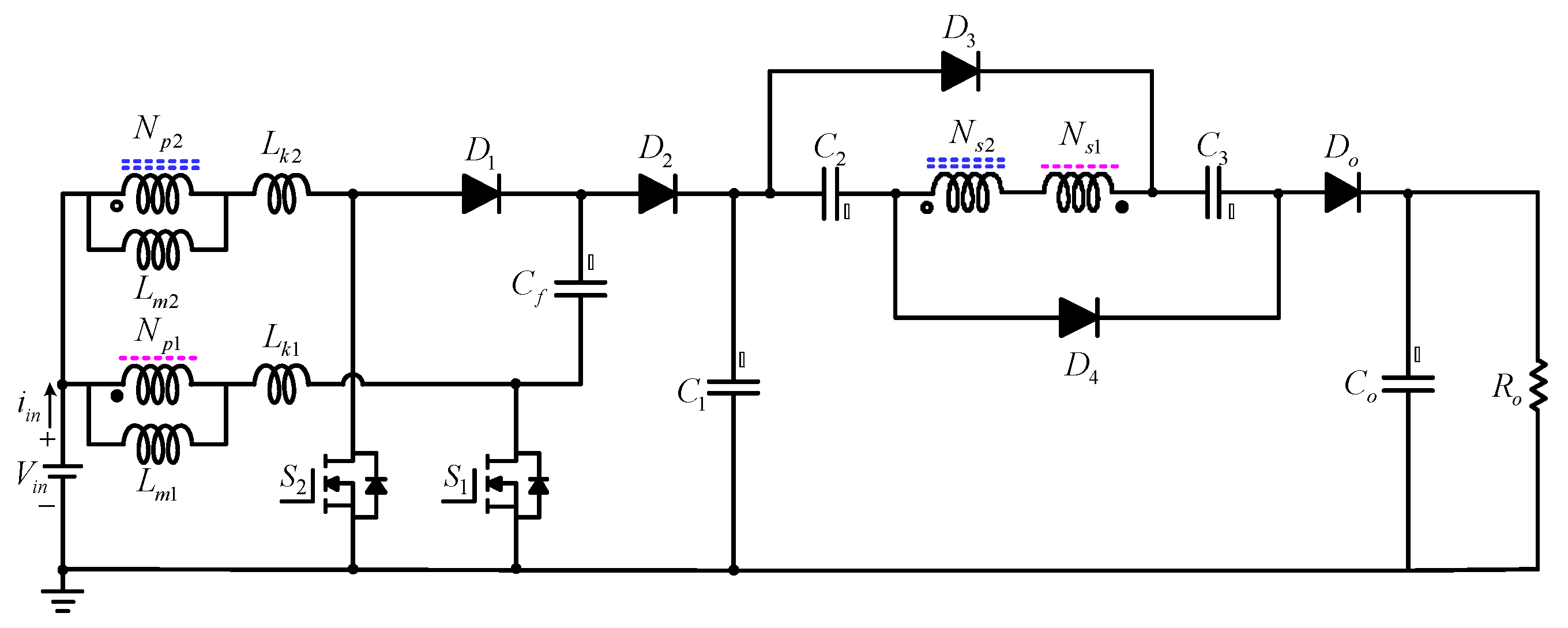
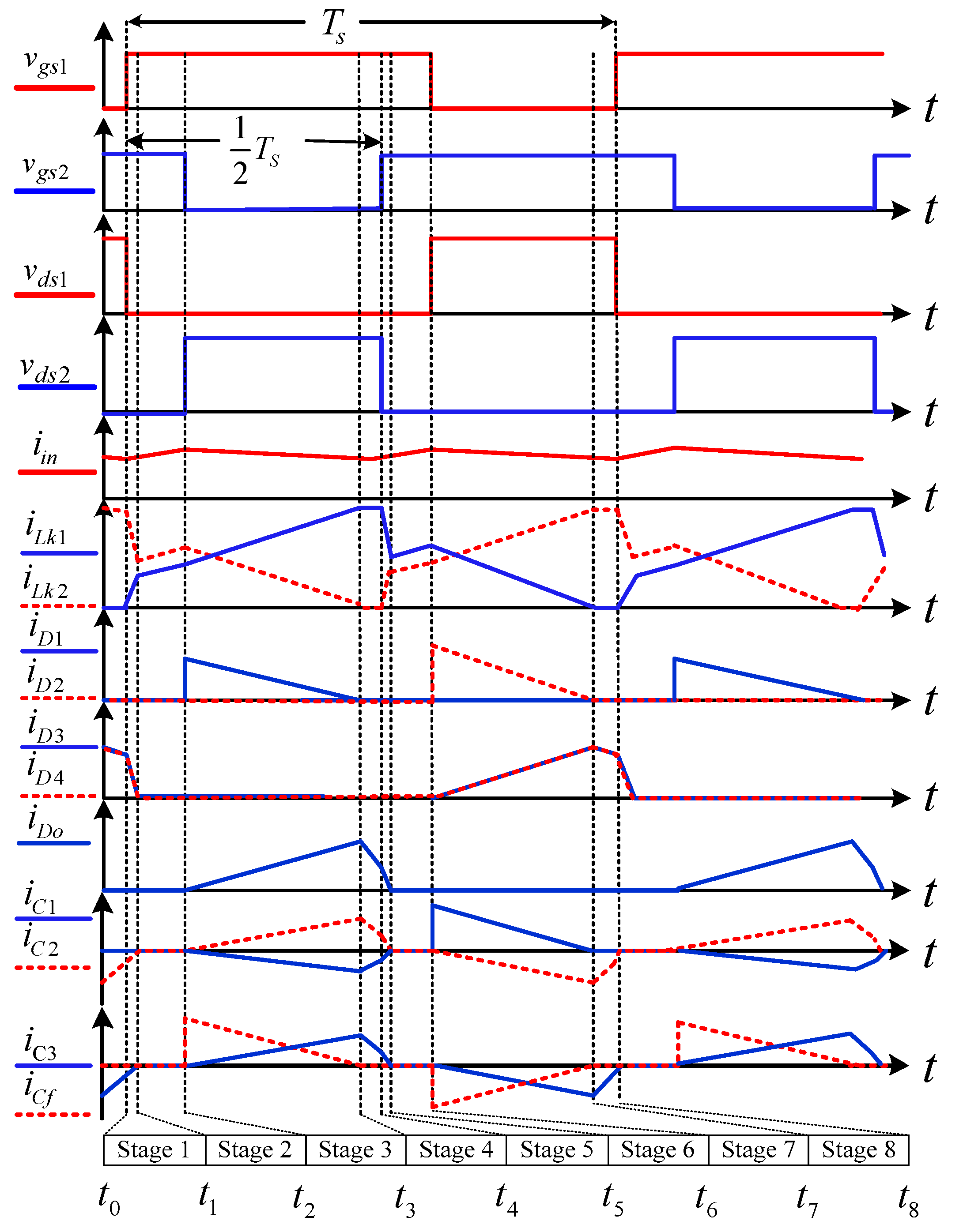
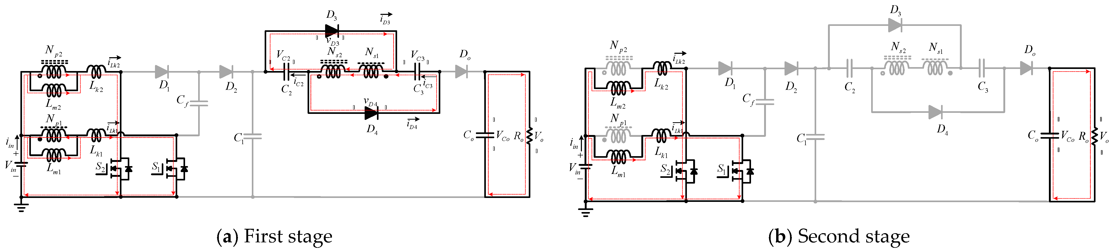
2. Converter Circuit and Operating Principles
3. Steady-State Analysis
- (1)
- All the semiconductors, including switches and diodes, are ideal.
- (2)
- All the capacitors are large enough to regard their voltages as constant.
- (3)
- The parameters of the two coupled inductors are assumed to be identical, including the magnetizing inductance, the leakage inductance, the turns ratios, and the coupling coefficient defined as .
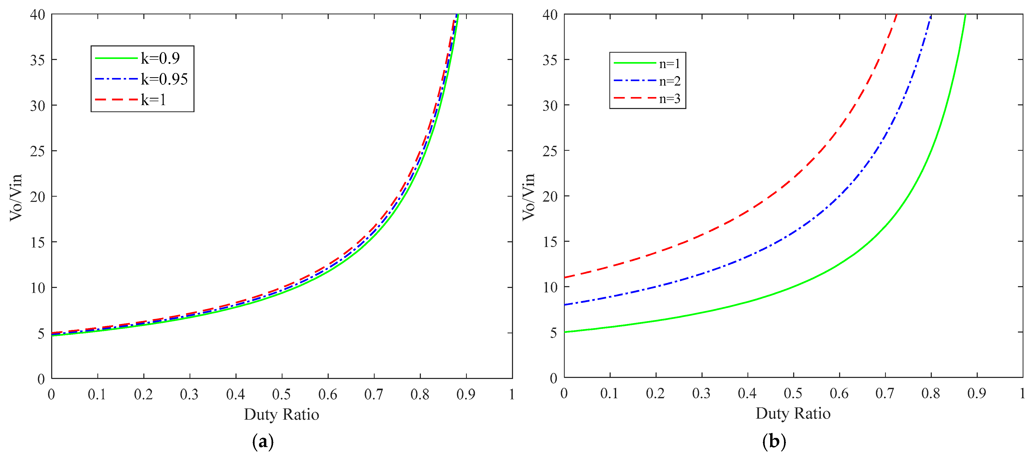
3.1. Voltage Gain Derivation
3.2. Voltage Stresses on Semiconductors
3.3. Key Performance Comparison
4. Design Considerations
4.1. Coupled Inductor Design
4.2. Capacitor Design
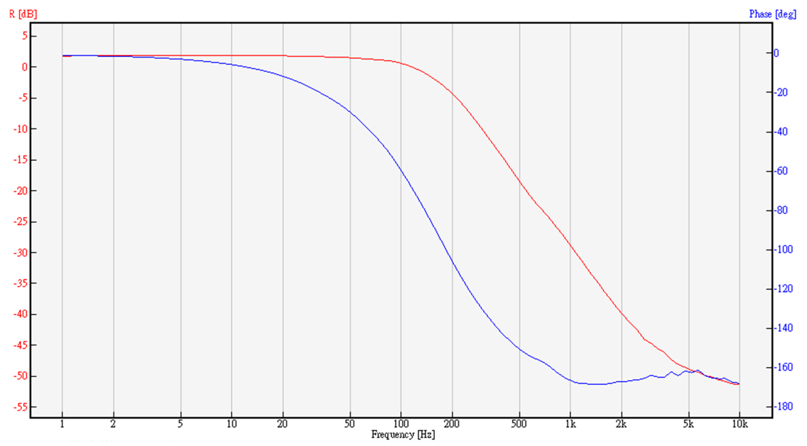
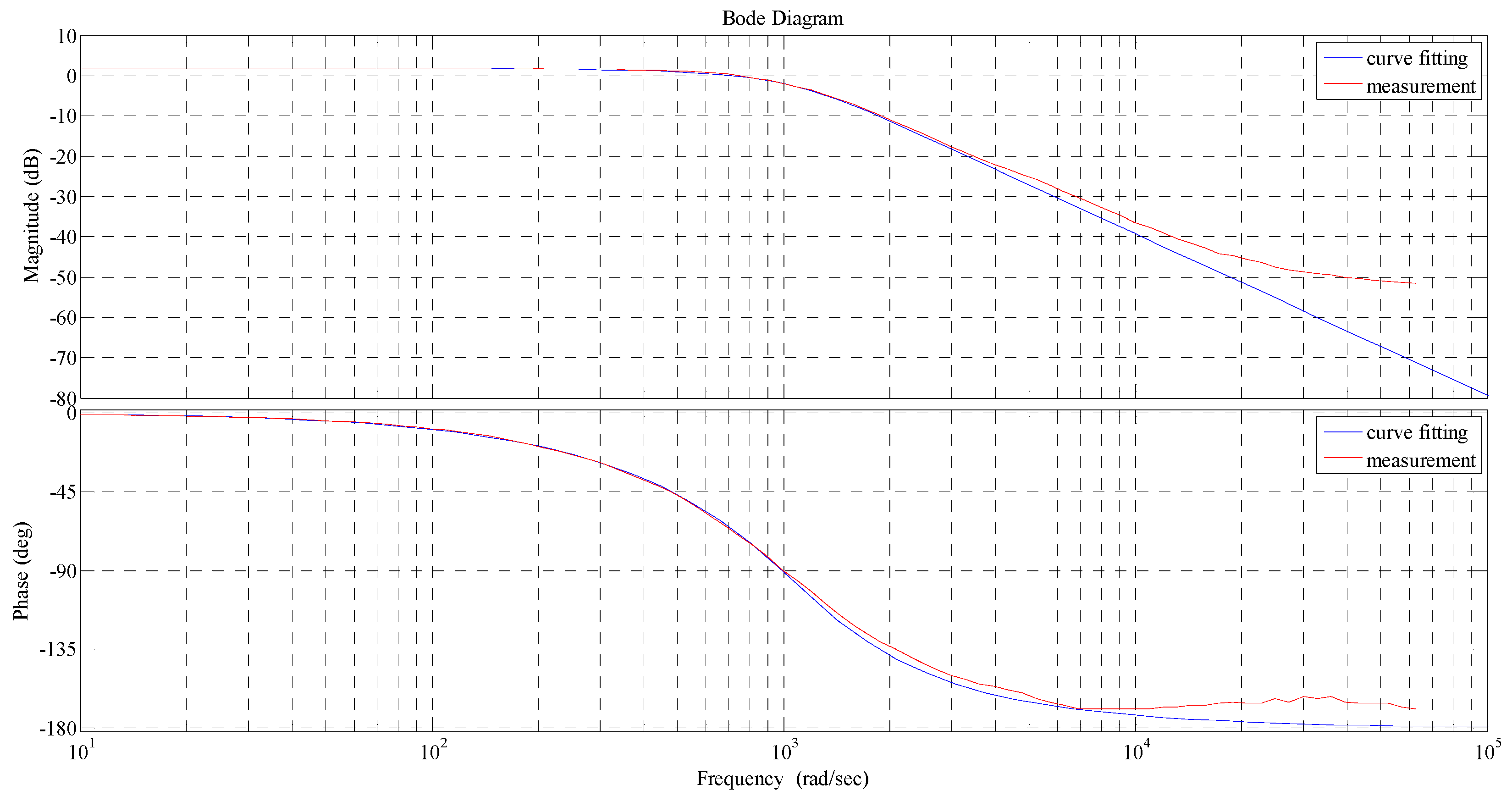
5. Feedback Control System Design
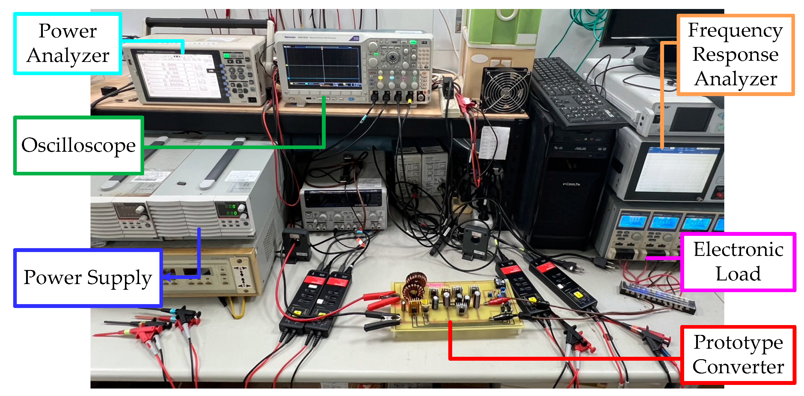
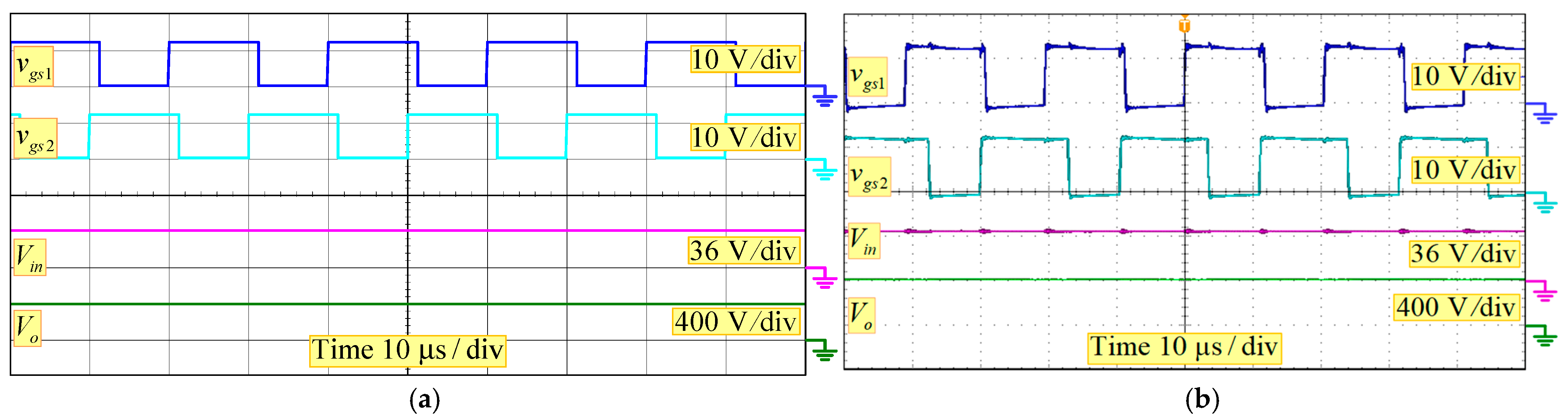
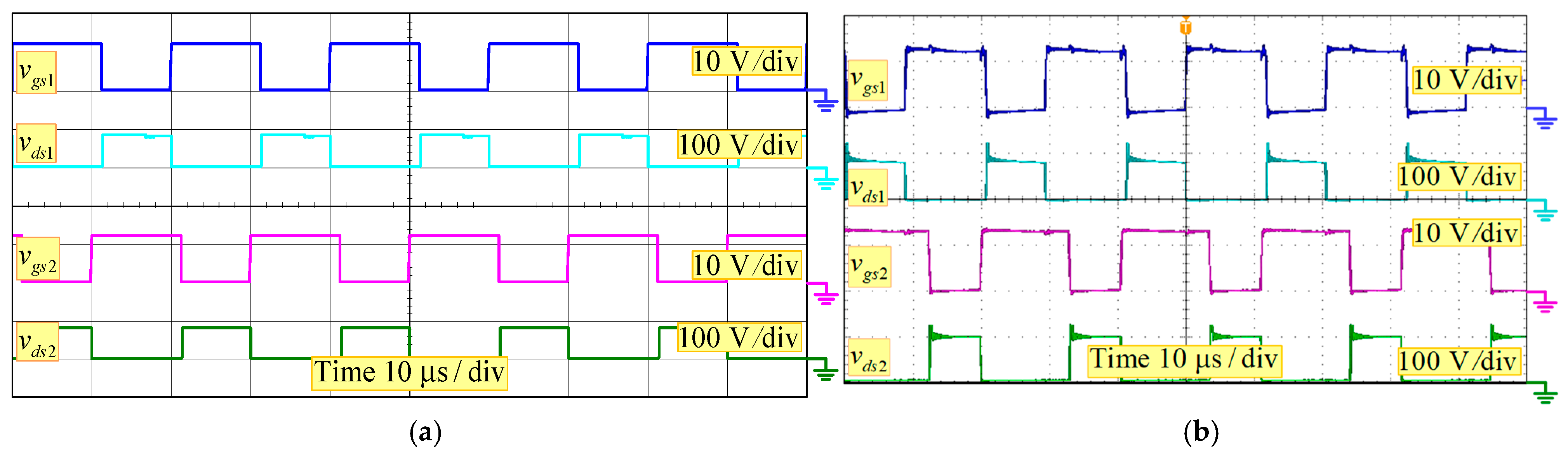
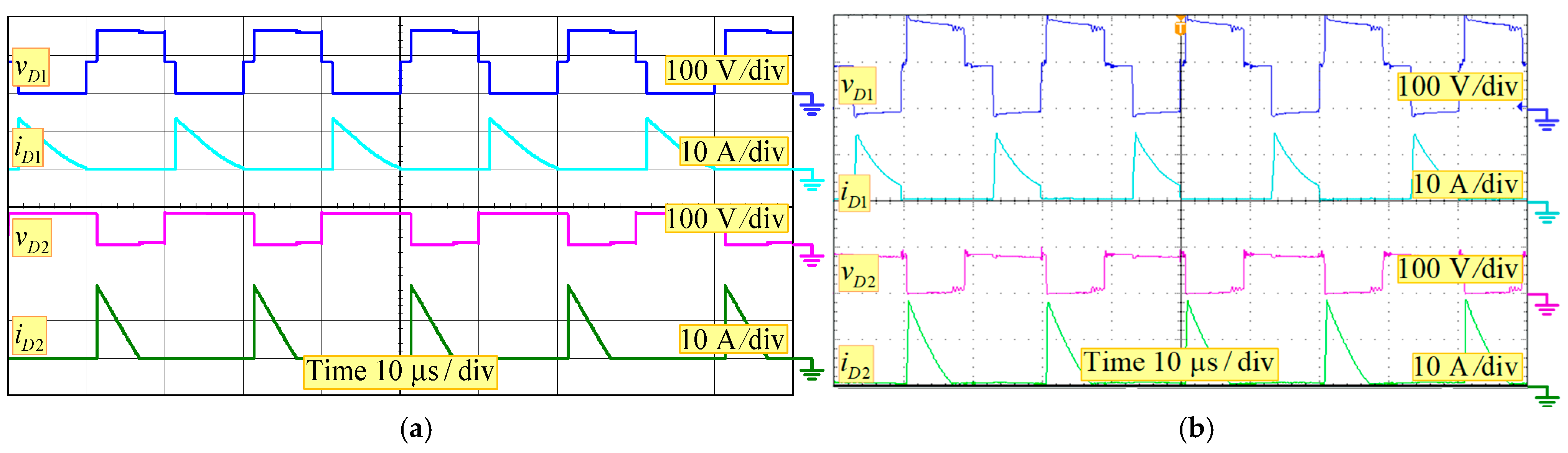
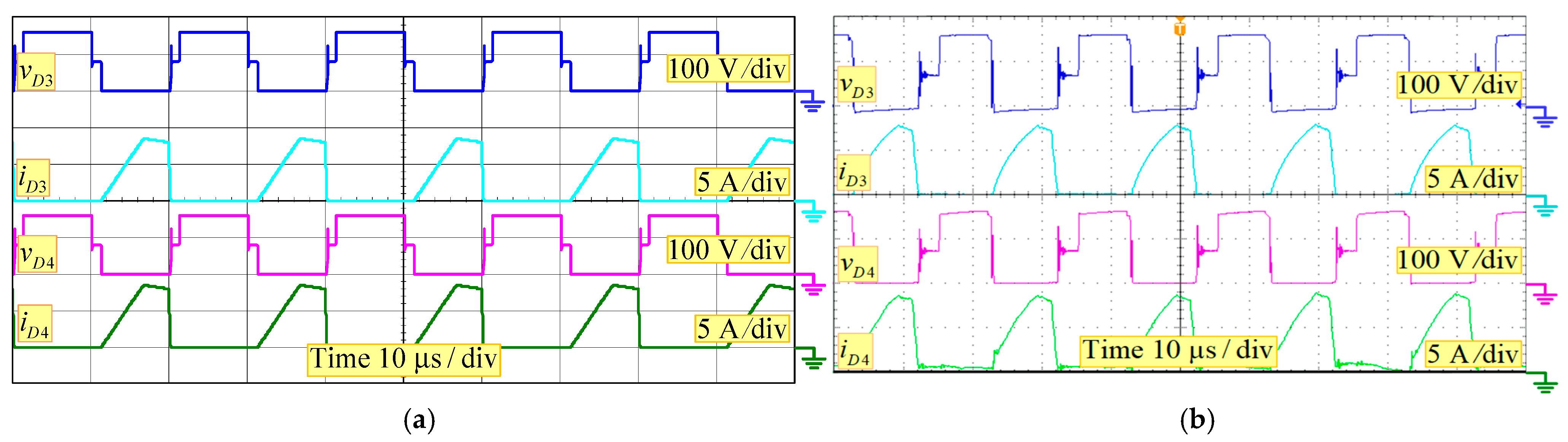
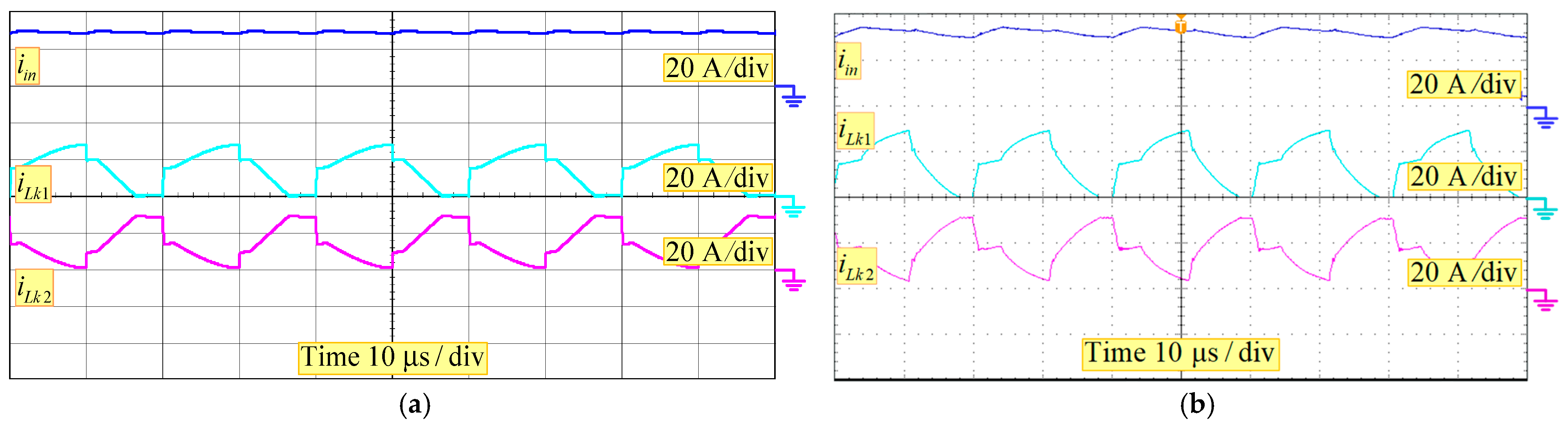
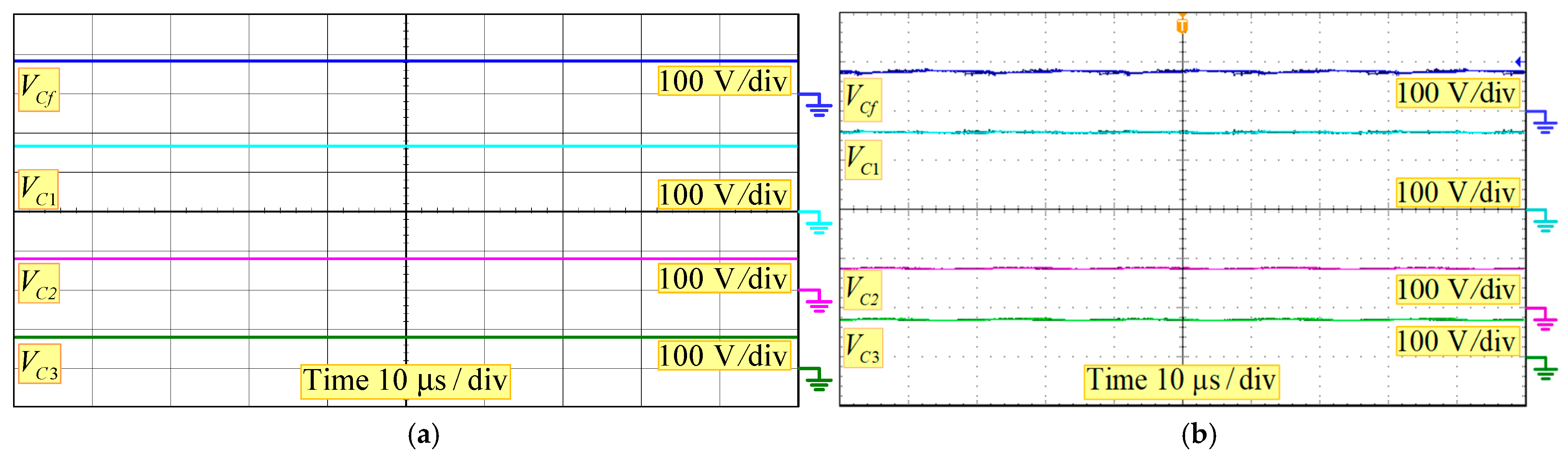
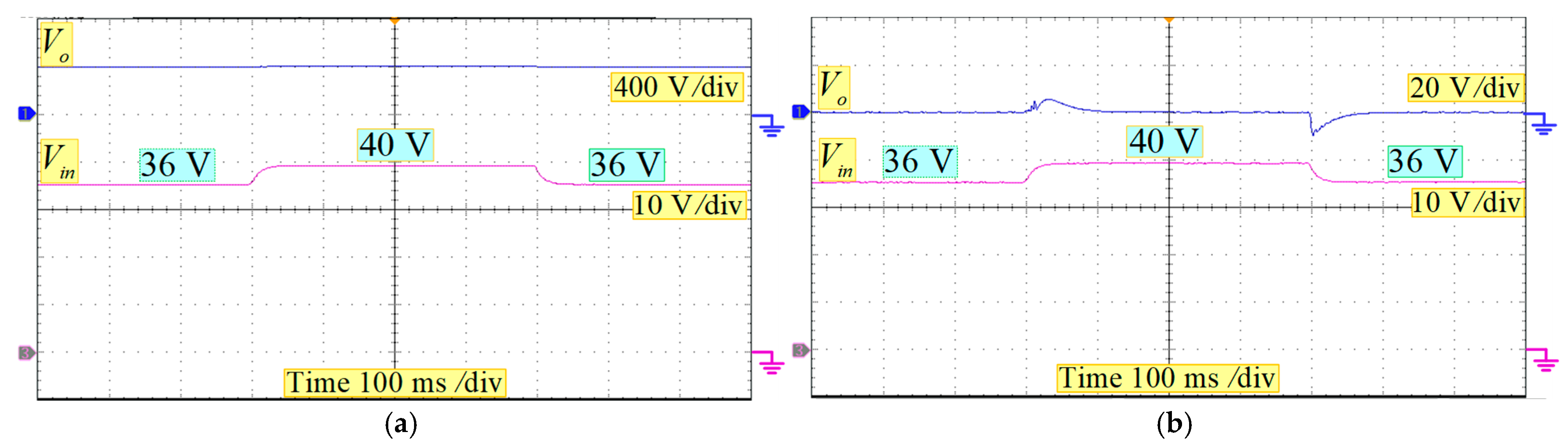
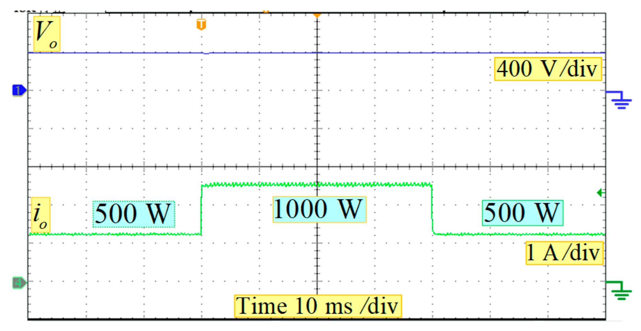
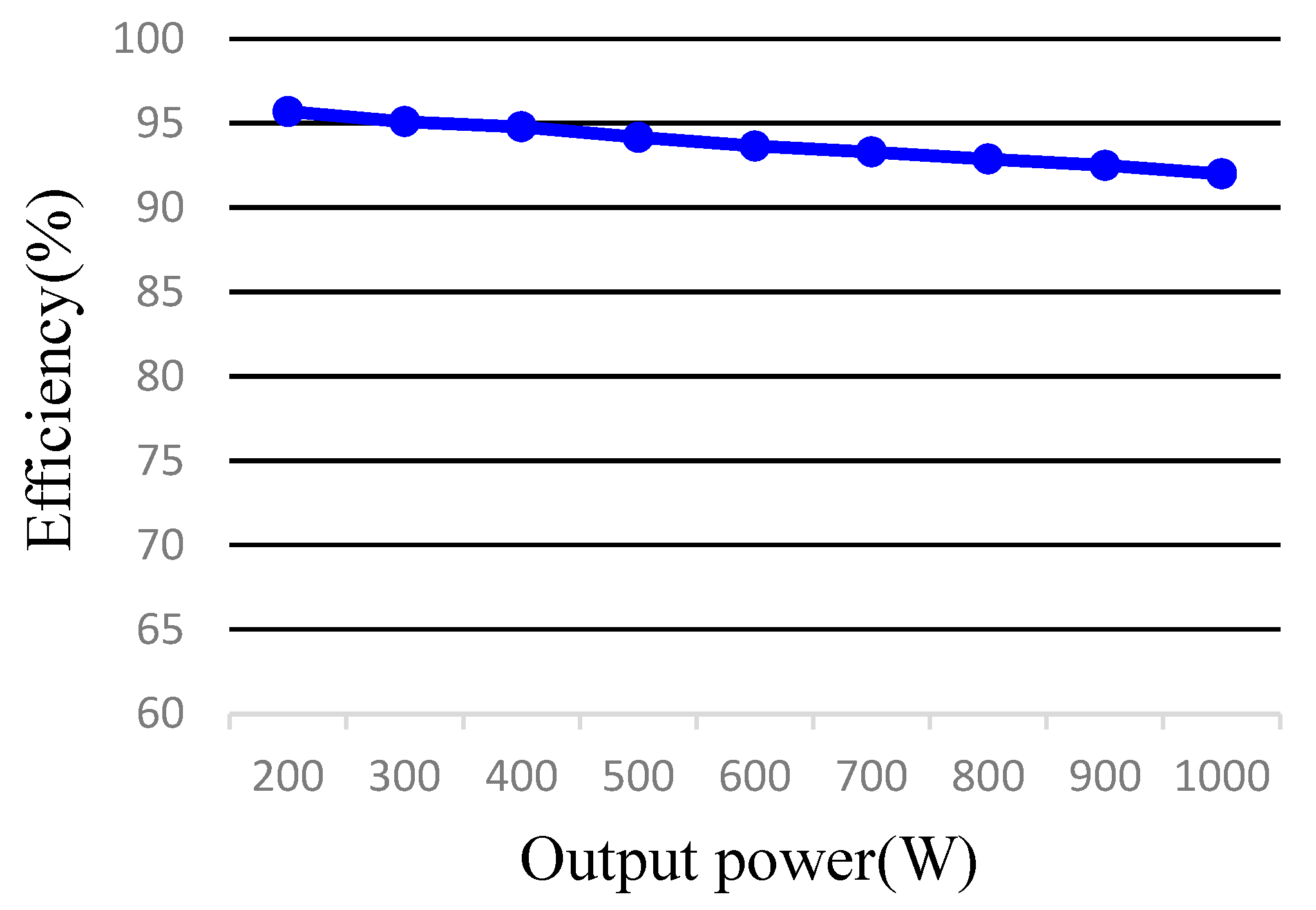
6. Experimental Verifications
7. Conclusions
Author Contributions
Funding
Data Availability Statement
Conflicts of Interest
References
- Zhang, X.; Gerada, D.; Xu, Z.; Zhang, F.; Gerada, C. A Review of carbon emissions from electrical machine materials. Electronics 2024, 13, 1714. [Google Scholar] [CrossRef]
- Zhang, L.; Sun, K.; Xing, Y.; Feng, L.; Ge, H. A modular grid-connected photovoltaic generation system based on DC bus. IEEE Trans. Power Electron. 2011, 26, 523–531. [Google Scholar] [CrossRef]
- Koc, Y.; Birbir, Y.; Bodur, H. Non-isolated high step-up DC/DC converters—An overview. Alex. Eng. J. 2022, 61, 1091–1132. [Google Scholar] [CrossRef]
- Kothapalli, K.R.; Ramteke, M.R.; Suryawanshi, H.M.; Reddi, N.K.; Kalahasthi, R.B. A coupled inductor based high step-up converter for dc microgrid applications. IEEE Trans. Ind. Electron. 2021, 68, 4927–4940. [Google Scholar] [CrossRef]
- Jarin, T.; Akkara, S.; Mole, S.S.; Manivannan, A.; Selvakumar, A.I. Fuel vehicle improvement using high voltage gain in DC-DC boost converter. Renew. Energy Focus 2022, 43, 228–238. [Google Scholar] [CrossRef]
- Tofoli, F.L.; Pereira, D.C.; Paula, W.J.; Junior, D.S.O. Survey on non-isolated high-voltage step-up DC-DC topologies based on the boost converter. IET Power Electron. 2015, 8, 2044–2057. [Google Scholar] [CrossRef]
- Azizkandi, M.E.; Sedaghati, F.; Shayeghi, H.; Blaabjerg, F. Two- and three-winding coupled-inductor based high step-up DC-DC converters for sustainable energy applications. IET Power Electron. 2020, 13, 144–156. [Google Scholar] [CrossRef]
- Jin, T.; Yan, X.; Li, H.; Lin, J.; Weng, Y.; Zhang, Y. A new three-winding coupled inductor high step-up DC–DC converter integrating with switched-capacitor technique. IEEE Trans. Power Electron. 2023, 38, 14236–14248. [Google Scholar] [CrossRef]
- Falahi, F.; Nikbakht, M.; Babaei, E. A single-switch non-isolated ripple-less step-up DC-DC converter with ultra-high gain capability. IEEE Trans. Power Electron. 2025, 40, 4244–4254. [Google Scholar] [CrossRef]
- Hu, Y.; Zhan, W.; Li, S.; Azam, M.A. A single-switch trans-inverse high step-up semiquadratic DC–DC converter based on three-winding coupled inductor. IEEE Tran. Power Electron. 2024, 39, 8786–8799. [Google Scholar] [CrossRef]
- Omran, K.C.; Beiranvand, R. A high step-up resonant converter based on current-fed voltage multiplier technique. IEEE Trans. Ind. Electron. 2024, 71, 4562–4575. [Google Scholar] [CrossRef]
- Andrade, A.M.; Mattos, E.; Schuch, L.; Hey, H.L.; Martions, M.L.S. Synthesis and comparative analysis of very high step-up DC-DC converters adopting coupled-inductor and voltage multiplier cells. IEEE Trans. Power Electron. 2018, 33, 5880–5897. [Google Scholar] [CrossRef]
- Schmitz, L.; Martins, D.C.; Coelho, R.F. Comprehensive conception of high step-up DC-DC converters with coupled inductor and voltage multipliers techniques. IEEE Trans. Circuits Syst. 2020, 67, 2140–2151. [Google Scholar] [CrossRef]
- Alghaythi, M.L.; O’Connell, R.M.; Islam, N.E.; Khan, M.M.S.; Guerrero, J.M. A high step-up interleaved DC-DC converter with voltage multiplier and coupled inductors for renewable energy systems. IEEE Access 2020, 8, 123165–123174. [Google Scholar] [CrossRef]
- Alzahrani, A.; Ferdowsi, M.; Shamsi, P. A family of scalable non-isolated interleaved DC-DC boost converters with voltage multiplier cells. IEEE Access 2019, 7, 11707–11721. [Google Scholar] [CrossRef]
- Prudente, M.; Pfitscher, L.L.; Emmendoerfer, G.; Romaneli, E.F.; Gules, R. Voltage multiplier cells applied to non-isolated DC–DC converters. IEEE Trans. Power Electron. 2008, 23, 871–887. [Google Scholar] [CrossRef]
- Alzahrani, A.; Ferdowsi, M.; Shamsi, P. High-voltage-gain DC–DC step-up converter with bifold Dickson voltage multiplier cells. IEEE Trans. Power Electron. 2019, 34, 9732–9742. [Google Scholar] [CrossRef]
- Liu, T.; Lin, M.; Ai, J. High step-up interleaved DC–DC converter with asymmetric voltage multiplier cell and coupled inductor. IEEE J. Emerg. Sel. Top. Power Electron. 2020, 8, 4209–4222. [Google Scholar] [CrossRef]
- Azizkandi, M.E.; Sedaghati, F.; Shayeghi, H.; Blaabjerg, F. A high voltage gain DC–DC converter based on three winding coupled inductor and voltage multiplier cell. IEEE Trans. Power Electron. 2020, 35, 4558–4567. [Google Scholar] [CrossRef]
- Li, H.; Chen, D. A novel high step-up nonisolated quasi-Z-source DC–DC converter with active switched inductor and switched capacitor. IEEE J. Emerg. Sel. Top. Power Electron. 2023, 11, 5062–5077. [Google Scholar] [CrossRef]
- Andrade, J.M.D.; Coelho, R.F.; Lazzarin, T.B. High step-up dc–dc converter based on modified active switched-inductor and switched-capacitor cells. IET Power Electron. 2020, 13, 3127–3137. [Google Scholar] [CrossRef]
- Baba, M.F.; Giridhar, A.V.; Narasimharaju, B.L.; Krishnamoorthy, H.S. An ultra high gain switched-capacitor boost DC-DC converter with reduced ripple current. IEEE Lat. Am. Trans. 2024, 22, 920–932. [Google Scholar]
- Nouri, T.; Nouri, N.; Vosoughi, N. A novel high step-up high efficiency interleaved DC-DC converter with coupled inductor and built-in transformer for renewable energy systems. IEEE Trans. Ind. Electron. 2020, 67, 6505–6516. [Google Scholar] [CrossRef]
- Nouri, T.; Kurdkandi, N.V.; Shaneh, M. A novel interleaved high step-up converter with built-in transformer voltage multiplier cell. IEEE Trans. Ind. Electron. 2021, 68, 4988–4999. [Google Scholar] [CrossRef]
- Chen, S.J.; Yang, S.P.; Huang, C.M.; Chen, Y.H. Interleaved high step-up DC-DC converter with voltage-lift and voltage-stack techniques for photovoltaic systems. Energies 2020, 13, 2537. [Google Scholar] [CrossRef]
- Shahir, F.M.; Babaei, E.; Farsadi, M. Voltage-lift technique based nonisolated boost DC–DC converter: Analysis and design. IEEE Trans. Power Electron. 2018, 33, 5917–5926. [Google Scholar] [CrossRef]
- Alkhaldi, A.; Elkhateb, A.; Laverty, D. Voltage lifting techniques for non-isolated DC/DC converters. Electronics 2023, 12, 718. [Google Scholar] [CrossRef]
- Hu, X.; Liang, W.; Liu, X.; Yu, Z. A hybrid interleaved DC–DC converter with a wide step-up regulation range and ultralow voltage stress. IEEE Trans. Ind. Electron. 2020, 67, 5479–5489. [Google Scholar] [CrossRef]
- He, L.; Lin, Z.; Tan, Q.; Lu, F.; Zeng, T. Interleaved high step-up current sharing converter with coupled inductors. Electronics 2021, 10, 436. [Google Scholar] [CrossRef]
- Semiromizadeh, J.; Izadi, H.; Adib, E. High step-up interleaved DC-DC converter for photovoltaic systems. IET Power Electron. 2021, 15, 32–42. [Google Scholar] [CrossRef]
- Guepfrih, M.F.; Waltrich, G.; Lazzarin, T.B. High step-up DC–DC converter using built-in transformer voltage multiplier cell and dual boost concepts. IEEE J. Emerg. Sel. Top. Power Electron. 2021, 9, 6700–6712. [Google Scholar] [CrossRef]
- Vaghela, M.A.; Mulla, M.A. High step-up gain converter based on two-phase interleaved coupled inductor without right-hand plane zero. IEEE Trans. Power Electron. 2023, 38, 14236–14248. [Google Scholar] [CrossRef]
- Guepfrih, M.F.; Waltrich, G.; Lazzarin, T.B. Unidirectional step-up DC–DC converter based on interleaved phases, coupled inductors, built-in transformer and voltage multiplier cells. IEEE Trans. Ind. Electron. 2023, 70, 2385–2395. [Google Scholar] [CrossRef]
- Venable, D. The K factor: A new mathematical tool for stability analysis and synthesis. Proc. Powercon 1983, 10, 1–10. [Google Scholar]


| Converter | [28] | [29] | [30] | [31] | [32] | [33] | Presented Converter |
|---|---|---|---|---|---|---|---|
| Voltage gain | |||||||
| Voltage stress | |||||||
| Max. diode voltage stress | |||||||
| No. of switches | 2 | 2 | 2 | 2 | 2 | 2 | 2 |
| No. of diodes | 6 | 6 | 8 | 4 | 4 | 6 | 5 |
| No. of capacitors | 6 | 5 | 6 | 6 | 3 | 7 | 5 |
| No. of cores | 2 | 2 | 2 | 4 | 2 | 5 | 2 |
| No. of windings | 6 | 6 | 6 | 6 | 4 | 9 | 4 |
| Voltage gain | 10 | 10 | 12.5 | 9 | 10.5 | 11 | 12.5 |
| Components | Parameters |
|---|---|
| Turns ratio of coupled inductor | 1 |
| Voltage-lift | |
| Voltage-doubler | |
| Voltage-multiplier | |
| FDP036N10A | |
| DSEC29-02A | |
| V30120C |
Disclaimer/Publisher’s Note: The statements, opinions and data contained in all publications are solely those of the individual author(s) and contributor(s) and not of MDPI and/or the editor(s). MDPI and/or the editor(s) disclaim responsibility for any injury to people or property resulting from any ideas, methods, instructions or products referred to in the content. |
© 2025 by the authors. Licensee MDPI, Basel, Switzerland. This article is an open access article distributed under the terms and conditions of the Creative Commons Attribution (CC BY) license (https://creativecommons.org/licenses/by/4.0/).
Share and Cite
Chen, S.-J.; Yang, S.-P.; Huang, C.-M.; Hu, P.-Y. High Step-Up Interleaved DC–DC Converter with Voltage-Lift Capacitor and Voltage Multiplier Cell. Electronics 2025, 14, 1209. https://doi.org/10.3390/electronics14061209
Chen S-J, Yang S-P, Huang C-M, Hu P-Y. High Step-Up Interleaved DC–DC Converter with Voltage-Lift Capacitor and Voltage Multiplier Cell. Electronics. 2025; 14(6):1209. https://doi.org/10.3390/electronics14061209
Chicago/Turabian StyleChen, Shin-Ju, Sung-Pei Yang, Chao-Ming Huang, and Po-Yuan Hu. 2025. "High Step-Up Interleaved DC–DC Converter with Voltage-Lift Capacitor and Voltage Multiplier Cell" Electronics 14, no. 6: 1209. https://doi.org/10.3390/electronics14061209
APA StyleChen, S.-J., Yang, S.-P., Huang, C.-M., & Hu, P.-Y. (2025). High Step-Up Interleaved DC–DC Converter with Voltage-Lift Capacitor and Voltage Multiplier Cell. Electronics, 14(6), 1209. https://doi.org/10.3390/electronics14061209