Abstract
Dual-gate metal-oxide-semiconductor transistors have attracted considerable interest due to their high threshold voltage control capability, higher drain current, and the ability to alleviate the impact of carrier surface scattering at the channel/dielectric interface. However, their applications in the monolithic integration of scaled devices encounter challenges stemming from the interaction between the pre-treated channel layer and its covering dielectric. Here, we demonstrate the successful realization of a scaled back-end-of-line (BEOL) compatible dual-gate indium–gallium–zinc oxide (IGZO) transistor with a channel length (Lch) scaled down to 150 nm and a channel thickness (Tch) of 4.2 nm. After precisely adjusting the metal ratio to In0.24Ga0.58Zn0.18O and employing O3 as an oxygen precursor for the deposition of Al2O3 as the top-gate dielectric layer, a high maximum current of 1.384 mA was attained under top-gate control, while a high current of 1.956 mA was achieved under bottom-gate control. Additionally, a high current on/off ratio (Ion/off > 109) was achieved for the dual gate. Careful calculations reveal that the field-effective mobility (μeff) reaches 11.68 cm2V−1s−1 under top-gate control and 22.46 cm2V−1s−1 under bottom-gate control. We demonstrate excellent dual-gate low-voltage modulation performance, with a high current switch ratio of 3 × 10⁵ at Lch = 300 nm and 2 × 10⁴ at Lch = 150 nm achieved by only 1 V modulation voltage, accompanied by a normalized current variation higher than 106. Overall, our devices show the remarkable electrical performance characteristics, highlighting their potential applications in high-performance electronic circuits.
1. Introduction
Compared to single-gate devices, dual-gate thin-film transistors (DG-TFTs) exhibit superior electrical performance and stability, despite the increased complexity of their fabrication processes. To maximize the electrical characteristics of dual-gate transistors, a variety of semiconductor materials have been employed as the semiconductor channel layer, including polycrystalline silicon [1], amorphous oxide semiconductors (AOSs) [2], 2D materials [3], organic materials [4], and others. Among these materials, AOSs, particularly In2O3 or doped In2O3, are favored in DG-TFTs due to their large-area and low-temperature deposition, high mobility, low off-state current, and low leakage current [5,6,7,8]. These characteristics have led to their widespread use in displays [9], optoelectronic systems [10], low-power devices [11], and 3D back-end line devices [12]. As a typical doped In2O3 semiconductor material, indium–gallium–zinc oxide (IGZO) demonstrates high field-effect mobility (>10 cm2V−1s−1) and low subthreshold swing (SS). These features make IGZO a vital component in active-matrix liquid-crystal displays (AMLCDs) and active-matrix light-emitting diodes (AMOLEDs).
To achieve lower regulation voltage and SS, while realizing high resolution and high integration in DG-TFTs, scaling down the device size has been considered a crucial strategy. This is especially significant to meet the requirements of low-power circuit design, low-light detection, and biological detection [13,14]. To attain high electrical performance in DG-TFTs, various methods have been explored for depositing the semiconductor layer, including plasma-enhanced chemical vapor deposition, magnetron sputtering, and atomic layer deposition (ALD). The relatively high thickness of the semiconductor layer (approximately tens of nanometers) deposited using the first two methods cannot meet the requirements of downsized DG-TFTs, which necessitate a thinner channel layer and its covering dielectric layer. ALD is a technique that enables the deposition of materials onto a substrate surface in the form of single atomic layers, allowing precise control of the thickness and uniformity of the deposited films. The unique characteristics of ALD enable the successful realization of ultra-thin semiconductor layers and high k dielectric layers (such as HfO2, Al2O3, etc.) in DG-TFTs [15,16,17,18], which facilitates further device size scaling and high integration. However, the ALD process, especially for the top-gate dielectric, can induce abundant defects associated with chemically active substances at the gate dielectric/channel interface [19,20,21]. In dual-gate IGZO thin-film transistors (TFTs), these defects can profoundly affect key electrical characteristics, including off-current (Ioff), on/off ratio (Ion/off) [22], SS [23], and threshold voltage (VT) [23,24], thus impeding the advancement of downsized devices. Consequently, there is an urgent need to elucidate the interaction mechanism between the top-gate dielectric and the pre-treated IGZO layer. A comprehensive understanding of this interaction will guide strategies to suppress defect generation during the ALD process, thereby facilitating the development of ultra-thin dual-gate devices that meet the stringent requirements for low-regulation voltage and size scaling.
Here, we have successfully realized the nanoscale channel length DG-TFTs to elucidate the interaction mechanism between the top-gate dielectric and the IGZO layer, using ALD technology to precisely control the metal ratio of the IGZO semiconductor layer and the covering Al2O3 top-gate dielectric layer. The surface interface interactions between the semiconductor layer and its covering dielectric layer were clearly analyzed by comparing the device behavior influenced by different Al2O3 oxygen precursors (H2O and O3) and the effects of controlling the metal ratio under DC measurements. Based on the transfer characteristic curves, the optimal precursor for Al2O3 and the metal ratio of IGZO were successfully determined. According to these results, the downsized IGZO DG-TFTs with Lch of 150 nm and Tch of 4.2 nm have been successfully realized, which effectively suppresses the short channel effect. Additionally, the nanoscale channel length device exhibits a high capability for dual-gate modulation, achieving a high current switch ratio of >105 at a 1 V gate voltage modulation. Overall, our work may serve as a guidance for designing and fabricating nanoscale channel length DG-TFTs in the future.
2. Methods
A heavily p-doped silicon wafer was employed as the bottom-gate substrate. To ensure a clean surface, the substrates were first subjected to a standard solvent cleaning process. Subsequently, a 9 nm thick HfO2 layer was deposited as the bottom-gate dielectric via ALD at 250 °C, using Tetrakis(ethylmethylamino)hafnium (TEMAH) and ozone (O3) as the Hf and O precursors, respectively. Next, the semiconductor active layer with tunable metal compositions was deposited by ALD at 250 °C. Trimethylindium (TMIn), trimethylgallium (TMGa), diethylzinc (DEZn), and O3 were used as the precursors for In, Ga, Zn, and O, respectively. The TMIn precursor was maintained at 50 °C, while TMGa and DEZn were kept at room temperature. By precisely adjusting the sub-cycle ratios of In2O3, Ga2O3, and ZnO to 5:1:1, 5:2:1, and 5:1:3, while keeping the main cycle constant to 12 cycles to ensure the same cycles of In2O3 (60 cycles), the metal percentages of In, Ga, and Zn were accurately controlled.
After the deposition of the IGZO layer, the patterned IGZO layer was fabricated through a combination of photolithography and wet etching using concentrated hydrochloric acid. This was followed by a post-annealing step at 300 °C for 2 h in the air to optimize the performance of the device. Subsequently, the source/drain (S/D) electrodes, consisting of a 25 nm Ni/20 nm Au stack with varying Lch, were patterned using electron beam lithography (EBL, EBPG 5000+, dose: 240 µC/cm2) with PMMA A4 as the e-beam resist (thickness: 200 nm; spin-coating: 4000 rpm). The S/D electrodes were then formed by thermal evaporation and a lift-off process. Next, a 12 nm thick Al2O3 layer was deposited by ALD at 200 °C, using trimethylaluminum (TMA) as the Al precursor and O3/H2O as the oxygen precursors. Following this, the gate electrode, consisting of a 35 nm Ni/15 nm Au stack, was patterned using photolithography, formed by thermal evaporation, and completed through a lift-off process. The entire fabrication process was concluded with a rapid thermal annealing (RTA) treatment at 300 °C for 5 min in a nitrogen (N2) environment to mitigate the formation of vacancies and further enhance the device performance.
The thickness and root-mean-square surface roughness (Rq) of the semiconductor thin-film layers were meticulously measured using atomic force microscopy (AFM, Bruker Dimension Icon, Bruker Nano Inc., Santa Barbara, CA, USA). The chemical composition and chemical state of these films were scrutinized through X-ray photoelectron spectroscopy (XPS, Thermo Fisher ESCALAB 250Xi, Thermo Fisher Scientific, Waltham, MA, USA). The electrical characteristics of the IGZO TFTs were comprehensively assessed using a semiconductor parameter analyzer (Keysight B1500A, Agilent Technologies, Inc., Penang, Malaysia). The microstructure of the IGZO device was observed and documented as optical and scanning electron microscopy (SEM) images using light microscopy (LEICA DM2700P, Leica Microsystems CMS GmbH, Wetzlar, Germany) and field emission scanning electron microscopy (Wavetest SUPRA 60, Carl Zeiss Microscopy GmbH, Oberkochen, Germany).
3. Results
3.1. Structure Details and Morphology Characteristics
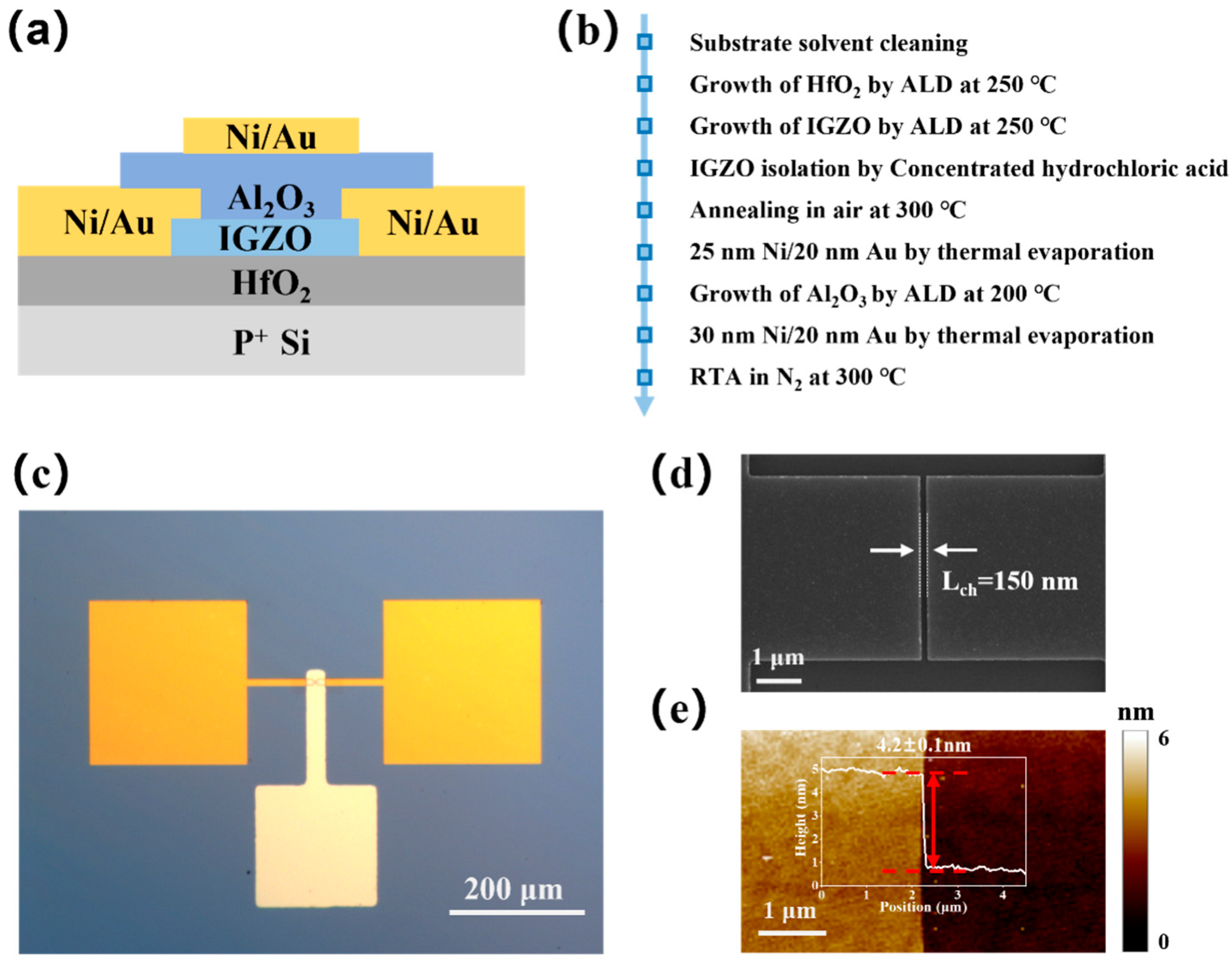
The proposed nanoscale channel length DG-TFTs were fabricated on a highly p-doped silicon wafer coated with a 9 nm thick HfO2 layer (Figure 1a). A patterned IGZO thick layer was deposited on the substrate, functioning as the carrier transport channel. A pair of Ni/Au stack electrodes, separated by a nanoscale gap, were placed on the semiconductor layer. These electrodes were fabricated using EBL and high-vacuum deposition techniques, forming a back-gate device. To construct the DG-TFTs, an Al2O3 dielectric layer and a patterned top gate were then deposited on the semiconductor. The detailed fabrication progress is illustrated in Figure 1b (see the Section 2). To clearly visualize the morphology of the DG-TFTs, an optical microscope is employed, and the result is shown in Figure 1c. An enlarged SEM micrograph of a typical device reveals the morphology of the nanoscale gap electrodes, indicating that the minimum Lch of 150 nm can be achieved using EBL. Figure 1e presents the micrograph of In0.24Ga0.58Zn0.18O imaged by AFM. Notably, the height profile extracted along the step confirms that the IGZO thickness is as thin as 4.2 ± 0.1 nm.
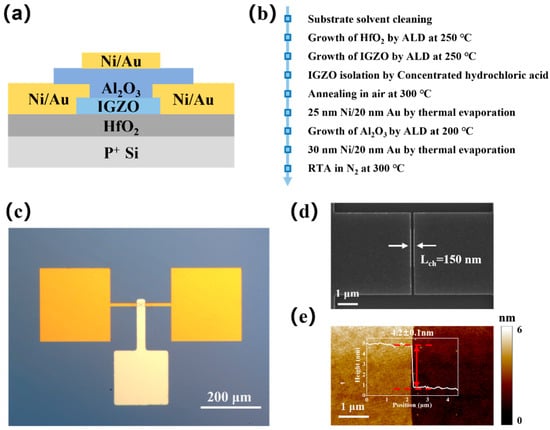
Figure 1.
Structure details and morphology characteristics of the nanoscale channel length DG-TFTs. (a) Schematic cross-sectional view of the device structure. (b) Fabrication process flow of the IGZO DG-TFTs. (c) Optical image of the device. (d) SEM micrography of a typical device’s channel. (e) Micrograph of In0.24Ga0.58Zn0.18O imaged by AFM. Insets: height profile of the patterned IGZO layer extracted from the step.
3.2. Bottom-Gate IGZO Measurements
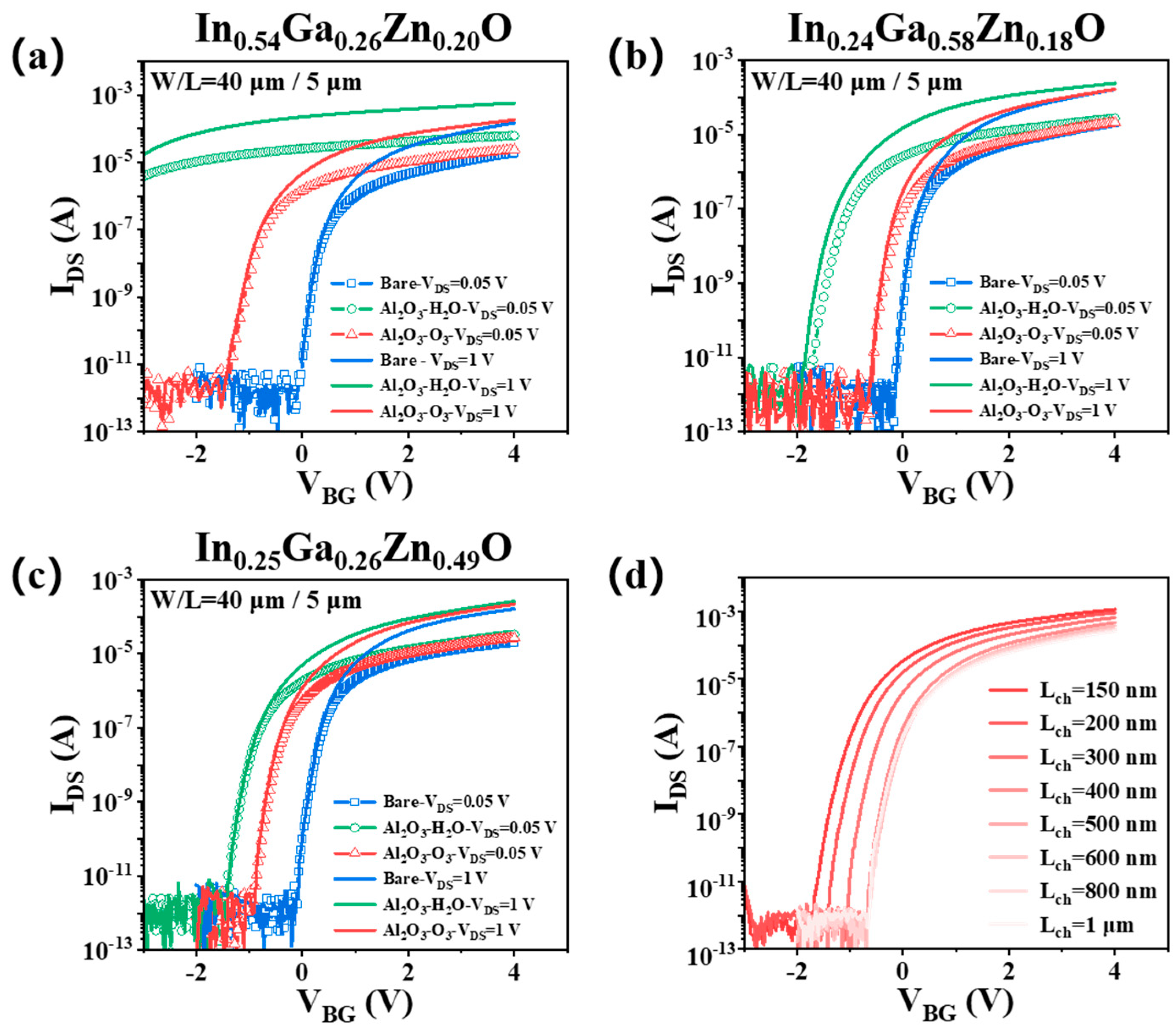
To investigate the impact of metal ratios in IGZO and the selection of precursors for the dielectric layer on device performance, a series of bottom-gate microscale TFTs with a channel width of 40 μm and Lch of 5 μm were fabricated and characterized. Figure 2a–c display the transfer characteristic curves for three different metal ratios measured by XPS of IGZO before and after capping an Al2O3 layer of 12 nm thickness, using H2O and O3 as the oxygen precursors, namely In0.54Ga0.26Zn0.20O, In0.24Ga0.58Zn0.18O, and In0.25Ga0.26Zn0.49O. The thickness of the bare channel layer is 3.2 ± 0.1 nm, 4.2 ± 0.1 nm, and 4.3 ± 0.1 nm, respectively (Figure S1). As for the bare devices, the results indicate that the electrical performances are relatively insensitive to the variations in the metal ratio. However, after covering Al2O3 using H2O as the oxygen precursor, the measured transfer characteristic curves reveal a negative shift in the VT, particularly for In0.54Ga0.26Zn0.20O, which has a higher ratio of In (depicted by green lines in Figure 2a–c). In comparison, when Al2O3 was deposited using O3 as the oxygen precursor, the transfer characteristic curves demonstrate a significant improvement in the negative shift behavior for all three distinct IGZO metal ratios (depicted by the red lines in Figure 2a–c). As shown in Figure S2, the results reveal that the devices exhibit significantly similar characteristics compared to the non-ALD processed devices after RTA at 300 °C in N2 for 5 min.
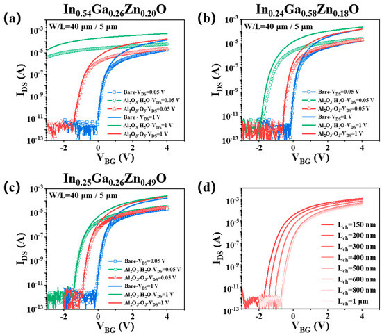
Figure 2.
Bottom-gate transfer characteristic curves for IGZO TFTs with various metal ratios before and after the deposition of Al2O3 dielectric layer. (a–c) Transfer characteristic curves for the bare semiconductor layer and those covered with Al2O3 using H2O and O3 as the oxygen precursors before RTA treatment for three distinct IGZO metal ratios: In0.54Ga0.26Zn0.20O (a), In0.24Ga0.58Zn0.18O (b), and In0.25Ga0.26Zn0.49O (c). (d) Bottom-gate transfer characteristic curves for the DG-TFTs based on In0.24Ga0.58Zn0.18O with Lch scaled down from 1 μm to 150 nm after RTA treatment. For all measurement results, the bottom-gate leakage current is less than 10−9 A.
The result of top-gate measurement for In0.24Ga0.58Zn0.18O using O3 as the oxygen precursor before and after RTA is shown in Figure S4. The SS and is 198 mv/dec and ~3.81 × 10⁻⁷ F·cm−2 before RTA and 108 mv/dec and ~4.07 × 10⁻⁷ F·cm−2 after RTA. The trap state density () at the channel and gate dielectric interface can be estimated by the SS value using the following relationship [25]:
where is the Boltzmann constant, is the absolute temperature, is the elementary electron charge, and is the capacitance per unit area of the gate dielectric. The calculated for the top-gate device is 5.53 × 10¹² eV−1cm−2 before RTA and 2.07 × 10¹² eV−1cm−2. After RTA treatment, the can be effectively decreased.
We can elucidate the physical reasons underlying the observed phenomena. First, residual hydrogen from the H2O precursor can induce hydrogen doping in the semiconductor layer. Second, the residual trimethylaluminum (TMA) precursor may strip chemisorbed oxygen or hydroxyl (-OH) groups from the oxide channel, resulting in the generation of oxygen vacancies (Vo) [26,27,28,29]. Third, during the ALD process in Al2O3 deposition, chemical reactions may occur at the interface between aluminum (Al) and IGZO, leading to the formation of numerous defects, such as metal interstitials (Mi) and Vo [27,30]. All these doping effects and defects can increase the electron density in the channel, thereby influencing the switching characteristics of the transistors. The comparison of the two precursors indicates that O3 can effectively passivate the pre-treated IGZO surface, reducing the formation of vacancies and reintroducing -OH groups into the channel, thereby suppressing the interfacial reactions that lead to defect formation (further analysis and validation can be seen in Figure 3). Notably, increasing the ratio of Ga is found to be more effective in suppressing the negative shift than increasing the ratio of In and Zn. This can be attributed to the high ionic potential of Ga3+, which allows it to form stronger bonds with oxygen ions [31]. The Ga-O bond dissociation energy is higher than that of Zn-O, enabling Ga to more effectively inhibit the formation of oxygen vacancies and reduce the concentration of free electrons in the channel. Based on the data presented in Figure 2a–c and Figure S3 and the comprehensive analysis of electrical characteristics in Table S1, we ultimately selected In0.24Ga0.58Zn0.18O with the sub-cycle of 5:2:1, O3 as the oxygen precursor in Al2O3 deposition, and RTA for the fabrication of scaled dual-gate IGZO transistors. As shown in Figure 2d, when employing the above process, the transfer characteristic curves of the device exhibit the similar VT for Lch larger than 400 nm. When scaling down Lch from 400 nm to 150 nm, the negative shift behavior and switching characteristics remain well-preserved with Ion/off > 109, indicating that the short channel effect can be effectively suppressed.
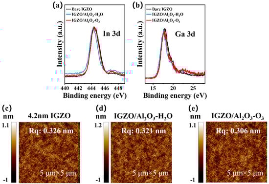
Figure 3.
Characterization of the patterned IGZO layer. (a) In 3d and (b) Ga 3d signals for the bare and 2 nm Al2O3-capped IGZO films deposited by ALD using O3 and H2O as the oxygen precursors. AFM images of (c) the IGZO film and IGZO/Al2O3 film using (d) H2O and (e) O3 as the oxygen precursors, respectively.
To further analyze and validate the influence of the precursors in the ALD process, we compared the chemical states using XPS among bare IGZO with the metal ratio of In–Ga–Zn = 0.24:0.58:0.18, IGZO covered with Al2O3 using O3 as the precursor (Al2O3 -O3), and IGZO covered with Al2O3 using H2O as the precursor (Al2O3 -H2O). As shown in Figure 3a,b, the In 3d and Ga 3d peaks of Al2O3 -O3 capped IGZO exhibit notable shifts toward lower binding energies by 0.1 eV and 0.13 eV, respectively, compared to the bare IGZO sample. In contrast, the corresponding peaks for the Al2O3-H2O capped IGZO show more pronounced shifts of 0.25 eV and 0.2 eV, respectively. These reduced binding energies are attributed to the Mi defects or Vo defects on the IGZO surface, as well as the residual reaction products that may form during the Al2O3 deposition process. These defects and reaction products can alter the local electronic environment, thereby influencing the binding energies of the In and Ga. When O3 is used as the oxygen precursor for the deposition of the Al2O3 layer, the magnitude of the peak shift is less than that using H2O. As shown in Figure S5, the Vo of Al2O3 deposited using O3 (12.57%) is less than that deposited using H2O (28.94%), which shows that the Al2O3 deposited using O3 possesses better film quality and the process can lead to less impact of the pre-treated IGZO channel layer (the O 1s spectrum for IGZO is largely influenced by the Al-O-Al peak of Al2O3 around 531.2 eV) [32]. AFM was employed to investigate the surface morphology of the IGZO thin films with and without Al2O3 capping layers, as shown in Figure 3c–e. The Rq values were measured to be 0.326 nm for the bare IGZO layer, 0.321 nm for the IGZO/Al2O3-H2O bilayer, and 0.306 nm for the IGZO/Al2O3-O3 bilayer. The similarity in surface roughness between the uncapped IGZO and the Al2O3 capped IGZO bilayers indicates that the Al2O3 capping process does not significantly degrade the interfacial roughness between Al2O3 and IGZO. Moreover, the more substantial reduction in Rq observed for the IGZO/Al2O3-O3 bilayer compared to the IGZO/Al2O3-H2O bilayer confirms the superior uniformity achieved in the ALD process when using O3 as the oxygen precursor.
We can now determine that a defect-rich and uneven channel/dielectric interface, characterized by the presence of abundant donor-like defects, trap states, or residual impurities, can introduce additional carriers. This phenomenon significantly impacts both top-gate and bottom-gate electrical characteristics. Minimizing the interfacial defects is crucial for preserving the desired transistor characteristics, particularly in downsized transistors where such defects can severely degrade performance. Based on the findings presented in Figure 2 and Figure 3, we demonstrate that optimizing the ratio of Ga and employing O3 as the precursor for Al2O3 deposition can effectively reduce interfacial defect density, enabling the realization of enhanced electrical properties.
3.3. Scaled Dual-Gate IGZO Transistors Measurements
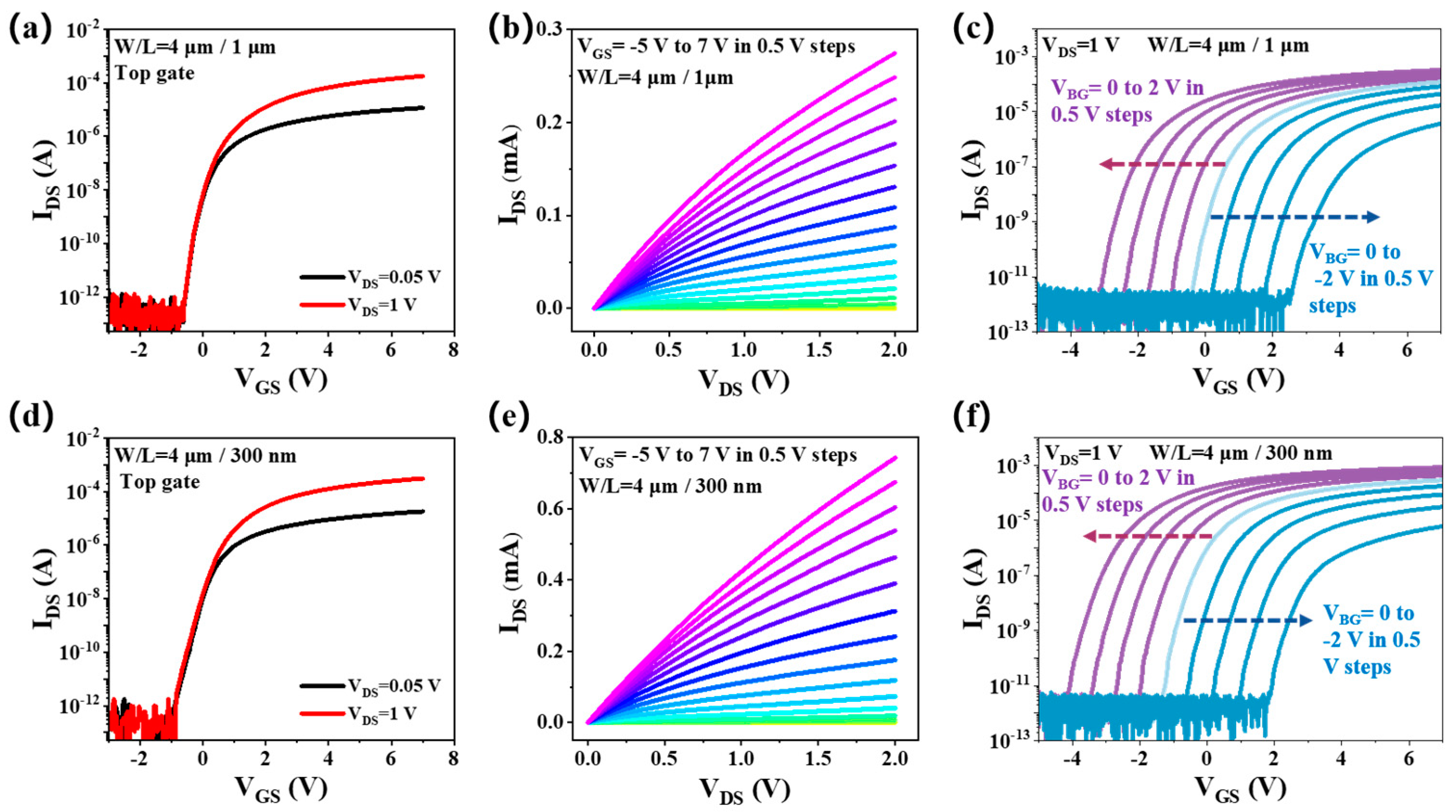
Based on the parameters derived from our previous experiments, which enabled the devices to achieve high electrical performance, we fabricated nanoscale channel length DG-TFTs with the semiconductor layer composition of In0.24Ga0.58Zn0.18O and utilized O3 as the oxygen precursor for the Al2O3 dielectric layer. Thereafter, the devices were subjected to RTA at 300 °C for 5 min in a nitrogen (N2) atmosphere, aiming to reduce the density of vacancies in the devices. Figure 4a illustrates the transfer characteristic curves controlled solely by the top gate for a device with Lch of 1 µm. By fitting the linear part of the transfer characteristic curve in linear coordinates, we measured VT values of 1.12 V and 1.05 V at drain voltages (VDS) of 0.05 V and 1 V, respectively. Detailed calculations reveal a remarkably low drain-induced barrier lowering (DIBL) of 75.68 mV/V, highlighting the excellent subthreshold characteristics of the fabricated devices, which suggests a minimal presence of defects at the IGZO/Al2O3 interface. This indicates that the fabrication process and post-treatment effectively mitigated interfacial defects. Figure 4b presents the output characteristic curves controlled only by the top gate, with gate voltage (VGS) changing from −5 V to 7 V in 0.5 V steps. The curves demonstrate that the maximum current can reach 248.2 μA at VDS = 2 V and VGS= 7 V. Moreover, the output characteristic curves show nearly linear behavior without deterioration, suggesting that our devices exhibit a weak self-heating effect. Transfer characteristics of the DG-TFTs were further examined with the VDS at 1 V and the bottom-gate voltage (VBG) varying from −2 V to 2 V in 0.5 V increments, as illustrated in Figure 4c. The results indicate that the VT shifts toward the negative direction as the VBG is gradually increased to 2 V, demonstrating that the top gate remains effective in modulating the device behavior. Conversely, when the VBG decreased from 0 V to −2 V, the VT shifts toward the positive direction. This behavior illustrates the robust dual-gate control and the ability to finely tune the device characteristics through both top- and bottom-gate voltage bias.
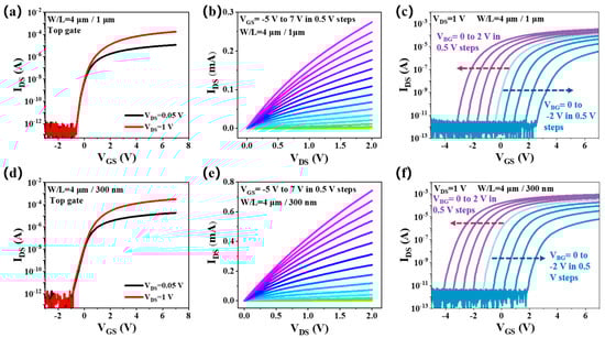
Figure 4.
Characterization of the DG-TFTs. Transfer characteristic curves of the DG-TFTs controlled by the top gate with a Lch of (a) 1 μm and (d) 300 nm. Output characteristic curves of the DG-TFTs controlled by the top gate with a Lch of (b) 1 μm and (e) 300 nm. Transfer characteristic curves (VDS = 1 V) of the DG-TFTs with a bottom-gate voltage ranging from −2 V to 2 V at 0.5 V intervals with a Lch of (c) 1 μm and (f) 300 nm.
The electrical performance of DG-TFTs was also examined when the Lch was reduced to 300 nm. The transfer characteristic curves revealed that the VT remained nearly unchanged compared to devices with Lch of 1 µm, indicating that the short channel effect was effectively mitigated through the optimized processes for IGZO layer deposition and Al2O3 precursor treatment (Figure 4a,d). Furthermore, the DIBL (78.9 mv/V) was found to be comparable to DG-TFTs with a Lch of 1 µm, suggesting minimal interface defects that could impact the transfer characteristics. The maximum drain current achieved was 742.3 µA at a VDS of 2 V, which is approximately three times higher than that observed in devices with a Lch of 1 µm (Figure 4e). The output curves also exhibit nearly linear behavior, indicating that the devices maintain a weak self-heating effect even with the reduced channel length. Figure 4f presents the transfer characteristic curves controlled by both the top gate and bottom gate. The results show that the VT shifts in the negative direction as the VBG is gradually increased to 2 V, and in the opposite direction when VBG is decreased to −2 V. This behavior is consistent with the observations in Figure 4c, demonstrating that the dual-gate modulation remains effective even with the reduced channel length. At VBG of 0 V, 0.5 V, and 1 V, the drain current is 6 pA, 27.2 nA, and 1.76 μA under VTG of −0.6 V, respectively. A high current switching ratio of 3 × 10⁵ is achieved with only 1 V modulation, demonstrating exceptional gate control efficiency with low modulated voltage.
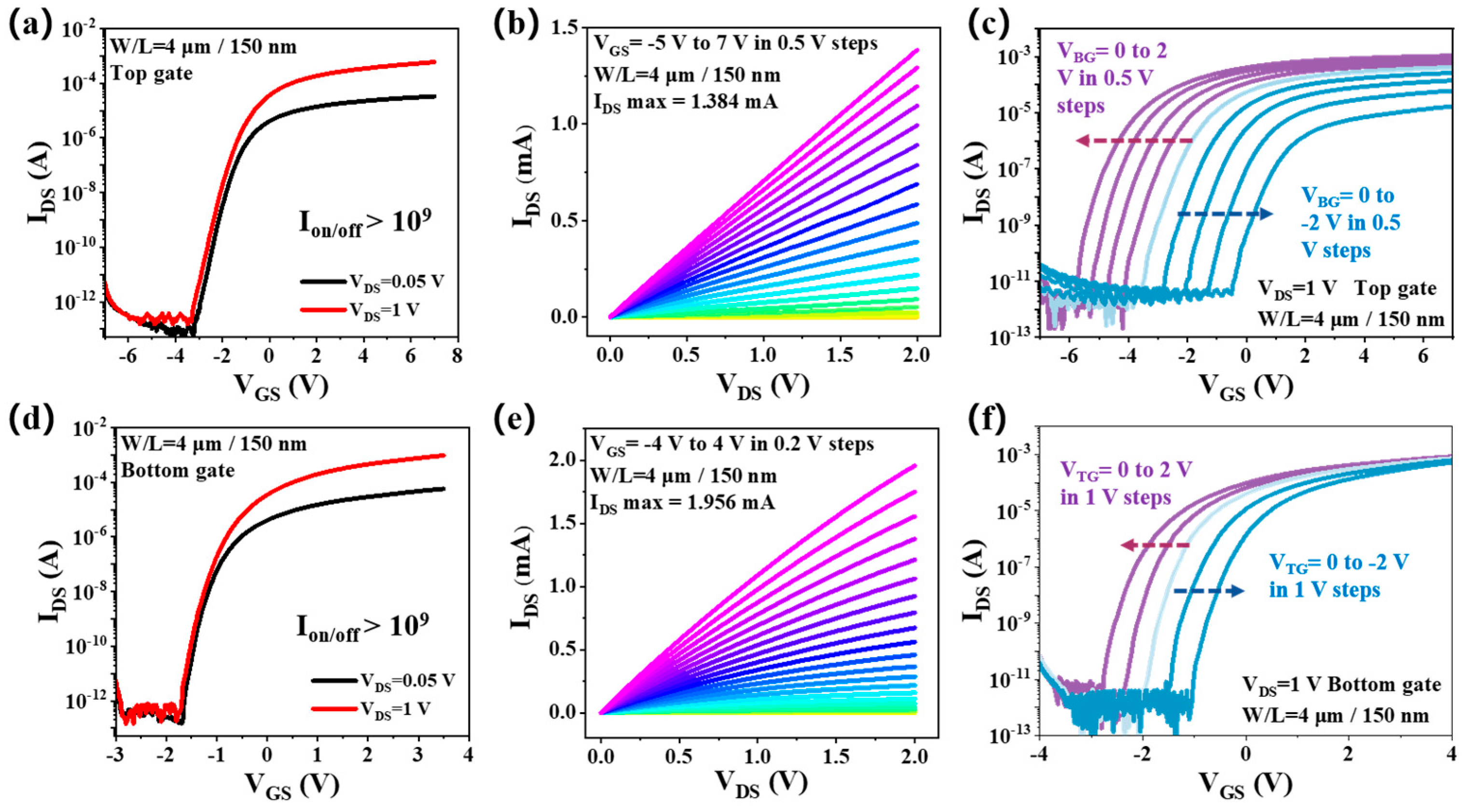
Utilizing EBL technology, the Lch of the DG-TFTs can be further scaled down to 150 nm without compromising their performance. As shown in Figure 5a, the transfer characteristic curves modulated solely by the top gate exhibit a negative shift in the VT to −0.75 V and −0.88 V at VDS of 0.05 V and 1 V, respectively. Precise calculations reveal that Ion/off exceeds 109, while the μeff is measured at 11.68 cm2V⁻1s⁻1. Compared to DG-TFTs with a Lch of 300 nm, the DIBL increases to 136.9 mV/V. This increase is attributed to the enhanced electric field between the source and drain electrodes, which can adversely affect the VT and DIBL. Figure 5b displays the output characteristic curves modulated solely by top-gate voltage, which varies from −5 to 7 V in 0.5 V increments. When the bottom-gate voltage is held constant, the device can be effectively modulated by the top gate without any noticeable performance degradation (Figure 5c). This behavior demonstrates that the dual-gate configuration can efficiently control the device performance, even with a further reduced channel length. A current switch ratio of 2 × 10⁴ can be achieved only with 1 V modulation, which can be used in high-sensitive detectors or low-power circuitry with outstanding performance. Figure 5d presents the transfer characteristic curves when the device is controlled exclusively by the bottom gate. The transfer characteristic curves in Figure 5b,e exhibit nearly linear behavior, suggesting that the device with such a short channel length also shows a weak self-heating effect despite its 150 nm channel length. For the transfer characteristic curves shown in Figure 5f, the results are obtained under dual-gate modulation with the top gate held constant. These results show that the VT shift to a negative direction under positive bias and the shift to a positive direction under negative bias are consistent with those in Figure 5c. Collectively, these findings confirm the stability and reliability of dual-gate modulation even at the hundred-nanometer scale.
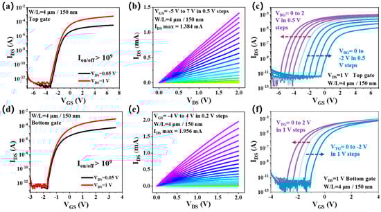
Figure 5.
Electrical performance of the DG-TFTs with their Lch scaled down to 150 nm. (a,b) Transfer and output characteristic curves of the DG-TFTs controlled only by the top gate. (c) Transfer characteristic curves modulated by the dual gate (VDS = 1 V), with the bottom-gate voltage held constant and increased from −2 to 2 V in 0.5 V intervals. (d,e) Transfer and output characteristic curves of the device controlled only by the bottom gate, respectively. (f) Transfer characteristic curves modulated by the dual gate (VDS = 1 V), with the top-gate voltage held constant and increased from −2 to 2 V in 1 V intervals.
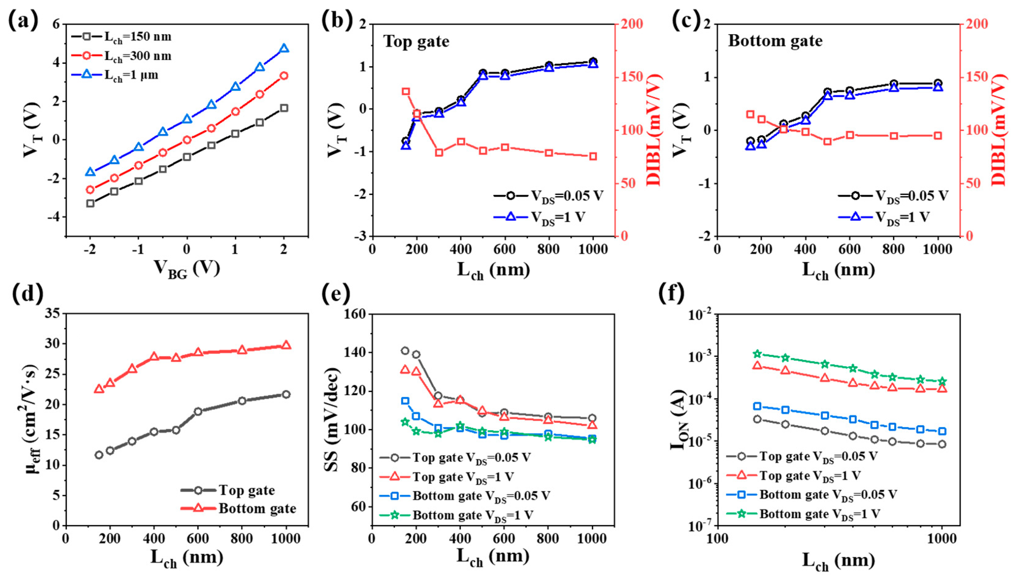
To clearly illustrate the performance of the nanoscale channel length DG-TFTs, we conducted a comprehensive summary of the modulation characteristics of the devices with channel length ranging from 1 µm to 150 nm. The data points are derived from the average of at least five individual devices, ensuring the reliability and reproducibility of the results. Figure 6a illustrates the variation in the VT of the DG-TFTs with the VBG ranging from −2 V to 2 V in 0.5 V increments. The shift in VT exhibits a linear relationship with the bottom-gate voltage for channel lengths of 150 nm, 300 nm, and 1 µm. Notably, even under low modulation voltages, the shift in VT is significant. Figure 6b,c present the VT and DIBL of the devices modulated by the top gate and bottom gate, respectively. As the channel length scales down, the VT shifts towards the negative direction due to the short channel effect. However, the DIBL remains relatively low, attributed to the high-quality, few-defect-contaminated interfaces between the semiconductor and the dielectric layers of both the top gate and bottom gate. As illustrated in Figure 6d, the effective mobility decreases from 21.54 cm2V−1s−1 to 11.68 cm2V−1s−1 for the top-gate measurement, while this value deceases from 29.7 cm2V−1s−1 to 22.46 cm2V−1s−1 for the bottom-gate measurement as the channel length is reduced. The decline in µeff can be attributed to the enhancement of interfacial scattering and the increased contact resistance when the Lch is scaled down to 150 nm [33]. The difference can be attributed to the better interface between IGZO and HfO2 (annealing at 350 °C in air for 2 h) and relatively poor interface between IGZO and Al2O3 (limited by thermal budge due to the metal electrode and worsened by TMA during the ALD process) [34]. Figure 6e shows the SS as a function of Lch under top-gate and bottom-gate modulation, respectively. Minimum SS values of 102.4 mV/dec for the top gate and 94.8 mV/dec for the bottom gate are achieved. The observed SS degradation predominantly originates from interface defects that concurrently degrade device performance [35,36,37]. These defects act as scattering centers that diminish carrier mobility while simultaneously functioning as charge-trapping sites that impede carrier transport. On-current (ION) curves show that the devices predominantly follow a 1/L scaling trend, which can be attributed to the low drain-source voltage and the suppression of the self-heating effect.
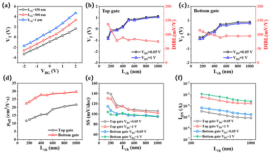
Figure 6.
Summary of the characteristics of the DG-TFTs. (a) Threshold voltage as a function of the bottom gate with three channel lengths: 150 nm, 300 nm, and 1 µm. Measured threshold voltage and DIBL as a function of Lch at two distinct bias voltages under (b) top-gate and (c) bottom-gate modulation. (d) Calculated field-effective mobility depending on channel length under top-gate and bottom-gate control, respectively. Relationships between measured (e) SS as well as (f) on-current and Lch at two distinct bias voltages under top-gate and bottom-gate control, respectively.
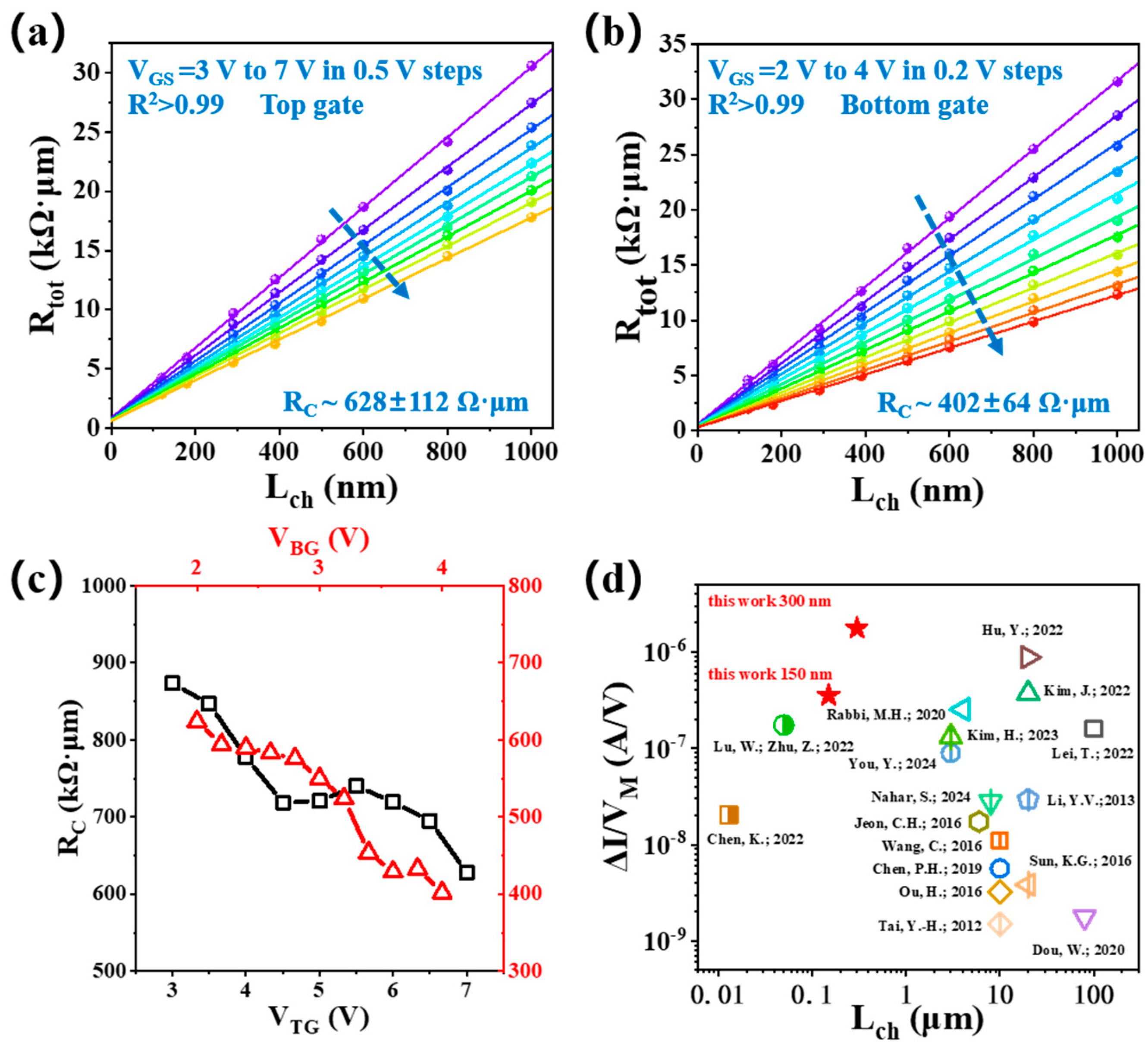
To comprehensively elucidate the electrical characteristics of the DG-TFTs after increasing the ratio of Ga, we employed the transmission-line modeling (TLM) method to calculate the contact resistance (Rc) [38]:
Here, , , and are the total resistance, threshold voltage, and contact resistance, respectively. The exhibits a linear decrease as the channel length is reduced, particularly for devices under top-gate control (Figure 7a) and bottom-gate control (Figure 7b). Figure 7b illustrates the dependence of on the top-gate voltage, as extracted from TLM measurements at VDS = 0.06 V. A low contact resistance of 628 ± 112 Ω·μm at VGS = 7 V for the top gate and 402 ± 64 Ω·μm at VGS = 4 V was obtained from the y-axis intercept for the top-gate and bottom-gate measurements, indicating effective electrical contact between the electrodes and the semiconductor. The difference in extracted from top-gate and bottom-gate measurements can contribute to the effect of transverse source-drain electric field and the quality of the interface between IGZO and the top dielectric [39]. To further highlight the superior electrical performance of our devices, we compared them with previously reported works, as shown in Figure 7c. The benchmark is defined as the normalized current divided by the modulation voltage (ΔI/VM), where ΔI represents the current change under various modulation voltages (VM). Our devices achieve a high normalized current variation exceeding 106, despite their nanoscale channel lengths. This performance underscores their suitability for the fabrication of high-performance detectors.
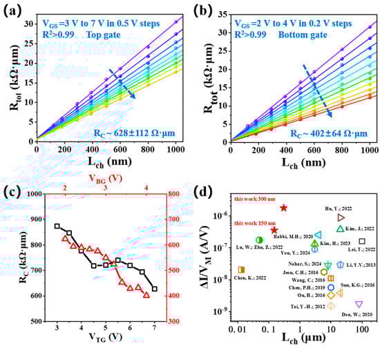
Figure 7.
Calculated contact resistance and comparison with precious works. Total resistance as a function of Lch for (a) top-gate IGZO TFTs with VGS from 3 V to 7 V in 0.5 V intervals and (b) bottom-gate IGZO TFTs with VGS from 2 V to 4 V in 0.2 V intervals. (c) Contact resistance at VDS = 0.06 V extracted from TLM. (d) The comparison of the benchmark of normalized current divided by modulation voltage with previous work [13,40,41,42,43,44,45,46,47,48,49,50,51,52,53,54,55].
4. Conclusions
In summary, we have successfully demonstrated nanoscale channel length DG-TFTs with semiconductor and dielectric layers deposited using ALD technology. By carefully optimizing the deposition parameters, we achieved a high maximum current of 1.384 mA for the top gate and 1.956 mA for the bottom gate, as well as a low contact resistance of approximately 628 Ω·μm for the top gate and 402 Ω·μm for the bottom gate. Excellent low-voltage modulation capabilities were realized through dual-gate control. Notably, high current switching ratios of 3 × 10⁵ for Lch of 300 nm and 2 × 10⁴ for Lch = 150 nm were achieved with only 1 V of gate modulation voltage. We further demonstrated that increasing the Ga ratio and using O3 as the precursor can significantly suppress the defects at the interface between the IGZO and dielectric layers. Additionally, when scaling down the Lch to 150 nm, these processes effectively mitigate short channel effects while maintaining robust device performance. These findings are crucial for the advancement of dual-gate IGZO transistor research and open up vast new opportunities for applications in high-performance detectors, BEOL integration, and 3D integration technologies.
Supplementary Materials
The following supporting information can be downloaded at: https://www.mdpi.com/article/10.3390/electronics14071257/s1, Figure S1. Height profile of the patterned IGZO layer extracted from the step for three distinct IGZO metal ratios: (a) In0.54Ga0.26Zn0.20O, (b) In0.24Ga0.58Zn0.18O, and (c) In0.25Ga0.26Zn0.49O. Figure S2. Bottom-gate transfer characteristic curves for IGZO TFTs covered with Al2O3 using H2O and O3 as the oxygen precursors before and after RTA for three distinct IGZO metal ratios: (a) In0.54Ga0.26Zn0.20O, (b) In0.24Ga0.58Zn0.18O, and (c) In0.25Ga0.26Zn0.49O. Figure S3. Bottom-gate transfer characteristic curves for the bare semiconductor layer and those covered with Al2O3 using O3 as the oxygen precursor for two distinct IGZO sub-cycle ratios: In₂O₃:Ga₂O₃:ZnO equaling (a) 5:3:1 and (b) 5:1:5. Figure S4. Top-gate transfer characteristic curves for IGZO TFTs with Al2O3 using O3 as the oxygen precursor before and after RTA for In0.24Ga0.58Zn0.18O. Figure S5. O 1s signals for (a) Bare and 2 nm Al2O3-capped IGZO films deposited by ALD using O3 as the oxygen precursor and for Al2O3 deposited by ALD using (b) O3 and (c) H2O as the oxygen precursors, respectively. Table S1. The comparison of different IGZO compositions with and without Al2O3 capping using O3 and H2O as the oxygen precursors before RTA.
Author Contributions
Conceptualization, M.W., L.Z., and C.L.; methodology, H.Z., Z.Y., and L.Z.; validation, H.Z., and L.Z.; formal analysis, H.Z., M.W., and B.L.; investigation, H.Z., Z.Y., and L.Z.; resources, C.L.; data curation, H.Z.; writing—original draft preparation, H.Z. and L.Z.; writing—review and editing, H.Z., M.W., and B.L.; visualization, H.Z. and Z.Y.; supervision, H.Z. and L.Z.; project administration, C.L.; funding acquisition, C.L. and B.L. All authors have read and agreed to the published version of the manuscript.
Funding
This work was supported in part by the National Key Research and Development Program of China (2021YFB3600701) and the National Natural Science Foundation of China under Grant U24A20297.
Data Availability Statement
Data are contained within the article.
Conflicts of Interest
The authors declare no conflicts of interest.
References
- Yoon, Y.J.; Seo, J.H.; Cho, S.; Lee, J.-H.; Kang, I.M. A polycrystalline-silicon dual-gate MOSFET-based 1T-DRAM using grain boundary-induced variable resistance. Appl. Phys. Lett. 2019, 114, 183503. [Google Scholar] [CrossRef]
- Priyadarshi, S.; Billah, M.M.; Kim, H.; Rabbi, M.H.; Urmi, S.S.; Lee, S.; Jang, J. High-performance dual gate amorphous InGaZnO thin film transistor with top gate to drain offset. IEEE Electron Device Lett. 2021, 43, 56–59. [Google Scholar] [CrossRef]
- Fuhrer, M.S.; Hone, J. Measurement of mobility in dual-gated MoS2 transistors. Nat. Nanotechnol. 2013, 8, 146–147. [Google Scholar]
- Spijkman, M.J.; Brondijk, J.J.; Geuns, T.C.; Smits, E.C.; Cramer, T.; Zerbetto, F.; Stoliar, P.; Biscarini, F.; Blom, P.W.; de Leeuw, D.M. Dual-gate organic field-effect transistors as potentiometric sensors in aqueous solution. Adv. Funct. Mater. 2010, 20, 898–905. [Google Scholar]
- Sheng, J.; Lee, H.-J.; Oh, S.; Park, J.-S. Flexible and High-Performance Amorphous Indium Zinc Oxide Thin-Film Transistor Using Low-Temperature Atomic Layer Deposition. ACS Appl. Mater. Interfaces 2016, 8, 33821–33828. [Google Scholar]
- Kamiya, T.; Hosono, H. Material characteristics and applications of transparent amorphous oxide semiconductors. NPG Asia Mater. 2010, 2, 15–22. [Google Scholar]
- Kamiya, T.; Nomura, K.; Hosono, H. Present status of amorphous In–Ga–Zn–O thin-film transistors. Sci. Technol. Adv. Mater. 2010, 11, 044305. [Google Scholar]
- Hong, T.; Jeong, H.-J.; Lee, H.-M.; Choi, S.-H.; Lim, J.H.; Park, J.-S. Significance of pairing In/Ga precursor structures on PEALD InGaOx thin-film transistor. ACS Appl. Mater. Interfaces 2021, 13, 28493–28502. [Google Scholar]
- Ji, D.; Jang, J.; Park, J.H.; Kim, D.; Rim, Y.S.; Hwang, D.K.; Noh, Y.-Y. Recent progress in the development of backplane thin film transistors for information displays. J. Inf. Disp. 2021, 22, 1–11. [Google Scholar] [CrossRef]
- Zou, T.; Chen, C.; Xiang, B.; Wang, Y.; Liu, C.; Zhang, S.; Zhou, H. Flexible, active-matrix flat-panel image sensor for low dose X-ray detection enabled by integration of perovskite photodiode and oxide thin film transistor. In Proceedings of the 2019 IEEE International Electron Devices Meeting (IEDM), San Francisco, CA, USA, 7–11 December 2019; pp. 8.5.1–8.5.4. [Google Scholar]
- Lee, S.; Nathan, A. Subthreshold Schottky-barrier thin-film transistors with ultralow power and high intrinsic gain. Science 2016, 354, 302–304. [Google Scholar]
- Belmonte, A.; Oh, H.; Rassoul, N.; Donadio, G.; Mitard, J.; Dekkers, H.; Delhougne, R.; Subhechha, S.; Chasin, A.; Van Setten, M.; et al. Capacitor-less, long-retention (>400s) DRAM cell paving the way towards low-power and high-density monolithic 3D DRAM. In Proceedings of the 2020 IEEE International Electron Devices Meeting (IEDM), San Francisco, CA, USA, 12–18 December 2020; pp. 28.22.21–28.22.24. [Google Scholar]
- Kim, J.; Jeong, S.; Sarawut, S.; Kim, H.; Son, S.U.; Lee, S.; Rabbani, G.; Kwon, H.; Lim, E.-K.; Ahn, S.N.; et al. An immunosensor based on a high performance dual-gate oxide semiconductor thin-film transistor for rapid detection of SARS-CoV-2. Lab a Chip 2022, 22, 899–907. [Google Scholar] [CrossRef]
- Xiang, B.; Zou, T.; Wang, Y.; Liu, C.; Chen, J.; Wang, K.; Dai, Q.; Zhang, S.; Zhou, H. Photovoltage-coupled dual-gate InGaZnO thin-film transistors operated at the subthreshold region for low-power photodetection. ACS Appl. Electron. Mater. 2020, 2, 1745–1751. [Google Scholar] [CrossRef]
- Ma, P.; Sun, J.; Liang, G.; Li, Y.; Xin, Q.; Li, Y.; Song, A. Half-volt operation of IGZO thin-film transistors enabled by ultrathin HfO2 gate dielectric. Appl. Phys. Lett. 2018, 113, 063501. [Google Scholar] [CrossRef]
- Samanta, S.; Chand, U.; Xu, S.; Han, K.; Wu, Y.; Wang, C.; Kumar, A.; Velluri, H.; Li, Y.; Fong, X.; et al. Low subthreshold swing and high mobility amorphous indium–gallium–zinc-oxide thin-film transistor with thin HfO2 gate dielectric and excellent uniformity. IEEE Electron Device Lett. 2020, 41, 856–859. [Google Scholar] [CrossRef]
- Ma, P.; Du, L.; Wang, Y.; Jiang, R.; Xin, Q.; Li, Y.; Song, A. Low voltage operation of IGZO thin film transistors enabled by ultrathin Al2O3 gate dielectric. Appl. Phys. Lett. 2018, 112, 023501. [Google Scholar] [CrossRef]
- Shao, Y.; Xiao, X.; He, X.; Deng, W.; Zhang, S. Low-voltage a-InGaZnO thin-film transistors with anodized thin HfO2 gate dielectric. IEEE Electron Device Lett. 2015, 36, 573–575. [Google Scholar] [CrossRef]
- Lee, S.Y.; Kim, J.; Park, A.; Park, J.; Seo, H. Creation of a short-range ordered two-dimensional electron gas channel in Al2O3/In2O3 interfaces. ACS Nano 2017, 11, 6040–6047. [Google Scholar] [CrossRef]
- Park, J.; Kim, H.; Choi, P.; Jeon, B.; Lee, J.; Oh, C.; Kim, B.; Choi, B. Effect of ALD-and PEALD-grown Al2O3 gate insulators on electrical and stability properties for a-IGZO thin-film transistor. Electron. Mater. Lett. 2021, 17, 299–306. [Google Scholar] [CrossRef]
- Seok, T.J.; Liu, Y.; Jung, H.J.; Kim, S.B.; Kim, D.H.; Kim, S.M.; Jang, J.H.; Cho, D.-Y.; Lee, S.W.; Park, T.J. Field-effect device using quasi-two-dimensional electron gas in mass-producible atomic-layer-deposited Al2O3/TiO2 ultrathin (<10 nm) film heterostructures. ACS Nano 2018, 12, 10403–10409. [Google Scholar]
- Jeon, S.; Park, S.; Song, I.; Hur, J.-H.; Park, J.; Kim, S.; Kim, S.; Yin, H.; Lee, E.; Ahn, S.; et al. 180nm gate length amorphous InGaZnO thin film transistor for high density image sensor applications. In Proceedings of the 2010 International Electron Devices Meeting, San Francisco, CA, USA, 6–8 December 2010; pp. 21.23.21–21.23.24. [Google Scholar]
- Kang, I.H.; Hwang, S.H.; Baek, Y.J.; Kim, S.G.; Han, Y.L.; Kang, M.S.; Woo, J.G.; Lee, J.M.; Yu, E.S.; Bae, B.S. Interfacial oxidized gate insulators for low-power oxide thin-film transistors. ACS Omega 2021, 6, 2717–2726. [Google Scholar] [CrossRef]
- Han, K.; Samanta, S.; Sun, C.; Gong, X. Top-gate short channel amorphous indium-gallium-zinc-oxide thin film transistors with sub-1.2 nm equivalent oxide thickness. IEEE J. Electron Devices Soc. 2021, 9, 1125–1130. [Google Scholar] [CrossRef]
- Zhu, L.; He, Y.; Chen, C.; Wang, X.; Zhu, Y.; Zhu, Y.; Mao, H.; Wan, C.; Wan, Q. High-Performance Amorphous InGaZnO Thin-Film Transistor Gated by HfAlOx Dielectric With Ultralow Subthreshold Swing. IEEE Trans. Electron Devices 2021, 68, 6154–6158. [Google Scholar]
- Han, K.; Kong, Q.; Kang, Y.; Sun, C.; Wang, C.; Zhang, J.; Xu, H.; Samanta, S.; Zhou, J.; Wang, H. Indium-gallium-zinc-oxide (IGZO) nanowire transistors. IEEE Trans. Electron Devices 2021, 68, 6610–6616. [Google Scholar]
- Yang, H.; Zhou, X.; Fu, H.; Chang, B.; Min, Y.; Peng, H.; Lu, L.; Zhang, S. Metal reaction-induced bulk-doping effect in forming conductive source-drain regions of self-aligned top-gate amorphous InGaZnO thin-film transistors. ACS Appl. Mater. Interfaces 2021, 13, 11442–11448. [Google Scholar]
- Allemang, C.R.; Peterson, R.L. Passivation of thin channel zinc tin oxide TFTs using Al2O3 deposited by O3-based atomic layer deposition. IEEE Electron Device Lett. 2019, 40, 1120–1123. [Google Scholar]
- Zywotko, D.R.; George, S.M. Thermal atomic layer etching of ZnO by a “Conversion-Etch” mechanism using sequential exposures of hydrogen fluoride and trimethylaluminum. Chem. Mater. 2017, 29, 1183–1191. [Google Scholar]
- Li, J.; Zhang, Y.; Wang, J.; Yang, H.; Zhou, X.; Chan, M.; Wang, X.; Lu, L.; Zhang, S. Near-ideal top-gate controllability of InGaZnO thin-film transistors by suppressing interface defects with an ultrathin atomic layer deposited gate insulator. ACS Appl. Mater. Interfaces 2023, 15, 8666–8675. [Google Scholar]
- Kim, H.Y.; Jung, E.A.; Mun, G.; Agbenyeke, R.E.; Park, B.K.; Park, J.-S.; Son, S.U.; Jeon, D.J.; Park, S.-H.K.; Chung, T.-M.; et al. Low-temperature growth of indium oxide thin film by plasma-enhanced atomic layer deposition using liquid dimethyl (N-ethoxy-2, 2-dimethylpropanamido) indium for high-mobility thin film transistor application. ACS Appl. Mater. Interfaces 2016, 8, 26924–26931. [Google Scholar]
- Haeberle, J.; Henkel, K.; Gargouri, H.; Naumann, F.; Gruska, B.; Arens, M.; Tallarida, M.; Schmeißer, D. Ellipsometry and XPS comparative studies of thermal and plasma enhanced atomic layer deposited Al2O3-films. Beilstein J. Nanotechnol. 2013, 4, 732–742. [Google Scholar]
- Valletta, A.; Fortunato, G.; Mariucci, L.; Barquinha, P.; Martins, R.; Fortunato, E.J. Contact effects in amorphous InGaZnO thin film transistors. J. Disp. Technol. 2014, 10, 956–961. [Google Scholar]
- Zheng, S.; Lv, S.; Wang, C.; Li, Z.; Dong, L.; Xin, Q.; Song, A.; Zhang, J.; Li, Y. Post-annealing effect of low temperature atomic layer deposited Al2O3 on the top gate IGZO TFT. Nanotechnology 2024, 35, 155203. [Google Scholar] [CrossRef] [PubMed]
- Charnas, A.; Si, M.; Lin, Z.; Ye, P.D. Enhancement-mode atomic-layer thin In2O3 transistors with maximum current exceeding 2 A/mm at drain voltage of 0.7 V enabled by oxygen plasma treatment. Appl. Phys. Lett. 2021, 118, 052107. [Google Scholar]
- Si, M.; Charnas, A.; Lin, Z.; Peide, D.Y. Enhancement-mode atomic-layer-deposited In2O3 transistors with maximum drain current of 2.2 A/mm at drain voltage of 0.7 V by low-temperature annealing and stability in hydrogen environment. IEEE Trans. Electron Devices 2021, 68, 1075–1080. [Google Scholar] [CrossRef]
- Si, M.; Lin, Z.; Charnas, A.; Peide, D.Y. Scaled atomic-layer-deposited indium oxide nanometer transistors with maximum drain current exceeding 2 A/mm at drain voltage of 0.7 V. IEEE Electron Device Lett. 2020, 42, 184–187. [Google Scholar]
- Guo, M.; Ou, H.; Xie, D.; Zhu, Q.; Wang, M.; Liang, L.; Liu, F.; Ning, C.; Cao, H.; Yuan, G. Critical assessment of the high carrier mobility of bilayer In2O3/IGZO transistors and the underlying mechanisms. Adv. Electron. Mater. 2023, 9, 2201184. [Google Scholar]
- Richards, T.; Sirringhaus, H. Analysis of the contact resistance in staggered, top-gate organic field-effect transistors. J. Appl. Phys. 2007, 102, 094510. [Google Scholar]
- Tai, Y.-H.; Chiu, H.-L.; Chou, L.-S.; Chang, C.-H. Boosted gain of the differential amplifier using the second gate of the dual-gate a-IGZO TFTs. IEEE Electron Device Lett. 2012, 33, 1729–1731. [Google Scholar]
- Lei, T.; Shi, R.; Wang, Y.; Xia, Z.; Wong, M. A comparative study on inverters built with dual-gate thin-film transistors based on depletion-or enhancement-mode technologies. IEEE Trans. Electron Devices 2022, 69, 3186–3191. [Google Scholar]
- You, Y.; Moon, K.C.; Kim, H.; Oh, J.; Lee, S.; Lim, J.H.; Son, K.S.; Cho, J.; Park, K. Double-gate metal–oxide TFT pixel circuit for improved luminance uniformity of mobile OLED display. J. Inf. Disp. 2024, 1–9. [Google Scholar] [CrossRef]
- Chen, P.H.; Tsao, Y.C.; Chien, Y.C.; Chiang, H.C.; Chen, H.M.; Lu, Y.H.; Shih, C.C.; Tai, M.C.; Chen, G.F.; Tsai, Y.L. A Dual-Gate InGaZnO4-Based Thin-Film Transistor for High-Sensitivity UV Detection. Adv. Mater. Technol. 2019, 4, 1900106. [Google Scholar] [CrossRef]
- Dou, W.; Tan, Y. Dual-gate low-voltage transparent electric-double-layer thin-film transistors with a top gate for threshold voltage modulation. RSC Adv. 2020, 10, 8093–8096. [Google Scholar] [CrossRef]
- Ou, H.; Wang, K.; Chen, J.; Nathan, A.; Deng, S.; Xu, N. Dual-gate photosensitive FIN-TFT with high photoconductive gain and near-UV to near-IR responsivity. In Proceedings of the 2016 IEEE International Electron Devices Meeting (IEDM), San Francisco, CA, USA, 3–7 December 2016; pp. 32.35.31–32.35.34. [Google Scholar]
- Rabbi, M.H.; Billah, M.M.; Siddik, A.B.; Lee, S.; Lee, J.; Jang, J. Extremely stable dual gate coplanar amorphous InGaZnO thin film transistor with split active layer by N2O annealing. IEEE Electron Device Lett. 2020, 41, 1782–1785. [Google Scholar] [CrossRef]
- Jeon, C.H.; Um, J.G.; Mativenga, M.; Jang, J. Fast threshold voltage compensation AMOLED pixel circuit using secondary gate effect of dual gate a-IGZO TFTs. IEEE Electron Device Lett. 2016, 37, 1450–1453. [Google Scholar] [CrossRef]
- Sun, K.G.; Choi, K.; Jackson, T.N. Low-power double-gate ZnO TFT active rectifier. IEEE Electron Device Lett. 2016, 37, 426–428. [Google Scholar] [CrossRef]
- Li, Y.V.; Ramirez, J.I.; Sun, K.G.; Jackson, T.N. Low-voltage double-gate ZnO thin-film transistor circuits. IEEE Electron Device Lett. 2013, 34, 891–893. [Google Scholar] [CrossRef]
- Hu, Y.; Wang, Y.; Lei, T.; Wang, F.; Wong, M. Neuromorphic implementation of logic functions based on parallel dual-gate thin-film transistors. IEEE Electron Device Lett. 2022, 43, 741–744. [Google Scholar] [CrossRef]
- Wang, C.; Hu, Z.; He, X.; Liao, C.; Zhang, S. One gate diode-connected dual-gate a-IGZO TFT driven pixel circuit for active matrix organic light-emitting diode displays. IEEE Trans. Electron Devices 2016, 63, 3800–3803. [Google Scholar] [CrossRef]
- Kim, H.; Kim, Y.; Lee, H. P-25: An AMOLED Pixel Circuit Compensating for Variation of Sub-threshold Swing and Threshold Voltage Based on Double Gate a-IGZO TFTs. In SID Symposium Digest of Technical Papers; Society for Information Display: Santa Ana, CA, USA, 2023; pp. 1502–1505. [Google Scholar]
- Nahar, S.; Priyadarshi, S.; Billah, M.M.; Arnob, M.R.M.; Rahaman, A.; Kim, J.B.; Bae, Y.H.; Ma, C.; Lin, Y.; Chen, B. A Study on High Performance, Dual-Gate a-IZO/a-IGZTO TFTs with Excellent Stability. IEEE Electron Device Lett. 2024, 45, 1835–1838. [Google Scholar] [CrossRef]
- Lu, W.; Zhu, Z.; Chen, K.; Liu, M.; Kang, B.-M.; Duan, X.; Niu, J.; Liao, F.; Dan, W.; Wu, X.-S. First demonstration of dual-gate IGZO 2T0C DRAM with novel read operation, one bit line in single cell, ION = 1500 μa/μm@ VDS = 1V and retention time> 300s. In Proceedings of the 2022 International Electron Devices Meeting (IEDM), San Francisco, CA, USA, 3–7 December 2022; pp. 26.24.21–26.24.24. [Google Scholar]
- Chen, K.; Niu, J.; Yang, G.; Liu, M.; Lu, W.; Liao, F.; Huang, K.; Duan, X.; Lu, C.; Wang, J. Scaling Dual-Gate Ultra-thin a-IGZO FET to 30 nm Channel Length with Record-high Gm,max of 559 µS/µm at VDS = 1 V, Record-low DIBL of 10 mV/V and Nearly Ideal SS of 63 mV/dec. In Proceedings of the 2022 IEEE Symposium on VLSI Technology and Circuits (VLSI Technology and Circuits), Honolulu, HI, USA, 12–17 June 2022; pp. 298–299. [Google Scholar]

Disclaimer/Publisher’s Note: The statements, opinions and data contained in all publications are solely those of the individual author(s) and contributor(s) and not of MDPI and/or the editor(s). MDPI and/or the editor(s) disclaim responsibility for any injury to people or property resulting from any ideas, methods, instructions or products referred to in the content. |
© 2025 by the authors. Licensee MDPI, Basel, Switzerland. This article is an open access article distributed under the terms and conditions of the Creative Commons Attribution (CC BY) license (https://creativecommons.org/licenses/by/4.0/).